EP0759609A2 - Appareil de disque optique, son circuit de commande de suivi de piste et procédé de changement de position de suivi de piste - Google Patents
Appareil de disque optique, son circuit de commande de suivi de piste et procédé de changement de position de suivi de piste Download PDFInfo
- Publication number
- EP0759609A2 EP0759609A2 EP96112901A EP96112901A EP0759609A2 EP 0759609 A2 EP0759609 A2 EP 0759609A2 EP 96112901 A EP96112901 A EP 96112901A EP 96112901 A EP96112901 A EP 96112901A EP 0759609 A2 EP0759609 A2 EP 0759609A2
- Authority
- EP
- European Patent Office
- Prior art keywords
- land
- groove
- tracking
- optical disk
- condensing
- Prior art date
- Legal status (The legal status is an assumption and is not a legal conclusion. Google has not performed a legal analysis and makes no representation as to the accuracy of the status listed.)
- Granted
Links
- 230000003287 optical effect Effects 0.000 title claims abstract description 254
- 238000000034 method Methods 0.000 title claims description 17
- 238000001514 detection method Methods 0.000 claims description 75
- 230000002401 inhibitory effect Effects 0.000 claims description 20
- 239000011521 glass Substances 0.000 description 28
- 239000000758 substrate Substances 0.000 description 24
- 238000005520 cutting process Methods 0.000 description 15
- 229920002120 photoresistant polymer Polymers 0.000 description 7
- PXHVJJICTQNCMI-UHFFFAOYSA-N Nickel Chemical compound [Ni] PXHVJJICTQNCMI-UHFFFAOYSA-N 0.000 description 6
- 238000002844 melting Methods 0.000 description 6
- 230000008018 melting Effects 0.000 description 6
- 230000002093 peripheral effect Effects 0.000 description 6
- 238000010586 diagram Methods 0.000 description 5
- 238000009713 electroplating Methods 0.000 description 3
- 238000001746 injection moulding Methods 0.000 description 3
- 229910052759 nickel Inorganic materials 0.000 description 3
- 239000004065 semiconductor Substances 0.000 description 3
- 230000009466 transformation Effects 0.000 description 3
- IXMPXTJYLZVFBW-UHFFFAOYSA-N argon neon Chemical compound [Ne].[Ne].[Ar] IXMPXTJYLZVFBW-UHFFFAOYSA-N 0.000 description 2
- 238000006243 chemical reaction Methods 0.000 description 1
- 125000004122 cyclic group Chemical group 0.000 description 1
Images





Classifications
-
- G—PHYSICS
- G11—INFORMATION STORAGE
- G11B—INFORMATION STORAGE BASED ON RELATIVE MOVEMENT BETWEEN RECORD CARRIER AND TRANSDUCER
- G11B7/00—Recording or reproducing by optical means, e.g. recording using a thermal beam of optical radiation by modifying optical properties or the physical structure, reproducing using an optical beam at lower power by sensing optical properties; Record carriers therefor
- G11B7/08—Disposition or mounting of heads or light sources relatively to record carriers
-
- G—PHYSICS
- G11—INFORMATION STORAGE
- G11B—INFORMATION STORAGE BASED ON RELATIVE MOVEMENT BETWEEN RECORD CARRIER AND TRANSDUCER
- G11B20/00—Signal processing not specific to the method of recording or reproducing; Circuits therefor
- G11B20/10—Digital recording or reproducing
- G11B20/12—Formatting, e.g. arrangement of data block or words on the record carriers
- G11B20/1217—Formatting, e.g. arrangement of data block or words on the record carriers on discs
-
- G—PHYSICS
- G11—INFORMATION STORAGE
- G11B—INFORMATION STORAGE BASED ON RELATIVE MOVEMENT BETWEEN RECORD CARRIER AND TRANSDUCER
- G11B27/00—Editing; Indexing; Addressing; Timing or synchronising; Monitoring; Measuring tape travel
- G11B27/10—Indexing; Addressing; Timing or synchronising; Measuring tape travel
- G11B27/19—Indexing; Addressing; Timing or synchronising; Measuring tape travel by using information detectable on the record carrier
-
- G—PHYSICS
- G11—INFORMATION STORAGE
- G11B—INFORMATION STORAGE BASED ON RELATIVE MOVEMENT BETWEEN RECORD CARRIER AND TRANSDUCER
- G11B27/00—Editing; Indexing; Addressing; Timing or synchronising; Monitoring; Measuring tape travel
- G11B27/10—Indexing; Addressing; Timing or synchronising; Measuring tape travel
- G11B27/19—Indexing; Addressing; Timing or synchronising; Measuring tape travel by using information detectable on the record carrier
- G11B27/28—Indexing; Addressing; Timing or synchronising; Measuring tape travel by using information detectable on the record carrier by using information signals recorded by the same method as the main recording
- G11B27/30—Indexing; Addressing; Timing or synchronising; Measuring tape travel by using information detectable on the record carrier by using information signals recorded by the same method as the main recording on the same track as the main recording
- G11B27/3027—Indexing; Addressing; Timing or synchronising; Measuring tape travel by using information detectable on the record carrier by using information signals recorded by the same method as the main recording on the same track as the main recording used signal is digitally coded
-
- G—PHYSICS
- G11—INFORMATION STORAGE
- G11B—INFORMATION STORAGE BASED ON RELATIVE MOVEMENT BETWEEN RECORD CARRIER AND TRANSDUCER
- G11B7/00—Recording or reproducing by optical means, e.g. recording using a thermal beam of optical radiation by modifying optical properties or the physical structure, reproducing using an optical beam at lower power by sensing optical properties; Record carriers therefor
- G11B7/007—Arrangement of the information on the record carrier, e.g. form of tracks, actual track shape, e.g. wobbled, or cross-section, e.g. v-shaped; Sequential information structures, e.g. sectoring or header formats within a track
- G11B7/00718—Groove and land recording, i.e. user data recorded both in the grooves and on the lands
-
- G—PHYSICS
- G11—INFORMATION STORAGE
- G11B—INFORMATION STORAGE BASED ON RELATIVE MOVEMENT BETWEEN RECORD CARRIER AND TRANSDUCER
- G11B7/00—Recording or reproducing by optical means, e.g. recording using a thermal beam of optical radiation by modifying optical properties or the physical structure, reproducing using an optical beam at lower power by sensing optical properties; Record carriers therefor
- G11B7/08—Disposition or mounting of heads or light sources relatively to record carriers
- G11B7/085—Disposition or mounting of heads or light sources relatively to record carriers with provision for moving the light beam into, or out of, its operative position or across tracks, otherwise than during the transducing operation, e.g. for adjustment or preliminary positioning or track change or selection
- G11B7/08505—Methods for track change, selection or preliminary positioning by moving the head
- G11B7/08517—Methods for track change, selection or preliminary positioning by moving the head with tracking pull-in only
-
- G—PHYSICS
- G11—INFORMATION STORAGE
- G11B—INFORMATION STORAGE BASED ON RELATIVE MOVEMENT BETWEEN RECORD CARRIER AND TRANSDUCER
- G11B2220/00—Record carriers by type
- G11B2220/20—Disc-shaped record carriers
- G11B2220/21—Disc-shaped record carriers characterised in that the disc is of read-only, rewritable, or recordable type
- G11B2220/213—Read-only discs
-
- G—PHYSICS
- G11—INFORMATION STORAGE
- G11B—INFORMATION STORAGE BASED ON RELATIVE MOVEMENT BETWEEN RECORD CARRIER AND TRANSDUCER
- G11B2220/00—Record carriers by type
- G11B2220/20—Disc-shaped record carriers
- G11B2220/25—Disc-shaped record carriers characterised in that the disc is based on a specific recording technology
- G11B2220/2537—Optical discs
- G11B2220/2545—CDs
-
- G—PHYSICS
- G11—INFORMATION STORAGE
- G11B—INFORMATION STORAGE BASED ON RELATIVE MOVEMENT BETWEEN RECORD CARRIER AND TRANSDUCER
- G11B7/00—Recording or reproducing by optical means, e.g. recording using a thermal beam of optical radiation by modifying optical properties or the physical structure, reproducing using an optical beam at lower power by sensing optical properties; Record carriers therefor
- G11B7/007—Arrangement of the information on the record carrier, e.g. form of tracks, actual track shape, e.g. wobbled, or cross-section, e.g. v-shaped; Sequential information structures, e.g. sectoring or header formats within a track
- G11B7/00745—Sectoring or header formats within a track
-
- G—PHYSICS
- G11—INFORMATION STORAGE
- G11B—INFORMATION STORAGE BASED ON RELATIVE MOVEMENT BETWEEN RECORD CARRIER AND TRANSDUCER
- G11B7/00—Recording or reproducing by optical means, e.g. recording using a thermal beam of optical radiation by modifying optical properties or the physical structure, reproducing using an optical beam at lower power by sensing optical properties; Record carriers therefor
- G11B7/007—Arrangement of the information on the record carrier, e.g. form of tracks, actual track shape, e.g. wobbled, or cross-section, e.g. v-shaped; Sequential information structures, e.g. sectoring or header formats within a track
- G11B7/013—Arrangement of the information on the record carrier, e.g. form of tracks, actual track shape, e.g. wobbled, or cross-section, e.g. v-shaped; Sequential information structures, e.g. sectoring or header formats within a track for discrete information, i.e. where each information unit is stored in a distinct discrete location, e.g. digital information formats within a data block or sector
-
- G—PHYSICS
- G11—INFORMATION STORAGE
- G11B—INFORMATION STORAGE BASED ON RELATIVE MOVEMENT BETWEEN RECORD CARRIER AND TRANSDUCER
- G11B7/00—Recording or reproducing by optical means, e.g. recording using a thermal beam of optical radiation by modifying optical properties or the physical structure, reproducing using an optical beam at lower power by sensing optical properties; Record carriers therefor
- G11B7/08—Disposition or mounting of heads or light sources relatively to record carriers
- G11B7/09—Disposition or mounting of heads or light sources relatively to record carriers with provision for moving the light beam or focus plane for the purpose of maintaining alignment of the light beam relative to the record carrier during transducing operation, e.g. to compensate for surface irregularities of the latter or for track following
- G11B7/0945—Methods for initialising servos, start-up sequences
-
- G—PHYSICS
- G11—INFORMATION STORAGE
- G11B—INFORMATION STORAGE BASED ON RELATIVE MOVEMENT BETWEEN RECORD CARRIER AND TRANSDUCER
- G11B7/00—Recording or reproducing by optical means, e.g. recording using a thermal beam of optical radiation by modifying optical properties or the physical structure, reproducing using an optical beam at lower power by sensing optical properties; Record carriers therefor
- G11B7/24—Record carriers characterised by shape, structure or physical properties, or by the selection of the material
- G11B7/26—Apparatus or processes specially adapted for the manufacture of record carriers
- G11B7/261—Preparing a master, e.g. exposing photoresist, electroforming
Definitions
- the present invention relates to an optical disk apparatus for recording data in/on both a concentrical or spiral groove and a land as the recording tracks of an optical disk, and reproducing the recorded data, a tracking control circuit therefor, and a method of changing a tracking position.
- optical disks include an optical disk on which data is recorded in only a guide groove (groove) or from which the data in the groove is reproduced, and an optical disk (CD-ROM) on which data is recorded by forming record marks representing data in a virtual guide groove in advance in an optical disk mastering process. Tracking is performed for such an optical disk by using a track error signal (tracking detection output) obtained from a guide groove (groove) or a record mark. In this operation, the tracking polarity is set to one direction (positive phase), and data is recorded or reproduced.
- track error signal tilt detection output
- the polarity of a track error signal (the polarity of a tracking detection output) used to perform tracking must be inverted in accordance with tracking for guide grooves (grooves) or tracking for flat portions (lands).
- the polarity of the tracking detection output is set to a positive phase.
- the polarity of the tracking detection output is set to an opposite or negative phase.
- the tracking position is changed from a groove to a land by simply switching the polarity of the tracking detection output from the positive phase to the opposite phase, whereas the tracking position is changed from the land to the groove by switching the opposite phase to the positive phase.
- the tracking position cannot therefore be accurately changed from the groove or land to the land or groove.
- conventional optical disks do not include an optical disk in which lands and grooves are alternately present in units of rounds, and data are recorded/reproduced in units of rounds in a land-groove-land order.
- an optical disk is not invented in which a land or groove is switched to a groove or land for each round.
- the present invention provides an optical disk apparatus for recording data on both a concentrical or spiral groove and a land as recording tracks of an optical disk, and reproducing the recorded data comprising: condensing means for condensing a beam on the groove or land on the optical disk; detecting means for detecting the beam from the optical disk; moving means for moving the condensing means in a direction perpendicular to an optical axis; signal generating means for generating a track error signal for the track of the optical disk on the basis of a detection signal from the detecting means; polarity inverting means for inverting a polarity of the track error signal generated by the signal generating means; control means for moving and controlling the condensing means by the moving means in accordance with the track error signal generated by the signal generating means upon reception of a command indicating groove tracking, thereby causing the beam condensed by the condensing means to track the groove, and for moving and controlling the condensing means by the moving means in accordance with the track
- the present invention also provides a tracking control circuit comprising: condensing means for condensing a beam on a concentrical or spiral groove or land as a recording track of an optical disk; detecting means for detecting the beam from the optical disk; moving means for moving the condensing means in a direction perpendicular to an optical axis; signal generating means for generating a track error signal for the track of the optical disk on the basis of a detection signal from the detecting means; polarity inverting means for inverting a polarity of the track error signal generated by the signal generating means; control means for moving and controlling the condensing means by the moving means in accordance with the track error signal generated by the signal generating means upon reception of a command indicating groove tracking, thereby causing the beam condensed by the condensing means to track the groove, and for moving and controlling the condensing means by the moving means in accordance with the track error signal having the polarity inverted by the polarity inverting means upon reception of a
- the present invention also provides an optical disk apparatus for recording data on both a concentrical or spiral groove and a land as recording tracks of an optical disk, and reproducing the recorded data comprising: condensing means for condensing a beam on the groove or land on the optical disk; detecting means for detecting the beam from the optical disk; moving means for moving the condensing means in a direction perpendicular to an optical axis; signal generating means for generating a track error signal for the track of the optical disk on the basis of a detection signal from the detecting means; polarity determining means for inverting a polarity of the track error signal generated by the signal generating means; control means for moving and controlling the condensing means by the moving means in accordance with the track error signal generated by the signal generating means upon reception of a command indicating groove tracking, thereby causing the beam condensed by the condensing means to track the groove, and for moving and controlling the condensing means by the moving means in accordance with the track error signal having the
- the present invention also provides a tracking control circuit comprising: condensing means for condensing a beam on a concentrical or spiral groove or land as a recording track of an optical disk; detecting means for detecting the beam from the optical disk; moving means for moving the condensing means in a direction perpendicular to an optical axis; signal generating means for generating a track error signal for the track of the optical disk on the basis of a detection signal from the detecting means; polarity determining means for inverting a polarity of the track error signal generated by the signal generating means; control means for moving and controlling the condensing means by the moving means in accordance with the track error signal generated by the signal generating means upon reception of a command indicating groove tracking, thereby causing the beam condensed by the condensing means to track the groove, and for moving and controlling the condensing means by the moving means in accordance with the track error signal having the polarity inverted by the polarity determining means upon reception of a command
- the present invention also provides an optical disk apparatus for recording data on both a concentrical or spiral groove and a land as recording tracks of an optical disk, and reproducing the recorded data comprising: condensing means for condensing a beam on the groove or land on the optical disk; detecting means for detecting the beam from the optical disk; moving means for moving the condensing means in a direction perpendicular to an optical axis; signal generating means for generating a track error signal for the track of the optical disk on the basis of a detection signal from the detecting means; polarity determining means for inverting a polarity of the track error signal generated by the signal generating means; first control means for moving and controlling the condensing means by the moving means in accordance with the track error signal generated by the signal generating means upon reception of a command indicating groove tracking, thereby causing the beam condensed by the condensing means to track the groove; second control means for moving and controlling the condensing means by the moving means in accordance with the track error signal
- the present invention also provides a tracking control circuit comprising: condensing means for condensing a beam on a concentrical or spiral groove or land as a recording track of an optical disk; detecting means for detecting the beam from the optical disk; moving means for moving the condensing means in a direction perpendicular to an optical axis; signal generating means for generating a track error signal for the track of the optical disk on the basis of a detection signal from the detecting means; polarity determining means for inverting a polarity of the track error signal generated by the signal generating means; first control means for moving and controlling the condensing means by the moving means in accordance with the track error signal generated by the signal generating means upon reception of a command indicating groove tracking, thereby causing the beam condensed by the condensing means to track the groove; second control means for moving and controlling the condensing means by the moving means in accordance with the track error signal having the polarity inverted by the polarity determining means upon reception of
- the present invention also provides a method of changing a tracking position in an optical disk apparatus for recording data on both a concentrical or spiral groove and a land as recording tracks of an optical disk, and reproducing the recorded data comprising: condensing a beam on the groove or land on the optical disk; detecting a beam, of the beam condensed on the groove or land, from the optical disk; generating a track error signal for the track of the optical disk on the basis of a detection signal; moving and controlling the beam condensed on the groove or land on the optical disk in accordance with the generated track error signal upon reception of a command indicating groove tracking, thereby causing the condensed beam to track the groove, and moving and controlling the beam condensed on the groove or land on the optical disk in accordance with the track error signal having an inverted polarity upon reception of a command indicating land tracking, thereby causing the condensed beam to track the land; generating means for generating a jump pulse upon reception of a command indicating movement of the beam from the land to the groove while
- the present invention also provides a method of moving a tracking control circuit comprising: condensing a beam on a concentrical or spiral groove or land as a recording track of an optical disk; detecting a beam, of the beam condensed on the groove or land, from the optical disk; generating a track error signal for the track of the optical disk on the basis of a detection signal; moving and controlling the beam condensed on the groove or land on the optical disk in accordance with the generated track error signal upon reception of a command indicating groove tracking, thereby causing the condensed beam to track the groove, and moving and controlling the beam condensed on the groove or land on the optical disk in accordance with the track error signal having an inverted polarity upon reception of a command indicating land tracking, thereby causing the condensed beam to track the land; generating means for generating a jump pulse upon reception of a command indicating movement of the beam from the land to the groove while the beam condensed by the condensing means is tracking the land, or from the groove to the land
- the present invention also provides a method of changing a tracking position in an optical disk apparatus for recording data on both a concentrical or spiral groove and a land as recording tracks of an optical disk, and reproducing the recorded data comprising: condensing a beam on the groove or land on the optical disk; detecting a beam, of the beam condensed on the groove or land, from the optical disk; generating a track error signal for the track of the optical disk on the basis of a detection signal; moving and controlling the beam condensed on the groove or land on the optical disk in accordance with the generated track error signal upon reception of a command indicating groove tracking, thereby causing the condensed beam to track the groove, and moving and controlling the beam condensed on the groove or land on the optical disk in accordance with the track error signal having an inverted polarity upon reception of a command indicating land tracking, thereby causing the condensed beam to track the land; generating means for generating a jump pulse upon reception of a command indicating movement of the beam from the land to the groove while
- the present invention also provides a method of moving a tracking control circuit comprising: condensing a beam on a concentrical or spiral groove or land as a recording track of an optical disk; detecting a beam, of the beam condensed on the groove or land, from the optical disk; generating a track error signal for the track of the optical disk on the basis of a detection signal; moving and controlling the beam condensed on the groove or land on the optical disk in accordance with the generated track error signal upon reception of a command indicating groove tracking, thereby causing the condensed beam to track the groove, and moving and controlling the beam condensed on the groove or land on the optical disk in accordance with the track error signal having an inverted polarity upon reception of a command indicating land tracking, thereby causing the condensed beam to track the land; generating means for generating a jump pulse upon reception of a command indicating movement of the beam from the land to the groove while the beam condensed by the condensing means is tracking the land, or from the groove to the land
- the present invention also provides an apparatus for an optical disk for recording data on both a spiral groove and a land of the optical disk in which grooves and lands are alternately formed as recording tracks in units of rounds, and reproducing the recorded data comprising: condensing means for condensing a beam on the groove or land on the optical disk; first detecting means for detecting the beam from the optical disk; moving means for moving the condensing means in a direction perpendicular to an optical axis; signal generating means for generating a track error signal for the track of the optical disk on the basis of a detection signal from the first detecting means; polarity determining means for inverting a polarity of the track error signal generated by the signal generating means; control means for moving and controlling the condensing means by the moving means in accordance with the track error signal generated by the signal generating means upon reception of a command indicating groove tracking, thereby causing the beam condensed by the condensing means to track the groove, and for moving and controlling the condensing means
- the present invention also provides a tracking control circuit comprising: condensing means for condensing a beam on a spiral groove or land of an optical disk in which grooves and lands are alternately formed as recording tracks in units of rounds; first detecting means for detecting the beam from the optical disk; moving means for moving the condensing means in a direction perpendicular to an optical axis; signal generating means for generating a track error signal for the track of the optical disk on the basis of a detection signal from the first detecting means; polarity determining means for inverting a polarity of the track error signal generated by the signal generating means; control means for moving and controlling the condensing means by the moving means in accordance with the track error signal generated by the signal generating means upon reception of a command indicating groove tracking, thereby causing the beam condensed by the condensing means to track the groove, and for moving and controlling the condensing means by the moving means in accordance with the track error signal having the polarity inverted by the polar
- the present invention also provides a method of changing tracking in an optical disk apparatus for recording data on both a spiral groove and a land of an optical disk in which grooves and lands are alternately formed as recording tracks in units of rounds, and reproducing the recorded data comprising: condensing a beam on the groove or land on the optical disk; detecting a beam, of the beam condensed on the groove or land, from the optical disk; generating a track error signal for the track of the optical disk on the basis of a detection signal; moving and controlling the beam condensed on the groove or land on the optical disk in accordance with the generated track error signal upon reception of a command indicating groove tracking, thereby causing the condensed beam to track the groove, and moving and controlling the beam condensed on the groove or land on the optical disk in accordance with the track error signal having an inverted polarity upon reception of a command indicating land tracking, thereby causing the condensed beam to track the land; second detecting means for detecting a tracking shift of the beam from the land to the groove while
- FIG. 1 shows a cutting apparatus for forming a glass master (mastering process) in forming a stamper.
- the cutting apparatus in forming a glass master for a read only optical disk (CD-ROM), the cutting apparatus forms minute concave record marks (pits) on a glass substrate 1a having no uneven portions by melting a photoresist on the substrate upon ON/OFF control of laser power.
- CD-ROM read only optical disk
- the cutting apparatus In forming a glass master for a rewritable optical disk (RAM), the cutting apparatus forms minute concave record marks (pits) on a glass substrate 1b having uneven portions as recording tracks by melting a photoresist on the substrate upon ON/OFF control of laser power in accordance with the concave portions (grooves) of the tracks.
- minute concave record marks pits
- a glass substrate 1b having uneven portions as recording tracks by melting a photoresist on the substrate upon ON/OFF control of laser power in accordance with the concave portions (grooves) of the tracks.
- the cutting apparatus forms minute concave record marks (pits) on a glass substrate 1c having uneven portions as recording tracks by melting a photoresist on the substrate upon ON/OFF control of laser power in accordance with the concave portions (grooves) and convex portions (lands) of the tracks.
- the glass substrate 1a (1b, 1c) coated with a photoresist is rotated at, e.g., a constant speed by a motor 3.
- This motor 3 is controlled by a motor control circuit 4.
- a cutting process for the glass substrate 1a (1b, 1c) is performed by an optical head 5.
- the optical head 5 is fixed to a drive coil 7 constituting the movable portion of a linear motor 6.
- the drive coil 7 is connected to a linear motor control circuit 8.
- a speed detector 9 is connected to the linear motor control circuit 8. A speed signal from the speed detector 9 is sent to the linear motor control circuit 8.
- a permanent magnet (not shown) is mounted on the stationary portion of the linear motor 6.
- the optical head 5 is moved in the radial direction of the glass substrate 1a (1b, 1c).
- An objective lens 10 is held on the optical head 5 with a wire or leaf spring (not shown).
- the objective lens 10 is moved in the focusing direction (along the optical axis of the lens) by a drive coil 12, and is moved in the tracking direction (perpendicular to the optical axis of the lens) by a drive coil 11.
- a laser beam emitted from a laser generate unit 19 constituted by a semiconductor laser oscillator (argon neon laser oscillator) driven by a laser control circuit 13 is irradiated on the glass substrate 1a (1b, 1c) via a collimator lens 20, a half prism 21, and the objective lens 10.
- the light reflected by the glass substrate 1a is guided to a photodetector 24 via the objective lens 10, the half prism 21, a condenser lens 22, and a cylindrical lens 23.
- the laser generate unit 19 comprises a semiconductor laser oscillator (argon neon laser oscillator) 19a for generating a laser beam, a collimator lens 19b for converting the laser beam emitted from the semiconductor laser oscillator 19a into a parallel beam, a beam splitter 19c for separating the laser beam passing through the collimator lens 19b into a transmitted beam and a reflected beam, a modulator 19d for modulating the laser beam transmitted through the beam splitter 19c, a modulator 19f for modulating the laser beam reflected by the beam splitter 19c and guided thereto via a mirror 19e, and a half prism 19h for transmitting the laser beam from the modulator 19d and reflecting the laser beam guided from the modulator 19f via a mirror 19g.
- a semiconductor laser oscillator argon neon laser oscillator
- the modulators 19d and 19f respectively selectively seal guided laser beams in accordance with a control signal sent from the laser control circuit 13.
- Each modulator is constituted by a shutter or the like.
- the modulator 19d transmits a laser beam therethrough by modulating the laser beam in accordance with a modulation signal shown in FIG. 3C.
- the modulator 19f transmits a laser beam therethrough by modulating the laser beam in accordance with a modulation signal shown in FIG. 3B.
- a laser beam Ca from the modulator 19d is guided to the glass substrate 1a (1b, 1c) via the half prism 19h, the half prism 21, and the objective lens 10.
- a laser beam Cb from the modulator 19f is guided to the glass substrate 1a (1b, 1c) via the mirror 19g, the half prism 19h, the half prism 21, and the objective lens 10.
- the center of the laser beam Ca coincides with the center of a groove.
- the mirror 19g is adjusted to shift the center of the laser beam Cb from the center of the groove in the radial direction of the glass substrate 1a (1b, 1c).
- the center of the laser beam Ca coincides with the groove center, while the center of the laser beam Cb coincides with the extended line of the tangent of the groove to an adjacent land, as shown in FIG. 3A.
- the photodetector 24 is constituted by four divided photodetection cells 24a, 24b, 24c, and 24d.
- An output signal from the photodetection cell 24a of the photodetector 24 is supplied to one input terminal of each of adders 26a and 26d via an amplifier 25a.
- An output signal from the photodetection cell 24b is supplied to one input terminal of each of adders 26b and 26c via an amplifier 25b.
- An output signal from the photodetection cell 24c is supplied to the other input terminal of each of the adders 26a and 26c via an amplifier 25c.
- An output signal from the photodetection cell 24d is supplied to the other input terminal of each of the adders 26b and 26d via an amplifier 25d.
- An output signal from the adder 26a is supplied to the inverting input terminal of a differential amplifier OP2.
- An output signal from the adder 26b is supplied to the noninverting input terminal of the differential amplifier OP2.
- the differential amplifier OP2 supplies a signal associated with a focal point to a focusing control circuit 27 in accordance with the difference between the signals from the adders 26a and 26b.
- An output signal from the focusing control circuit 27 is supplied to the focusing drive coil 12.
- An output signal from the adder 26d is supplied to the inverting input terminal of a differential amplifier OP1.
- An output signal from the adder 26c is supplied to the noninverting input terminal of the differential amplifier OP1.
- the differential amplifier OP1 supplies a track error signal to a tracking control circuit 28 in accordance with the difference between the output signals from the adders 26d and 26c.
- the tracking control circuit 28 forms a track drive signal in accordance with the track error signal supplied from the differential amplifier OP1. Note that a track drive signal for the glass substrate 1a is formed in accordance with a control signal supplied from a CPU 30.
- a track error signal changes in accordance with a change in position of a laser beam over grooves and lands. More specifically, the track error signal is 0 when the laser beam is located at the center of a groove or land. As the position of the laser beam is away from the center of the groove or land, the signal changes more largely from 0 .
- the track drive signal output from the tracking control circuit 28 is supplied to the tracking drive coil 11.
- the track error signal used by the tracking control circuit 28 is supplied to the linear motor control circuit 8.
- the objective lens 10 When the track drive signal is supplied to the drive coil 11, the objective lens 10 gradually moves from one groove (record mark string) to another by a distance corresponding to one track while the glass substrate 1b (1a) rotates once, or the objective lens 10 gradually moves from a groove to a groove or from a land to a land by a distance corresponding to one track while the glass substrate 1c rotates once.
- the linear motor control circuit 8 moves the linear motor 6, i.e., the optical head 5, such that the objective lens 10 is located near the central position of the optical head 5.
- a data generate circuit 14 is arranged on the input side of the laser control circuit 13.
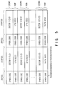
- the data generate circuit 14 includes an ECC (error correcting code) block data generate circuit 14a for converting ECC block format data as record data like the one shown in FIG. 2, which is supplied from an error correction circuit 32, into ECC block format data having ECC block synch. codes, as shown in FIG. 5, and a modulation circuit 14b for converting (modulating) the record data from the ECC block data generate circuit 14a according to the 8-15 code conversion scheme or the like.
- ECC error correcting code
- each ECC block synch. code has a 2-byte configuration, i.e., "0100000000000000 0100xxxxxxx00100” and is obtained by converting "175, 240" into an 8-15 code.
- This ECC block synch. code is different from a synch. code for ID detection.
- the ECC block format data in FIG. 5 represents a format actually recorded on an optical disk.
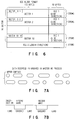
- Each sector of the ECC block format data in FIG. 6 has a 182 byte ⁇ 12 row configuration and consists of record data, a sector ID, and an ECC for the side direction.
- 2-byte synch. codes are added in units of 91 bytes, and a 2-byte synch. code is added to an ECC for the length direction for each 91 byte ⁇ 12 row unit.
- ECCs error correcting codes
- the error correction circuit 32 adds error correcting codes (ECCs 1 and 2) for the width and length directions and a sector ID to each 4Kbyte sector of 32Kbyte record data supplied from the control device 46 to form ECC block format data like the one shown in FIG. 6.
- ECCs 1 and 2 error correcting codes
- This cutting apparatus has a D/A converter 31 used to exchange data between the focusing control circuit 27, the tracking control circuit 28, the linear motor control circuit 8, and the CPU 30.
- the laser control circuit 13, the focusing control circuit 27, the tracking control circuit 28, the linear motor control circuit 8, the motor control circuit 4, the data generate circuit 14, and the like are controlled by the CPU 30 via a bus line 29.
- the CPU 30 performs predetermined operations in accordance with a cutting start command from an operation panel 34 and programs stored in a memory 33.
- a read only optical disk 51 is formed by injection molding or the like using this stamper.
- the cutting apparatus After the cutting apparatus completes a cutting process by melting the photoresist on the glass substrate 1b in accordance with record data for the entire surface of the substrate, developing and conducting processes are performed, thereby forming a glass master.
- a stamper consisting of nickel or the like is formed by electroplating or the like using this glass master.
- a rewritable optical disk (RAM) 52 having data recorded in only its grooves is formed by injection molding or the like using this stamper.
- the cutting apparatus After the cutting apparatus completes a cutting process by melting the photoresist on the glass substrate 1c in accordance with record data for the entire surface of the substrate, developing and conducting processes are performed, thereby forming a glass master.
- a stamper consisting of nickel or the like is formed by electroplating or the like using this glass master.
- a rewritable optical disk (RAM) 53 having data recorded in/on its grooves and lands is formed by injection molding or the like using this stamper.
- minute concave record marks corresponding to data are formed on the read only optical disk 51.
- the pit portions as record marks correspond to grooves, and the remaining portions correspond to lands.
- data is recorded in the above ECC block data unit (e.g., 38,688 bytes), and disk ID data is recorded as innermost ECC block data.
- This disk ID data includes data used to determine whether the disk is designed to record data in only grooves or both in grooves and on lands, data used to determine whether addresses on/from which data are to be recorded/reproduced are present on lands or in grooves, and the like.
- each ECC block address data (e.g., 66 bytes) is added to each ECC block data.
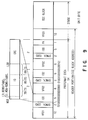
- each ECC block address data is constituted by the following areas: a 12-byte synch. code portion VFO1, two 8-byte synch. code portions VFO2, a 12-byte synch. code portion VFO3, three 2-byte synch. codes for ID detection, three 5-byte address portion IDs, and a 1-byte postamble PA.
- a consecutive data pattern (synch. code) for PLL locking is recorded in the synch. code portion VFO.
- a synch. code for ID detection is "0100000000000000 0100xxxxxxx00010", which is obtained by converting "119, 125, 128, 132, 138, 144, 152, 158, 164, 167, 171" into an 8-15 code.
- This synch. code for ID detection is different from a synch. code in ECC block data. In each address ID area, an ID such as an ECC block number consisting of 23 bits is recorded, together with the most significant bit (MSB) as a flag representing whether the corresponding ECC block can be rewritten, and a 2-byte error correcting code (CRC: Cyclic Redundancy Check).
- MSB most significant bit
- the postamble PA is used when the error correcting code for the address portion ID exceeds 2 bytes.
- disk ID data as ECC block data is recorded in the innermost groove of the rewritable optical disk (RAM) 53, and recording of data on the land corresponding to this innermost ECC block data is inhibited.
- the preformat data (e.g., 54 bytes) of a header portion is formed on the boundary between a groove and a land (adjacent to each other in the radial direction of the optical disk 1) for each ECC block data record area (e.g., 38,688 + 12 bytes).
- ECC block data record area e.g. 38,688 + 12 bytes
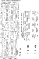
- the header portion is formed in forming grooves. As shown in FIG. 11, the header portion is constituted by a plurality of pits 101.
- the preformat pits 101 are formed with respect to grooves 102 in advance.
- the centers of the pits 101 are located on the same line of the tangent of the groove 102 to an adjacent land 103, as shown in FIG. 11.
- a pit string ID1 is the header portion of a groove 1
- a pit string ID2 is the header portion of a land 1
- a pit string ID3 is the header portion of a groove 2
- a pit string ID4 is the header portion of a land 2
- a pit string ID5 is the header portion of a groove 3
- a pit string ID6 is the header portion of a land 3.
- This disk ID data includes data used to determine whether the disk is designed to record data in only grooves or both in grooves and on lands, data used to determine whether addresses on/from which data are to be recorded/reproduced are present on lands or in grooves, and the like.
- the header portion corresponds to the above ECC block address data (see FIG. 9).
- a synch. code is recorded in the 12-byte synch. code portion VFO3 before recording of ECC block data, and PLL correction is performed by using the recorded synch. code in the reproduction mode.
- the rewritable optical disk (RAM) 52 is designed to record disk ID data as ECC block data in the innermost groove. Subsequently, as shown in FIG. 11, the preformat data (e.g., 54 bytes) of a header portion is formed in a groove for each ECC block data record area (e.g., 38,688 + 12 bytes).
- This disk ID data includes data used to determine whether the disk is designed to record data in only grooves or both in grooves and on lands, data used to determine whether addresses on/from which data are to be recorded/reproduced are present on lands or in grooves, and the like.
- the header portion corresponds to the above ECC block address data (see FIG. 9).
- a synch. code is recorded in the 12-byte synch. code portion VFO3 before recording of ECC block data, and PLL correction is performed by using the recorded synch. code in the reproduction mode.
- This signal is supplied to a data reproducing circuit 18.
- This data reproducing circuit 18 outputs an access permission signal with respect to an ECC block with a target ID for recording, or outputs reproduced data with respect to an ECC block with a target ID for reproduction.
- the data reproduced by the data reproducing circuit 18 is subjected to error correction using error correcting codes (ECCs) added by an error correction circuit 32.
- ECCs error correcting codes
- the resultant data is output to an optical disk control device 36 as an external device via an interface circuit 35.
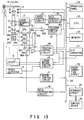
- a CPU 30A outputs a track ON/OFF signal, a tracking polarity switching signal, and a jump pulse to a tracking control circuit 28A, thereby to move a laser beam from a tracked land to the groove or from the groove to an adjacent land.
- the data reproducing circuit 18 comprises a comparator circuit 61, a header synch. code detection circuit 62, a header reading circuit 63, an ECC block synch. code detection circuit 64, and a data reading circuit 65.
- the comparator circuit 61 compares a reference signal with the sum signal of the outputs from the photodetection cells 24a to 24d of the photodetector 24, i.e., the changes in the reflectance of the pits (record data) formed in the grooves and lands of the tracks, thereby performing binarization.
- the comparator circuit 61 is constituted by a comparator and the like.
- the binary signal obtained by the comparator circuit 61 is supplied to the header synch. code detection circuit 62, the header reading circuit 63, the ECC block synch. code detection circuit 64, and the data reading circuit 65.
- the header synch. code detection circuit 62 detects the ID detection synch. codes "0100000000000000 0100xxxxxxx00010" of the header on the basis of the binary signal (binary data) corresponding to a predetermined number of bits, which is supplied from the comparator circuit 61.
- the header synch. code detection circuit 62 is constituted by a shift register for storing the binary data, a register for storing the ID detection synch. codes of the header, and a comparator for comparing the data in these registers.
- the detection signal from the header synch. code detection circuit 62 is supplied to the header reading circuit 63.
- the header reading circuit 63 reads the address portion ID of the binary data from the comparator circuit 61 in accordance with the detection signal from the header synch. code detection circuit 62. If this address portion ID coincides with the ID (to be accessed) supplied from the optical disk control device 36 as an external device, the header reading circuit 63 outputs an access permission signal.
- the header reading circuit 63 is constituted by a register for storing the binary data as the address portion ID from the comparator circuit 61, a register for storing the ID (to be accessed) supplied from the external device, and a comparator for comparing the data in these registers.
- the access permission signal from the header reading circuit 63 is supplied to the ECC block synch. code detection circuit 64, the data reading circuit 65, and the data generate circuit 14.
- the ECC block synch. code detection circuit 64 Upon reception of the access permission signal from the header reading circuit 63, the ECC block synch. code detection circuit 64 detects the ECC block synch. codes "0100000000000000 0100xxxxxxx00010" of the binary data, supplied from the comparator circuit 61, by the number corresponding to the number of bytes of the ECC block.
- the ECC block synch. code detection circuit 64 is constituted by a shift register for storing the binary data, a register for storing the ECC block synch. codes, and a comparator for comparing the data in these registers.
- the detection signal from the ECC block synch. code detection circuit 64 is supplied to the data reading circuit 65.
- the data reading circuit 65 Upon reception of the access permission signal from the header reading circuit 63, the data reading circuit 65 reads 91-byte binary data as reproduced data which is supplied from the comparator circuit 61 afterward, each time the data reading circuit 65 receives a detection signal from the ECC block synch. code detection circuit 64.
- the data reading circuit 65 is constituted by, e.g., a demodulation circuit, a binarization circuit, and the like.
- the demodulation circuit demodulates the binary data supplied from the comparator circuit 61 by inverse transformation of the 8-15 code.
- the binarization circuit binarizes the demodulated data in units of bytes.
- the resultant reproduced data is supplied to the error correction circuit 32.
- a laser control circuit 13 changes the intensity of a laser beam in accordance with a target optical disk.
- the data generate circuit 14 outputs record data to the laser control circuit 13 in the data recording mode in accordance with an access permission signal from the header reading circuit 63.
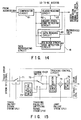
- the tracking control circuit 28A comprises change-over switches 71 and 72, a polarity inverting circuit 73, a phase compensation circuit 74, an adder portion 75, and a drive circuit 76.
- the change-over switch 71 is operated in accordance with a track ON/OFF signal (ON/OFF control of a tracking servo loop) from the CPU 30A, like the one shown in FIG. 16D.
- a track ON/OFF signal ON/OFF control of a tracking servo loop
- the change-over switch 71 outputs a track error signal, like the one shown in FIG. 16A, from a differential amplifier OP1 to the change-over switch 72 and the polarity inverting circuit 73.
- the change-over switch 72 is operated in accordance with a tracking switching signal (land/groove switching signal) from the CPU 30A, as shown in FIG. 16C.
- a tracking switching signal laand/groove switching signal
- the change-over switch 72 When the polarity of the tracking switching signal indicates a groove, the change-over switch 72 outputs a track error signal to the phase compensation circuit 74.
- the change-over switch 72 When the polarity of the tracking switching signal indicates a land, the change-over switch 72 outputs a track error signal whose polarity is inverted by the polarity inverting circuit 73 to the phase compensation circuit 74.
- the polarity inverting circuit 73 inverts the polarity of the track error signal supplied from the differential amplifier OP1 via the change-over switch 71.
- the output from the polarity inverting circuit 73 is supplied to the polarity inverting circuit 72.
- the phase compensation circuit 74 compensates the phase of the track error signal having positive polarity (positive phase) or opposite or negative polarity (opposite phase), which is supplied from the change-over switch 72, and outputs the resultant signal to the adder portion 75.
- the adder portion 75 adds the positive-polarity (positive-phase) track error signal or opposite-polarity (opposite-phase) track error signal which is supplied from the phase compensation circuit 74 upon compensation of the phase, with a jump pulse from the CPU 30A, like the one shown in FIG. 16B. The addition result is output as a track drive signal to the drive circuit 96.
- the drive circuit 76 drives a drive coil 11 in accordance with the track drive signal from the adder portion 75 to move an objective lens 10 in the tracking direction. That is, the tracking position of the laser beam is moved from a land to an adjacent groove in accordance with the jump pulse, like the one shown in FIG. 16B.
- the change-over switch 72 is switched to the polarity inverting circuit 73 side in accordance with a tracking polarity switching signal from the CPU 30A.
- the polarity of a track error signal is inverted by the polarity inverting circuit 73 via the change-over switch 71, and its phase is compensated by the phase compensation circuit 74 via the change-over switch 72.
- the resultant signal is supplied to the drive circuit 76.
- the drive circuit 76 drives the drive coil 11 to cause the laser beam passing through the objective lens 10 to track a land.
- the change-over switch 71 In moving the laser beam, the change-over switch 71 is turned off in accordance with the OFF state of a track ON/OFF signal from the CPU 30A. The tracking servo loop is released. At this time, a jump pulse from the CPU 30A is supplied to the drive circuit 76 via the adder portion 75. Upon reception of the jump pulse, the drive circuit 76 drives the drive coil 11 to move the irradiation position of the laser beam passing through the objective lens 10 from the current land to the outer (adjacent) groove. Upon completion of this movement, the change-over switch 71 is turned on again in accordance with the ON state of the track ON/OFF signal from the CPU 30A. The tracking servo loop is formed.
- the laser beam passing through the objective lens 10 is caused to track the groove.
- the change-over switch 72 is switched to the change-over switch 71 side in accordance with the tracking polarity switching signal from the CPU 30A.
- the phase of the track error signal is compensated by the phase compensation circuit 74 via the change-over switches 71 and 72.
- the resultant signal is used as a track drive signal and supplied to the drive circuit 76.
- the drive circuit 76 drives the drive coil 11 to cause the laser beam passing through the objective lens 10 to track the groove.
- the waveform of the jump pulse may be inverted to cause the laser beam to move to an inner (adjacent) groove.
- the CPU 30A causes the motor control circuit 4 to drive/control the motor 3 so as to rotate the optical disk at a predetermined rotational speed.
- the optical head 5 is then moved to a position as an initial position opposing the innermost peripheral portion of the optical disk 51 (52, 53), and focus lock-in is performed. More specifically, the CPU 30A outputs a reproduction control signal to the laser control circuit 13. As a result, the laser control circuit 13 irradiates a reproduction laser beam from the laser generate unit 19 in the optical head 5 onto the optical disk via the objective lens 10. The laser beam reflected by the optical disk 51 (52, 53) is guided to the photodetector 24 via the objective lens 10, the half prism 21, the condenser lens 22, and the cylindrical lens 23.
- the differential amplifier OP2 then obtains a focusing signal on the basis of the difference between the sum signal of outputs from the photodetection cells 24a and 24c of the photodetector 24 and the sum signal of outputs from the photodetection cells 24b and 24d of the photodetector 24, and outputs it to the focusing control circuit 27.
- the focusing control circuit 27 excites a drive coil 12 in accordance with the supplied focusing signal to move the objective lens 10, thereby focusing the laser beam irradiated onto the optical disk 51 (52, 53).
- the differential amplifier OP1 outputs the difference between the sum signal of the outputs from the photodetection cells 24a and 24d of the photodetector 24 and the sum signal of the outputs from the photodetection cells of the photodetector 24, as a track error signal, to the tracking control circuit 28A.
- the track error signal from the differential amplifier OP1 is output to the phase compensation circuit 74 via the change-over switches 71 and 72.
- the phase compensation circuit 74 performs phase compensation of the supplied track error signal, and outputs the resultant signal as a drive signal to the drive circuit 76 via the adder portion 75.
- the drive circuit 76 drives the objective lens 10 through the drive coil 11 in accordance with the supplied drive signal to perform tracking correction for fine movement of the laser beam irradiated on the optical disk 51 (52, 53) via the objective lens 10.
- the optical head 5 therefore irradiates the laser beam onto the innermost peripheral portion of the optical disk 51 (52, 53).
- the header reading circuit 63 reads an address portion ID. If this address portion ID coincides with the address ID of disk ID data (to be accessed) supplied from the optical disk control device 36 as an external device, an access permission signal is output to the ECC block synch. code detection circuit 64 and the data reading circuit 65.
- the data reading circuit 65 reads subsequent 91-byte data as reproduced data.
- the reproduced data is demodulated by inverse transformation of an 8-15 code using a demodulation circuit (not shown), and output to the error correction circuit 32.
- the data reading circuit 65 may read subsequent 91-byte data as reproduced data without using the header synch. code detection circuit 62 and the header reading circuit 63. In this case, no ECC block address is required.
- the error correction circuit 32 performs error correction by using error correcting codes (ECCs) added to the supplied reproduced data, and outputs the resultant data to the optical disk control device 36 as an external device via the interface circuit 35.
- ECCs error correcting codes
- disk ID data is supplied to the optical disk control device 36.
- the optical disk control device 36 discriminates, on the basis of the supplied disk ID data, whether the loaded optical disk is the read only optical disk 51, the rewritable optical disk (RAM) 52 designed to record data in only grooves, or the rewritable optical disk (RAM) 53 designed to record data in grooves and on lands. Upon discriminating that the optical disk is the optical disk 53, the optical disk control device 36 discriminates whether the access position is at a groove or land, and outputs these discrimination results and the address ID, at which recording or reproduction (access) is to be performed, to the CPU 30A.
- the CPU 30A changes the tracking switching signal to be output to the tracking control circuit 28A into a signal corresponding to a land only when receiving the discrimination result indicating that the access position is at a land.
- the change-over switch 72 is switched, and the track error signal from the differential amplifier OP1 is inverted by the polarity inverting circuit 73 via the change-over switch 71 and output to the phase compensation circuit 74.
- the tracking control circuit 28A performs tracking correction for fine movement of the laser beam in accordance with the polarity (opposite phase) corresponding to a land.
- the tracking position can be accurately changed from the groove or land to the land or groove.
- the rewritable optical disk (RAM) 53 has a structure in which the spiral land is formed adjacent to the spiral groove. Therefore, the groove and the land are prevented from being linked together.
- the second embodiment will exemplify a rewritable optical disk (RAM) 54 having a structure in which lands and grooves are alternately formed in units of rounds and linked together.
- RAM rewritable optical disk
- the same reference numerals in the second embodiment denote the same parts as in the first embodiment, and a detailed description thereof will be omitted.
- the optical disk 54 is formed near a header portion at a switching position for each round, as shown in FIGS. 18 and 19.
- a land or groove is switched to a groove or land.
- a land is formed continuously to a land before and after the header portion, while a groove is formed continuously to a groove, as shown in FIG. 11.
- a mark 110 indicating switching position from a land or groove to a groove to land is formed inside the innermost peripheral portion of the optical disk 54.
- the mark 110 is detected by a photosensor 111 arranged opposing the innermost peripheral portion of the optical disk 54 to store the position of the optical disk 54 in the circumferential direction.
- An detected output from the photosensor 111 is converted into a digital signal by an A/D converter 112 and supplied to a CPU 30A via a bus 29.
- a clock from a clock generator (not shown) is counted for each round of the optical disk 54.
- a detected signal is supplied from the photosensor 111.
- the CPU 30A stores a count value at the start of detecting the mark 110 and a count value at the end of detecting the mark 110 in a memory 2.
- the CPU 30A When a laser beam reaches the start position of the mark 110, the CPU 30A outputs a track OFF signal and a tracking polarity switching signal to a tracking control circuit 28A. When the laser beam passes the end position of the mark 110, the CPU 30A outputs a track ON signal to the tracking control circuit 28A.
- a change-over switch 72 is switched to a polarity inverting circuit 73 side in accordance with a tracking polarity switching signal from the CPU 30A.
- the polarity of a track error signal is inverted by the polarity inverting circuit 73 via a change-over switch 71, and its phase is compensated by a phase compensation circuit 74 via the change-over switch 72.
- the resultant signal is supplied to a drive circuit 76.
- the drive circuit 76 drives a drive coil 11 to cause the laser beam passing through the objective lens 10 to track a land.
- the CPU 30A When the laser beam reaches the start position of the mark 110, the CPU 30A outputs a track ON/OFF signal to turn off the change-over switch 71, thereby releasing a tracking servo loop.
- the CPU 30A outputs a tracking polarity switching signal to switch the change-over switch 72 to the change-over switch 71 side.
- the track ON/OFF signal from the CPU 30A is set ON again to turn on the change-over switch 71, thereby forming the tracking servo loop.
- the laser beam passing through the objective lens 10 is caused to track a groove.
- the change-over switch 72 is switched to the change-over switch 71 side in accordance with the tracking polarity switching signal from the CPU 30A.
- the phase of the track error signal is compensated by the phase compensation circuit 74 via the change-over switches 71 and 72.
- the resultant signal is used as a track drive signal and supplied to the drive circuit 76.
- the drive circuit 76 drives the drive coil 11 to cause the laser beam passing through the objective lens 10 to track the groove.
- the same operation is performed when the laser beam tracking a groove is caused to track a land in correspondence with the switching position of the mark 110.
- the CPU 30A causes a motor control circuit 4 to drive/control a motor 3 so as to rotate the optical disk 54 at a predetermined rotational speed.
- the CPU 30A detects the mark 110 in accordance with the detection signal from the photosensor 111, and stores, in the memory 2, a count value corresponding to the position of the optical disk 54 in the circumferential direction, i.e., count values corresponding to the start and end positions of the mark 110.
- An optical head 5 is then moved to a position as an initial position opposing the innermost peripheral portion of the optical disk 54, and focus lock-in is performed. More specifically, the CPU 30A outputs a reproduction control signal to a laser control circuit 13. As a result, the laser control circuit 13 irradiates a reproduction laser beam from a laser generate unit 19 in the optical head 5 onto the optical disk 54 via the objective lens 10. The laser beam reflected by the optical disk 54 is guided to a photodetector 24 via the objective lens 10, a half prism 21, a condenser lens 22, and a cylindrical lens 23.
- a differential amplifier OP2 then obtains a focusing signal on the basis of the difference between the sum signal of outputs from photodetection cells 24a and 24c of the photodetector 24 and the sum signal of outputs from photodetection cells 24b and 24d of the photodetector 24, and outputs it to a focusing control circuit 27.
- the focusing control circuit 27 excites a drive coil 12 in accordance with the supplied focusing signal to move the objective lens 10, thereby focusing the laser beam irradiated onto the optical disk 54.
- a differential amplifier OP1 outputs the difference between the sum signal of the outputs from the photodetection cells 24a and 24d of the photodetector 24 and the sum signal of the outputs from the photodetection cells of the photodetector 24, as a track error signal, to the tracking control circuit 28A.
- the track error signal from the differential amplifier OP1 is output to the phase compensation circuit 74 via the change-over switches 71 and 72.
- the phase compensation circuit 74 performs phase compensation of the supplied track error signal, and outputs the resultant signal as a drive signal to the drive circuit 76 via an adder portion 75.
- the drive circuit 76 drives the objective lens 10 through the drive coil 11 in accordance with the supplied drive signal to perform tracking correction for fine movement of the laser beam irradiated on the optical disk 54 via the objective lens 10.
- the optical head 5 therefore irradiates the laser beam onto the innermost peripheral portion of the optical disk 54.
- a read signal corresponding to the data on the innermost track is binarized by a comparator circuit 61 in a data reproducing circuit 18, and the binary data is supplied to a header synch.
- code detection circuit 62 a header reading circuit 63, an ECC block synch.
- code detection circuit 64 and a data reading circuit 65.
- the header reading circuit 63 reads an address portion ID. If this address portion ID coincides with the address ID of disk ID data (to be accessed) supplied from an optical disk control device 36 as an external device, an access permission signal is output to the ECC block synch. code detection circuit 64 and the data reading circuit 65.
- the data reading circuit 65 reads subsequent 91-byte data as reproduced data.
- the reproduced data is demodulated by inverse transformation of an 8-15 code using a demodulation circuit (not shown), and output to an error correction circuit 32.
- the data reading circuit 65 may read subsequent 91-byte data as reproduced data without using the header synch. code detection circuit 62 and the header reading circuit 63. In this case, no ECC block address is required.
- the error correction circuit 32 performs error correction by using error correcting codes (ECCs) added to the supplied reproduced data, and outputs the resultant data to the optical disk control device 36 as an external device via an interface circuit 35.
- ECCs error correcting codes
- disk ID data is supplied to the optical disk control device 36.
- the optical disk control device 36 discriminates, on the basis of the supplied disk ID data, whether the loaded optical disk is the read only optical disk 51, a rewritable optical disk (RAM) 52 designed to record data in only grooves, or a rewritable optical disk (RAM) 53 designed to record data in grooves and on lands. Upon discriminating that the optical disk is the optical disk 53, the optical disk control device 36 discriminates whether the access position is at a groove or land, and outputs these discrimination results and the address ID, at which recording or reproduction (access) is to be performed, to the CPU 30A.
- RAM rewritable optical disk
- RAM rewritable optical disk
- the CPU 30A changes the tracking switching signal to be output to the tracking control circuit 28A into a signal corresponding to a land only when receiving the discrimination result indicating that the access position is at a land.
- the change-over switch 72 is switched, and the track error signal from the differential amplifier OP1 is inverted by the polarity inverting circuit 73 via the change-over switch 72 and output to the phase compensation circuit 74.
- the tracking control circuit 28A performs tracking correction for fine movement of the laser beam in accordance with the polarity (opposite phase) corresponding to a land.
- the tracking position can be accurately changed from the groove or land to the land or groove.
Landscapes
- Engineering & Computer Science (AREA)
- Signal Processing (AREA)
- Optical Recording Or Reproduction (AREA)
- Moving Of The Head For Recording And Reproducing By Optical Means (AREA)
- Signal Processing For Digital Recording And Reproducing (AREA)
Applications Claiming Priority (3)
| Application Number | Priority Date | Filing Date | Title |
|---|---|---|---|
| JP20442995 | 1995-08-10 | ||
| JP204429/95 | 1995-08-10 | ||
| JP20442995A JP3707835B2 (ja) | 1995-08-10 | 1995-08-10 | 光ディスク装置 |
Publications (3)
| Publication Number | Publication Date |
|---|---|
| EP0759609A2 true EP0759609A2 (fr) | 1997-02-26 |
| EP0759609A3 EP0759609A3 (fr) | 1997-07-16 |
| EP0759609B1 EP0759609B1 (fr) | 2003-03-26 |
Family
ID=16490397
Family Applications (1)
| Application Number | Title | Priority Date | Filing Date |
|---|---|---|---|
| EP96112901A Expired - Lifetime EP0759609B1 (fr) | 1995-08-10 | 1996-08-09 | Appareil de disque optique, son circuit de commande de suivi de piste et procédé de changement de position de suivi de piste |
Country Status (5)
| Country | Link |
|---|---|
| US (1) | US5793722A (fr) |
| EP (1) | EP0759609B1 (fr) |
| JP (1) | JP3707835B2 (fr) |
| KR (1) | KR100243457B1 (fr) |
| DE (1) | DE69626903T2 (fr) |
Cited By (4)
| Publication number | Priority date | Publication date | Assignee | Title |
|---|---|---|---|---|
| EP0881632A3 (fr) * | 1997-05-27 | 1999-02-03 | Kabushiki Kaisha Toshiba | Disque optique et dispositif d'enregistrement/lecture d'informations utilisant ce disquek |
| EP1003163A4 (fr) * | 1998-06-04 | 2001-02-14 | Sony Corp | Support d'enregistrement optique |
| WO2004038710A1 (fr) * | 2002-10-23 | 2004-05-06 | Matsushita Electric Industrial Co., Ltd. | Lecteur de disque optique et son procede de commande |
| EP1184847A3 (fr) * | 2000-08-23 | 2004-07-07 | Pioneer Corporation | Dispositif de détection d'oscillation |
Families Citing this family (6)
| Publication number | Priority date | Publication date | Assignee | Title |
|---|---|---|---|---|
| EP0926664B1 (fr) * | 1997-12-26 | 2006-05-31 | Kabushiki Kaisha Toshiba | Disque optique et appareil de disque optique |
| KR100606680B1 (ko) * | 1999-07-28 | 2006-07-31 | 엘지전자 주식회사 | 광 기록매체에서의 트랙 점프 제어 방법 |
| JP2001126408A (ja) * | 1999-10-29 | 2001-05-11 | Sony Corp | 光学式回転記録媒体、アドレス情報記録方法、アドレス情報復元方法、光学式記録装置、光学式再生装置、および、光学式記録・再生装置 |
| KR100546309B1 (ko) * | 2002-12-28 | 2006-01-26 | 삼성전자주식회사 | 디브이디-램 디스크 드라이브에서의 자동 포즈 방법 |
| JP4615423B2 (ja) * | 2005-11-14 | 2011-01-19 | パナソニック株式会社 | トラックジャンピング走査制御装置およびトラック検索装置 |
| JP5168799B2 (ja) * | 2006-03-01 | 2013-03-27 | 日本電気株式会社 | インタフェース回路 |
Family Cites Families (9)
| Publication number | Priority date | Publication date | Assignee | Title |
|---|---|---|---|---|
| JPS5750330A (en) * | 1980-09-11 | 1982-03-24 | Matsushita Electric Ind Co Ltd | Optical recording and reproducing device |
| JPS59168939A (ja) * | 1983-03-16 | 1984-09-22 | Matsushita Electric Ind Co Ltd | デイスク記録再生装置 |
| JPS6366734A (ja) * | 1986-09-08 | 1988-03-25 | Fujitsu Ltd | 光デイスク装置 |
| JPH01169741A (ja) * | 1987-12-24 | 1989-07-05 | Nec Corp | トラック極性検出装置 |
| DE3916462A1 (de) * | 1989-05-20 | 1990-11-22 | Thomson Brandt Gmbh | Verfahren zum spurspringen |
| JPH056590A (ja) * | 1991-06-28 | 1993-01-14 | Toshiba Corp | 光磁気記録装置 |
| JP2633417B2 (ja) * | 1991-08-02 | 1997-07-23 | シャープ株式会社 | 光記録媒体駆動装置 |
| JP2860229B2 (ja) * | 1993-06-25 | 1999-02-24 | 株式会社ケンウッド | 光ディスク記録再生装置 |
| US5444682A (en) * | 1993-09-07 | 1995-08-22 | Matsushita Electric Industrial Co., Ltd. | Tracking control apparatus |
-
1995
- 1995-08-10 JP JP20442995A patent/JP3707835B2/ja not_active Expired - Lifetime
-
1996
- 1996-08-09 KR KR1019960033134A patent/KR100243457B1/ko not_active Expired - Lifetime
- 1996-08-09 EP EP96112901A patent/EP0759609B1/fr not_active Expired - Lifetime
- 1996-08-09 DE DE69626903T patent/DE69626903T2/de not_active Expired - Lifetime
- 1996-08-09 US US08/694,823 patent/US5793722A/en not_active Expired - Lifetime
Cited By (8)
| Publication number | Priority date | Publication date | Assignee | Title |
|---|---|---|---|---|
| EP0881632A3 (fr) * | 1997-05-27 | 1999-02-03 | Kabushiki Kaisha Toshiba | Disque optique et dispositif d'enregistrement/lecture d'informations utilisant ce disquek |
| US6172961B1 (en) | 1997-05-27 | 2001-01-09 | Kabushiki Kaisha Toshiba | Optical recording disk having land and groove continuously alternated in spiral tracks |
| EP1003163A4 (fr) * | 1998-06-04 | 2001-02-14 | Sony Corp | Support d'enregistrement optique |
| US6800348B2 (en) | 1998-06-04 | 2004-10-05 | Sony Corporation | Optical recording medium |
| EP1184847A3 (fr) * | 2000-08-23 | 2004-07-07 | Pioneer Corporation | Dispositif de détection d'oscillation |
| WO2004038710A1 (fr) * | 2002-10-23 | 2004-05-06 | Matsushita Electric Industrial Co., Ltd. | Lecteur de disque optique et son procede de commande |
| US7088662B2 (en) | 2002-10-23 | 2006-08-08 | Matsushita Electric Industrial Co., Ltd. | Optical disc drive and method for controlling the same |
| CN1300785C (zh) * | 2002-10-23 | 2007-02-14 | 松下电器产业株式会社 | 光盘驱动器及其控制方法 |
Also Published As
| Publication number | Publication date |
|---|---|
| DE69626903T2 (de) | 2004-01-29 |
| EP0759609A3 (fr) | 1997-07-16 |
| KR100243457B1 (ko) | 2000-02-01 |
| DE69626903D1 (de) | 2003-04-30 |
| JP3707835B2 (ja) | 2005-10-19 |
| US5793722A (en) | 1998-08-11 |
| KR970012386A (ko) | 1997-03-29 |
| JPH0954963A (ja) | 1997-02-25 |
| EP0759609B1 (fr) | 2003-03-26 |
Similar Documents
| Publication | Publication Date | Title |
|---|---|---|
| RU2174716C2 (ru) | Устройство с оптическим диском и способ осуществления замены для оптического диска | |
| US5963522A (en) | Optical disk device and method for detecting and replacing a defective sector within a block containing recording data and error correction data on an optical disk | |
| EP0759609B1 (fr) | Appareil de disque optique, son circuit de commande de suivi de piste et procédé de changement de position de suivi de piste | |
| EP0881632B1 (fr) | Disque optique et système d'enregistrement/lecture d'informations | |
| EP0759611B1 (fr) | Appareil à disque optique et méthode de lecture pour différentes sortes de disques | |
| KR20010031105A (ko) | 멀티 빔 광 디스크 판독 방법 및 장치 | |
| JP3959147B2 (ja) | 光ディスク、光ディスク再生装置、光ディスク再生方法、及び光ディスク記録方法 | |
| JP3959149B2 (ja) | 光ディスク、光ディスク再生装置、光ディスク再生方法、及び光ディスク記録方法 | |
| JP3707834B2 (ja) | 光ディスク装置 | |
| US5544134A (en) | Optical disk apparatus for reading data from zones of an optical disk using different frequency clocks | |
| JP3875399B2 (ja) | 光ディスク装置のトラッキング方法とdvd−ramドライブ装置のトラッキング方法 | |
| JP3762027B2 (ja) | 光ディスク、光ディスク再生装置、光ディスク再生方法、及び光ディスク記録方法 | |
| JP3762029B2 (ja) | 光ディスク、光ディスク再生装置、光ディスク再生方法、及び光ディスク記録方法 | |
| JP3762028B2 (ja) | 光ディスク、光ディスク再生装置、光ディスク再生方法、及び光ディスク記録方法 | |
| JP3908347B2 (ja) | 光ディスク再生装置及び光ディスク再生方法 | |
| JP3959148B2 (ja) | 光ディスク、光ディスク再生装置、光ディスク再生方法、及び光ディスク記録方法 | |
| JPH0954661A (ja) | 光ディスクと光ディスクの作成装置 | |
| JP3872887B2 (ja) | 光ディスク装置 | |
| JPH0955034A (ja) | 光ディスク装置および光ディスク | |
| JPH1186462A (ja) | 光ディスク装置及びデータ再生方法 | |
| JPH10247325A (ja) | データ記録装置と光ディスク装置のトラッキング方法と光ディスク装置の信号処理方法 | |
| JPH08255351A (ja) | 情報記録再生装置 | |
| JPH11213392A (ja) | 光ディスク及び光ディスク装置 | |
| JPH1153737A (ja) | 光ディスク装置 | |
| JPH1064168A (ja) | データ記録装置 |
Legal Events
| Date | Code | Title | Description |
|---|---|---|---|
| PUAI | Public reference made under article 153(3) epc to a published international application that has entered the european phase |
Free format text: ORIGINAL CODE: 0009012 |
|
| 17P | Request for examination filed |
Effective date: 19960906 |
|
| AK | Designated contracting states |
Kind code of ref document: A2 Designated state(s): DE FR GB NL |
|
| PUAL | Search report despatched |
Free format text: ORIGINAL CODE: 0009013 |
|
| AK | Designated contracting states |
Kind code of ref document: A3 Designated state(s): DE FR GB NL |
|
| 17Q | First examination report despatched |
Effective date: 20010625 |
|
| GRAH | Despatch of communication of intention to grant a patent |
Free format text: ORIGINAL CODE: EPIDOS IGRA |
|
| GRAH | Despatch of communication of intention to grant a patent |
Free format text: ORIGINAL CODE: EPIDOS IGRA |
|
| GRAA | (expected) grant |
Free format text: ORIGINAL CODE: 0009210 |
|
| AK | Designated contracting states |
Designated state(s): DE FR GB NL |
|
| PG25 | Lapsed in a contracting state [announced via postgrant information from national office to epo] |
Ref country code: NL Free format text: LAPSE BECAUSE OF FAILURE TO SUBMIT A TRANSLATION OF THE DESCRIPTION OR TO PAY THE FEE WITHIN THE PRESCRIBED TIME-LIMIT Effective date: 20030326 |
|
| REG | Reference to a national code |
Ref country code: GB Ref legal event code: FG4D |
|
| REF | Corresponds to: |
Ref document number: 69626903 Country of ref document: DE Date of ref document: 20030430 Kind code of ref document: P |
|
| NLV1 | Nl: lapsed or annulled due to failure to fulfill the requirements of art. 29p and 29m of the patents act | ||
| ET | Fr: translation filed | ||
| PLBE | No opposition filed within time limit |
Free format text: ORIGINAL CODE: 0009261 |
|
| STAA | Information on the status of an ep patent application or granted ep patent |
Free format text: STATUS: NO OPPOSITION FILED WITHIN TIME LIMIT |
|
| 26N | No opposition filed |
Effective date: 20031230 |
|
| PGFP | Annual fee paid to national office [announced via postgrant information from national office to epo] |
Ref country code: FR Payment date: 20140808 Year of fee payment: 19 |
|
| PGFP | Annual fee paid to national office [announced via postgrant information from national office to epo] |
Ref country code: DE Payment date: 20150804 Year of fee payment: 20 Ref country code: GB Payment date: 20150805 Year of fee payment: 20 |
|
| REG | Reference to a national code |
Ref country code: FR Ref legal event code: ST Effective date: 20160429 |
|
| REG | Reference to a national code |
Ref country code: DE Ref legal event code: R071 Ref document number: 69626903 Country of ref document: DE |
|
| PG25 | Lapsed in a contracting state [announced via postgrant information from national office to epo] |
Ref country code: FR Free format text: LAPSE BECAUSE OF NON-PAYMENT OF DUE FEES Effective date: 20150831 |
|
| REG | Reference to a national code |
Ref country code: GB Ref legal event code: PE20 Expiry date: 20160808 |
|
| PG25 | Lapsed in a contracting state [announced via postgrant information from national office to epo] |
Ref country code: GB Free format text: LAPSE BECAUSE OF EXPIRATION OF PROTECTION Effective date: 20160808 |