EP0759640B1 - Halbleiter-Übergitter-Oszillator und Verfahren zur Herstellung und zum Betrieb - Google Patents
Halbleiter-Übergitter-Oszillator und Verfahren zur Herstellung und zum Betrieb Download PDFInfo
- Publication number
- EP0759640B1 EP0759640B1 EP96113185A EP96113185A EP0759640B1 EP 0759640 B1 EP0759640 B1 EP 0759640B1 EP 96113185 A EP96113185 A EP 96113185A EP 96113185 A EP96113185 A EP 96113185A EP 0759640 B1 EP0759640 B1 EP 0759640B1
- Authority
- EP
- European Patent Office
- Prior art keywords
- semiconductor
- layers
- layer
- oscillator
- superlattice
- Prior art date
- Legal status (The legal status is an assumption and is not a legal conclusion. Google has not performed a legal analysis and makes no representation as to the accuracy of the status listed.)
- Expired - Lifetime
Links
- 239000003362 semiconductor superlattice Substances 0.000 title claims description 14
- 238000000034 method Methods 0.000 title claims description 10
- 238000004519 manufacturing process Methods 0.000 title claims description 4
- 230000010355 oscillation Effects 0.000 claims description 68
- 239000004065 semiconductor Substances 0.000 claims description 23
- 230000004888 barrier function Effects 0.000 claims description 19
- 239000000758 substrate Substances 0.000 claims description 11
- 239000000463 material Substances 0.000 claims description 10
- 238000009826 distribution Methods 0.000 claims description 8
- 230000002459 sustained effect Effects 0.000 claims description 8
- 230000008878 coupling Effects 0.000 claims description 4
- 238000010168 coupling process Methods 0.000 claims description 4
- 238000005859 coupling reaction Methods 0.000 claims description 4
- 230000000737 periodic effect Effects 0.000 claims description 3
- 239000003990 capacitor Substances 0.000 claims 1
- 150000001875 compounds Chemical class 0.000 claims 1
- 239000010410 layer Substances 0.000 description 43
- 239000000523 sample Substances 0.000 description 18
- 229910001218 Gallium arsenide Inorganic materials 0.000 description 15
- 230000005684 electric field Effects 0.000 description 10
- 230000000694 effects Effects 0.000 description 8
- 238000009825 accumulation Methods 0.000 description 7
- 238000005424 photoluminescence Methods 0.000 description 7
- 239000000969 carrier Substances 0.000 description 5
- 239000000203 mixture Substances 0.000 description 5
- 230000015572 biosynthetic process Effects 0.000 description 4
- 238000005259 measurement Methods 0.000 description 4
- 230000007246 mechanism Effects 0.000 description 4
- 238000000103 photoluminescence spectrum Methods 0.000 description 4
- XUIMIQQOPSSXEZ-UHFFFAOYSA-N Silicon Chemical compound [Si] XUIMIQQOPSSXEZ-UHFFFAOYSA-N 0.000 description 3
- 230000005540 biological transmission Effects 0.000 description 3
- 230000008859 change Effects 0.000 description 3
- 230000005284 excitation Effects 0.000 description 3
- 230000033001 locomotion Effects 0.000 description 3
- 230000003287 optical effect Effects 0.000 description 3
- 230000008569 process Effects 0.000 description 3
- 230000002441 reversible effect Effects 0.000 description 3
- 238000005070 sampling Methods 0.000 description 3
- 229910052710 silicon Inorganic materials 0.000 description 3
- 239000010703 silicon Substances 0.000 description 3
- 238000001228 spectrum Methods 0.000 description 3
- 238000012546 transfer Methods 0.000 description 3
- 229910000530 Gallium indium arsenide Inorganic materials 0.000 description 2
- 239000002800 charge carrier Substances 0.000 description 2
- 230000001427 coherent effect Effects 0.000 description 2
- 238000002474 experimental method Methods 0.000 description 2
- 230000012010 growth Effects 0.000 description 2
- 238000005304 joining Methods 0.000 description 2
- 230000003534 oscillatory effect Effects 0.000 description 2
- 230000003068 static effect Effects 0.000 description 2
- 230000001052 transient effect Effects 0.000 description 2
- 229910000980 Aluminium gallium arsenide Inorganic materials 0.000 description 1
- 230000001133 acceleration Effects 0.000 description 1
- 230000003321 amplification Effects 0.000 description 1
- 230000008901 benefit Effects 0.000 description 1
- 238000011088 calibration curve Methods 0.000 description 1
- 230000003247 decreasing effect Effects 0.000 description 1
- 230000001419 dependent effect Effects 0.000 description 1
- 230000001747 exhibiting effect Effects 0.000 description 1
- 238000002347 injection Methods 0.000 description 1
- 239000007924 injection Substances 0.000 description 1
- 238000011835 investigation Methods 0.000 description 1
- 230000004807 localization Effects 0.000 description 1
- 238000012544 monitoring process Methods 0.000 description 1
- 238000003199 nucleic acid amplification method Methods 0.000 description 1
- 238000000628 photoluminescence spectroscopy Methods 0.000 description 1
- 230000001902 propagating effect Effects 0.000 description 1
- 230000005701 quantum confined stark effect Effects 0.000 description 1
- 230000005855 radiation Effects 0.000 description 1
- 230000006798 recombination Effects 0.000 description 1
- 238000005215 recombination Methods 0.000 description 1
- 230000004044 response Effects 0.000 description 1
- 239000002356 single layer Substances 0.000 description 1
- 239000000243 solution Substances 0.000 description 1
- 125000006850 spacer group Chemical class 0.000 description 1
- 238000012360 testing method Methods 0.000 description 1
- 238000001039 wet etching Methods 0.000 description 1
Images





Classifications
-
- B—PERFORMING OPERATIONS; TRANSPORTING
- B82—NANOTECHNOLOGY
- B82Y—SPECIFIC USES OR APPLICATIONS OF NANOSTRUCTURES; MEASUREMENT OR ANALYSIS OF NANOSTRUCTURES; MANUFACTURE OR TREATMENT OF NANOSTRUCTURES
- B82Y30/00—Nanotechnology for materials or surface science, e.g. nanocomposites
-
- B—PERFORMING OPERATIONS; TRANSPORTING
- B82—NANOTECHNOLOGY
- B82Y—SPECIFIC USES OR APPLICATIONS OF NANOSTRUCTURES; MEASUREMENT OR ANALYSIS OF NANOSTRUCTURES; MANUFACTURE OR TREATMENT OF NANOSTRUCTURES
- B82Y10/00—Nanotechnology for information processing, storage or transmission, e.g. quantum computing or single electron logic
-
- H—ELECTRICITY
- H03—ELECTRONIC CIRCUITRY
- H03B—GENERATION OF OSCILLATIONS, DIRECTLY OR BY FREQUENCY-CHANGING, BY CIRCUITS EMPLOYING ACTIVE ELEMENTS WHICH OPERATE IN A NON-SWITCHING MANNER; GENERATION OF NOISE BY SUCH CIRCUITS
- H03B7/00—Generation of oscillations using active element having a negative resistance between two of its electrodes
- H03B7/12—Generation of oscillations using active element having a negative resistance between two of its electrodes with frequency-determining element comprising distributed inductance and capacitance
- H03B7/14—Generation of oscillations using active element having a negative resistance between two of its electrodes with frequency-determining element comprising distributed inductance and capacitance active element being semiconductor device
-
- H—ELECTRICITY
- H10—SEMICONDUCTOR DEVICES; ELECTRIC SOLID-STATE DEVICES NOT OTHERWISE PROVIDED FOR
- H10D—INORGANIC ELECTRIC SEMICONDUCTOR DEVICES
- H10D62/00—Semiconductor bodies, or regions thereof, of devices having potential barriers
- H10D62/80—Semiconductor bodies, or regions thereof, of devices having potential barriers characterised by the materials
- H10D62/81—Semiconductor bodies, or regions thereof, of devices having potential barriers characterised by the materials of structures exhibiting quantum-confinement effects, e.g. single quantum wells; of structures having periodic or quasi-periodic potential variation
- H10D62/815—Semiconductor bodies, or regions thereof, of devices having potential barriers characterised by the materials of structures exhibiting quantum-confinement effects, e.g. single quantum wells; of structures having periodic or quasi-periodic potential variation of structures having periodic or quasi-periodic potential variation, e.g. superlattices or multiple quantum wells [MQW]
- H10D62/8161—Semiconductor bodies, or regions thereof, of devices having potential barriers characterised by the materials of structures exhibiting quantum-confinement effects, e.g. single quantum wells; of structures having periodic or quasi-periodic potential variation of structures having periodic or quasi-periodic potential variation, e.g. superlattices or multiple quantum wells [MQW] potential variation due to variations in composition or crystallinity, e.g. heterojunction superlattices
- H10D62/8162—Semiconductor bodies, or regions thereof, of devices having potential barriers characterised by the materials of structures exhibiting quantum-confinement effects, e.g. single quantum wells; of structures having periodic or quasi-periodic potential variation of structures having periodic or quasi-periodic potential variation, e.g. superlattices or multiple quantum wells [MQW] potential variation due to variations in composition or crystallinity, e.g. heterojunction superlattices having quantum effects only in the vertical direction, i.e. layered structures having quantum effects solely resulting from vertical potential variation
- H10D62/8164—Semiconductor bodies, or regions thereof, of devices having potential barriers characterised by the materials of structures exhibiting quantum-confinement effects, e.g. single quantum wells; of structures having periodic or quasi-periodic potential variation of structures having periodic or quasi-periodic potential variation, e.g. superlattices or multiple quantum wells [MQW] potential variation due to variations in composition or crystallinity, e.g. heterojunction superlattices having quantum effects only in the vertical direction, i.e. layered structures having quantum effects solely resulting from vertical potential variation comprising only semiconductor materials
-
- H—ELECTRICITY
- H10—SEMICONDUCTOR DEVICES; ELECTRIC SOLID-STATE DEVICES NOT OTHERWISE PROVIDED FOR
- H10D—INORGANIC ELECTRIC SEMICONDUCTOR DEVICES
- H10D8/00—Diodes
- H10D8/70—Tunnel-effect diodes
- H10D8/755—Resonant tunneling diodes [RTD]
Definitions
- the invention relates to a semiconductor superlattice oscillator, to a method of manufacturing a semiconductor oscillator and to a method of operating a semiconductor superlattice oscillator.
- the diode needs to have a certain minimum length because the electrons must be accelerated before they can make a transfer to higher valleys. Because the acceleration region mainly acts as a series resistance which dissipates power, this reduces the efficiency of the Gunn diodes.
- Double barrier resonant tunnelling diodes are also used for high frequency oscillations and indeed currently hold the record for high-frequency generation. They are characterised by low output power and low noise.
- IMPATT diodes so far deliver the greatest power of all diode generators (i.e. several watts in the microwave range).
- the noise of the injected current is multiplied by the same factor as the current.
- the multiplication process itself is of stochastic nature and adds extra noise.
- Gunn diodes are also known for having rather high noise levels, due to the inevitably high carrier temperature which is necessary for scattering into higher valleys of the band structures.
- a superlattice structure according to the preamble of claim 1 is known from Hadjazi et al. (Electron. Lett. 27(12), 1101-1103 (1991)). This superlattice structure is of the same type as the ones by Le Person et al. and Hadjaz et al. mentioned above.
- DE-AS 20 08 043 and the closely related DE-AS 20 14 677 are concerned with the coherent oscillation of charge carriers.
- the carriers are expected to oscillate in momentum space (K-space) as a result of a small applied field.
- K-space momentum space
- This field must be sufficiently small that, for the particular component and its parameters, no Stark localisation of electrons occurs, i.e. the minibands do not split up into discrete levels for each quantum well.
- the Bloch oscillator It is fundamental for the Bloch oscillator that the electric field is constant inside the superlattice structure. This is, however, only the case when no excess charge carriers are present. This is a dilemma and explains why oscillators of this kind have not been commercially realised. The dilemma is as follows:
- the object of the present invention is to provide a universally applicable novel constructional principle for oscillator elements.
- the principle should make it possible to realise oscillator elements having frequencies in a large frequency range from a few Hz up to a few hundred GHz by the freedom provided by the principle in the choice of parameters such as the barrier thickness, quantum well thickness, doping and length of the samples of the oscillator elements.
- the present invention provides a semiconductor superlattice oscillator comprising a semiconductor substrate having, in sequence, a first N-layer deposited directly or indirectly on the substrate, a superlattice structure comprising alternating pairs of semiconductor layers of materials of first and second band gaps deposited on said N-layer, there being preferably a minimum of ten and in particular more than twenty such layer pairs, and a second N-layer deposited on said superlattice structure (further layers being optionally also possible), there being first and second means for contacting said first and second layers respectively, characterised in that the superlattice layers are of a thickness such that energy quantisation in the form of subbands and resonant tunnelling between subbands of adjacent well layers takes place; and in that the doping density in the well layers is selected so that sustained oscillations of the field distribution inside the superlattice structure, and thus of the output current, occur.
- the invention is thus based on the concept of an oscillator element which functions on the basis of resonant tunnelling in semiconductor superlattice structures.
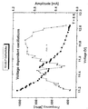
- the oscillation frequency depends on the tunnelling time through the barriers of the superlattice and on the number of periods (i.e. to the length of the device) and can be varied over a wide range from the kHz range up to several hundred GHz. These intrinsic frequencies can, moreover, be tuned through certain ranges within a system by variation of the applied voltage. For various subband resonances frequencies result which increase with the coupling strength.
- responsible for the oscillations are field inhomogeneities which arise through the oscillator elements and which arise as a result of the strongly non-linear transmission characteristic due to the resonant tunnelling.
- the present invention exploits travelling field inhomogeneities to produce a high quality (high Q-factor), electrically stimulated, sustained oscillation of tunable frequency.
- the oscillator of the present invention is based on the realisation that an alternative type of oscillation is possible, determined by the transit time of electrons through the whole structure. This transit time is determined by the length of the superlattice structure and the average drift velocity of the carriers which can be modulated by the externally applied voltage. For this to be achieved it is necessary for the 2D-doping density in the well layers to lie within certain limits. Above the upper limit static inhomogeneous field domains arise and the effect of the present invention is not observed. Below the lower limit broad undefined inhomogeneities arise and the effect is again no longer present. Stable inhomogeneous field oscillations only occur between these limits.
- the precise doping density cannot be given as a numerical value since it depends on the barrier width, the well width, the temperature, the sample quality, the sample length and the composition which determines the barrier height. It is, however, possible to give a guide to the selection of the required doping density. It is known that an accumulation of electrons occurs at an electrical field discontinuity, i.e. at positions where the field is not constant. The doping density should be chosen such that the 2D electron accumulation layer between the two fields is larger than the doping density by a factor of the order of 5 : 100. It cannot, however, be ruled out that with some structures the optimum will be found outside of this range. A rule of thumb of the determination of the doping density is as follows:
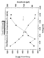
- One particularly important advantage of the semiconductor superlattice oscillator of the present invention is that it is tunable over a large frequency range in a very simple manner, namely by a variation of the applied potential difference.
- the invention can thus be used as a tunable oscillator.
- the oscillator frequency is set by incorporating the diode into an oscillator circuit, measuring the frequency of the oscillation, ablating the diode by a laser while in operation to change its length and its frequency of oscillation. Once this process is completed the frequency of oscillation is fixed.
- the temperature dependence of the tuning curve permits the generator to be used as a temperature sensor.
- the temperature can be read off from a calibration curve relating the frequency generated to a specific predetermined potential difference.
- the present invention recognises that resonant tunnelling can be used to produce an extremely effective semiconductor oscillator.
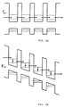
- the present invention exploits periodically returning field inhomogeneities in the superlattice which form the basis for the current oscillation - in similar manner to the Gunn effect.
- the field inhomogeneities are generated by the non-linear transmission characteristic v(F) of the superlattice, in particular in the region of negative differential conductivity (NDV).
- NDV negative differential velocity
- Time-resolved photoluminescence (PL) measurements demonstrate that the oscillations are due to the motion of charge accumulated at the domain boundary between two electric field domains.
- the frequency of the oscillation depends strongly on the barrier widths and, thus, on the tunnelling times.
- the domain regime ceases to be stable and self-generated oscillations occur.
- the oscillations are attributed to a periodic motion of the domain boundary over a few periods of the superlattice.
- the speed of the propagating charge accumulation layer in the SL is limited by the tunnelling time. Accordingly, the frequency of the oscillation increases with increasing tunnelling probability from a few hundred kHz into the MHz region.
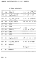
- SL samples Two SL samples will now be discussed, hereafter referred to as 9/4 and 13.3/2.7 according to their SL parameters.
- an undoped GaAs spacer of 25 nm thickness.
- This superlattice is followed by a 2.7nm AlAs undoped layer for symmetry reasons, which is usual when growing superlattices.
- On top of this layer there is then grown a further 25nm undoped GaAs layer, again for reasons of symmetry.
- a second sample was grown with a superlattice having forty periods of 4 nm thick barrier layers and 9 nm thick well layers in the same material system.
- the samples were processed by wet etching into mesas of 120 ⁇ m diameter (9/4) and 200 ⁇ m diameter (13.3/2.7).
- AuGe/Ni contacts 18, 20 evaporated on top and on the substrate side.
- the circular top contacts of 70 ⁇ m diameter leave a large part of the mesas uncovered to allow for optical access.
- All experiments were performed at 5 K in a He-Flow cryostat with high frequency coaxial cables with a bandwidth of 20 GHz.
- the current voltage traces were recorded using a Hewlett Packard (HP) 3245A voltage source and a HP3458A multimeter to measure the time averaged current.
- the time-resolved current was detected with a Tektronix sampling oscilloscope CSA 803 using the GHz sampling head SD-32.
- the samples are incorporated into an oscillator circuit, for example, as shown in Fig. 1B.
- the choke 22 is simply provided to isolate the oscillator from the voltage source 24 and is dimensioned so that it no longer transmits the lowest frequency of interest.
- the connection lines 26 used have 50 Ohm impedance for matching to the 50 Ohm input impedance of the attached circuit which comprises a sampling oscilloscope 28 in this test arrangement. All the cables used were 50 Ohm SMA cables with a maximum frequency of 20 GHz.
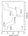
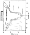
- Fig. 2 shows the current voltage (I-V) characteristics of the two samples at 5° K. Both structures exhibit two plateau regions in forward (+) and reverse (-) bias (here, forward denotes positive voltage at the top contact on the mesa so that the electrons are injected from the substrate side). The lower and upper plateaus begin at the current maximum corresponding to, respectively, tunnelling between the lowest subbands of adjacent wells (C1-C1 tunnelling) and C1-C2 tunnelling (C i denotes the i th electronic subband). For details on the plateau formation see [9, 10]. While the lower plateau of sample 9/4 in reverse bias shows the well understood series of current branches [11], all other plateaus are more or less flat revealing no direct sign of domain formation. Particularly interesting is the unexpected asymmetry in the I-V characteristic of sample 9/4, which is inconsistent with the symmetric growth sequence (n + -n-n + diodes).
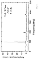
- Fig. 3(a) shows oscillations in sample 9/4 at +1 V. In this plateau the current oscillates at approximately 700 kHz, but the frequency increases to about 10 MHz in the upper plateau as shown in Fig. 3(b). This increase is due to the fact that the transmission probability at -8 V is governed by the C1-C2 tunnelling resonance which is much stronger than that for C1-C2, which controls the current in the lower plateau. Consistent with this interpretation, the current shown in Fig. 3(c) oscillates at an even higher frequency because the thinner barriers (2.7 nm) give rise to much shorter tunnelling times.
- Fig. 5(a) shows the zero-field and time-resolved PL spectra exhibiting a peak due to the recombination of electrons with heavy holes. Due to the quantum confined Stark effect, the PL emission from the quantum wells in an electric field shifts to the red with increasing field. Hence, measurements of the PL energy allows one to estimate the field strength in the superlattice. A Stark-splitted PL line indicates that there are two different field strengths present inside the SL [12]. Since the intensity of the emission is proportional to the length of the corresponding field domain, it is possible to obtain a rough estimate of this value. In experiments carried out by the inventors the excitation density was chosen, to be sufficiently small that the current oscillation was not perturbed.
- the time-resolved PL spectra shown in Fig. 5(a) were recorded at -8 V by triggering the streak camera on the current oscillation of Fig. 3(b). It should be noted that the time-resolved spectra are red-shifted with respect to the zero-field PL line indicating that a strong electric field is acting on the SL.
- the spectrum at 230 ns (peaked at 1,560 eV) and the spectrum at 275 ns (peaked at 1,565 eV) correspond to the current minima and maxima respectively.
- the trace at an intermediate time (250 ns) displays emission from both domain regions manifesting itself in the broader lineshape.
- the SL oscillation frequency can be significantly increased by reducing the barrier width. While higher frequencies can possibly be achieved by appropriately controlling the SL parameters, it remains to be seen that the instability allows frequencies beyond the GHz range.
- strongly coupled samples have recently been shown to exhibit THz Bloch oscillations [14]. While the oscillations underlying the present teaching are very different in nature it is possible that Bloch oscillations may constitute a frequency limit for the domain oscillations.
Landscapes
- Engineering & Computer Science (AREA)
- Chemical & Material Sciences (AREA)
- Nanotechnology (AREA)
- Physics & Mathematics (AREA)
- Crystallography & Structural Chemistry (AREA)
- Composite Materials (AREA)
- Condensed Matter Physics & Semiconductors (AREA)
- General Physics & Mathematics (AREA)
- Materials Engineering (AREA)
- Mathematical Physics (AREA)
- Theoretical Computer Science (AREA)
- Bipolar Transistors (AREA)
Claims (10)
- Halbleiterübergitteroszillator umfassend ein Halbleitersubstrat (10) mit, in der Reihenfolge, eine erste N-Schicht (12), die direkt oder indirekt auf dem Substrat (10) abgeschieden ist, einer auf der N-Schicht (12) abgeschiedenen Übergitterstruktur (14), die alternierende Paare von Halbleiterschichten aus Materialien mit einer ersten und einer zweiten Bandlücke umfasst, wobei es vorzugsweise ein Minimum von zehn und insbesondere mehr als zwanzig solcher Schichtpaare gibt, und einer zweiten N-Schicht (16), die auf der Übergitterstruktur (14) abgeschieden ist, wobei auch weitere Schichten optional möglich sind, wobei es ein erstes und ein zweites Mittel (18, 20) zum Kontaktieren jeweils der ersten und der zweiten Schicht (12, 16) gibt, dadurch gekennzeichnet, dass die Übergitterschichten eine Dicke derart aufweisen, dass eine Energiequantisierung in der Form von Subbändem und resonantes Tunneln zwischen Subbändern benachbarter Topfschichten stattfindet, und dass die Dotierdichte in den Topfschichten so gewählt ist, dass aufrechterhaltene Oszillationen der Feldverteilung im Inneren der Übergitterstruktur (14) und somit des Ausgangsstroms auftreten.
- Halbleiteroszillator nach Anspruch 1, dadurch gekennzeichnet, dass die Dotierung innerhalb eines zentralen Bereiches jeder Topfschicht, nicht aber in den Bereichen bewirkt ist, die direkt an die Barrierenschichten angrenzen.
- Halbleiteroszillator nach Anspruch 1, dadurch gekennzeichnet, dass Mittel (22 - 26) vorgesehen sind, um einen Potentialunterschied einer solchen Größe an das erste und zweite Kontaktmittel (18, 20) anzulegen, dass aufrechterhaltene Oszillationen aufgrund von resonantem Tunneln stattfinden.
- Halbleiteroszillator nach einem der vorherigen Ansprüche, wobei das ausgewählte Halbleitermaterialsystem ein beliebiges der Materialsysteme ist, bei denen eine periodische Modulation des Leitungsbandes erreichbar ist, zum Beispiel ein Verbindungshalbleiter mit einer III-Voder II-VI-Zusammensetzung.
- Halbleiteroszillator nach einem der vorherigen Ansprüche, dadurch gekennzeichnet, dass ein Kondensator vorgesehen ist, um die Oszillation des Halbleiteroszillators auszukoppeln, und dass der Kondensator durch eine Platte mit einem der ersten und zweiten Kontaktmittel (18, 20) und durch seine andere Platte mit einer Schaltung für eine weitere Verarbeitung der Oszillation verbunden ist.
- Halbleiteroszillator nach einem der vorherigen Ansprüche, dadurch gekennzeichnet, dass ein Mittel zur Veränderung der angelegten Spannung vorgesehen ist, um die Frequenz der Oszillation einzustellen.
- Verfahren zur Herstellung eines Halbleiterübergitteroszillators, der ein Halbleitersubstrat (10) umfasst mit, in der Reihenfolge, einer ersten N-Schicht (12), die direkt oder indirekt auf dem Substrat (10) abgeschieden ist, einer auf der N-Schicht (12) abgeschiedenen Übergitterstruktur (14), die alternierende Paare von Halbleiterschichten aus Materialien mit einer ersten und einer zweiten Bandlücke umfasst, wobei es vorzugsweise ein Minimum von zehn und insbesondere mehr als zwanzig solche Schichtpaare gibt, und einer zweiten N-Schicht (16), die auf der Übergitterstruktur abgeschieden ist, wobei es ein erstes und ein zweites Mittel (18, 20) zum Kontaktieren jeweils . der ersten und der zweiten Schicht (12, 16) gibt, dadurch gekennzeichnet, dass die Dicke der Übergitterschichten derart gewählt wird, dass eine Energiequantisierung in der Form von Subbändern und resonantes Tunneln zwischen Subbändern benachbarter Topfschichten stattfindet, und dass die Dotierdichte in den Topfschichten so gewählt wird, dass aufrechterhaltene Oszillationen der Feldverteilung im Inneren der Übergitterstruktur (14) und somit des Ausgangsstroms auftreten.
- Verfahren nach Anspruch 7, dadurch gekennzeichnet, dass die Dotierung innerhalb eines zentralen Bereiches jeder Topfschicht, nicht aber in den Bereichen bewirkt wird, die direkt an die Barrierenschichten angrenzen.
- Verfahren zum Betreiben eines Halbleiterübergitteroszillators, der ein Halbleitersubstrat (10) umfasst mit, in der Reihenfolge, einer ersten N-Schicht (12), die direkt oder indirekt auf dem Substrat (10) abgeschieden ist, einer auf der N-Schicht (12) abgeschiedenen Übergitterstruktur (14), die alternierende Paare von Halbleiterschichten aus Materialien mit einer ersten und einer zweiten Bandlücke umfasst, wobei es vorzugsweise ein Minimum von zehn und insbesondere mehr als zwanzig solche Schichtpaare gibt, wobei die Dicke der Übergitterschichten so gewählt wird, dass eine Energiequantisierung in der Form von Subbändern und resonantes Tunneln zwischen Subbändern benachbarter Topfschichten stattfindet, und wobei die Dotierdichte in den Topfschichten so gewählt wird, dass sie das Auftreten von aufrechterhaltenen Oszillationen der Feldverteilung im Inneren der Übergitterstruktur (14) erlaubt, und einer zweiten N-Schicht (16), die auf der Übergitterstruktur (14) abgeschieden ist, wobei es ein erstes und ein zweites Mittel zum Kontaktieren jeweils der ersten und der zweiten Schicht (12, 16) gibt, dadurch gekennzeichnet, dass ein Potentialunterschied einer solchen Größe an das erste und zweite Kontaktmittel (18, 20) angelegt wird, dass aufrechterhaltene Oszillationen aufgrund von resonantem Tunneln stattfinden.
- Verfahren nach Anspruch 9, dadurch gekennzeichnet, dass die Frequenz der selbst aufrechterhaltenen Oszillation durch eine Veränderung des angelegten Potentialunterschieds eingestellt wird.
Priority Applications (1)
| Application Number | Priority Date | Filing Date | Title |
|---|---|---|---|
| EP96113185A EP0759640B1 (de) | 1995-08-17 | 1996-08-16 | Halbleiter-Übergitter-Oszillator und Verfahren zur Herstellung und zum Betrieb |
Applications Claiming Priority (3)
| Application Number | Priority Date | Filing Date | Title |
|---|---|---|---|
| EP95112956 | 1995-08-17 | ||
| EP95112956 | 1995-08-17 | ||
| EP96113185A EP0759640B1 (de) | 1995-08-17 | 1996-08-16 | Halbleiter-Übergitter-Oszillator und Verfahren zur Herstellung und zum Betrieb |
Publications (2)
| Publication Number | Publication Date |
|---|---|
| EP0759640A1 EP0759640A1 (de) | 1997-02-26 |
| EP0759640B1 true EP0759640B1 (de) | 2003-06-11 |
Family
ID=26138765
Family Applications (1)
| Application Number | Title | Priority Date | Filing Date |
|---|---|---|---|
| EP96113185A Expired - Lifetime EP0759640B1 (de) | 1995-08-17 | 1996-08-16 | Halbleiter-Übergitter-Oszillator und Verfahren zur Herstellung und zum Betrieb |
Country Status (1)
| Country | Link |
|---|---|
| EP (1) | EP0759640B1 (de) |
Families Citing this family (3)
| Publication number | Priority date | Publication date | Assignee | Title |
|---|---|---|---|---|
| RU2415502C1 (ru) * | 2009-11-18 | 2011-03-27 | Учреждение Российской академии наук Институт физики микроструктур РАН | Активная зона генератора на полупроводниковой структуре |
| US20130247951A1 (en) * | 2012-03-20 | 2013-09-26 | The Board Of Regents Of The University Of Oklahoma | Thermoelectric material with high cross-plane electrical conductivity in the presence of a potential barrier |
| LT7000B (lt) * | 2021-10-27 | 2023-06-12 | Valstybinis mokslinių tyrimų institutas Fizinių ir technologijos mokslų centras | Plačiajuostę aukšto dažnio spinduliuotę generuojantis / stiprinantis įrenginys, naudojantis puslaidininkines supergardeles |
Family Cites Families (3)
| Publication number | Priority date | Publication date | Assignee | Title |
|---|---|---|---|---|
| US3626328A (en) * | 1969-04-01 | 1971-12-07 | Ibm | Semiconductor bulk oscillator |
| US3626257A (en) * | 1969-04-01 | 1971-12-07 | Ibm | Semiconductor device with superlattice region |
| DE3626257A1 (de) * | 1986-08-02 | 1988-02-11 | Otto Feller | Schrumpfnabe |
-
1996
- 1996-08-16 EP EP96113185A patent/EP0759640B1/de not_active Expired - Lifetime
Also Published As
| Publication number | Publication date |
|---|---|
| EP0759640A1 (de) | 1997-02-26 |
Similar Documents
| Publication | Publication Date | Title |
|---|---|---|
| Kamath et al. | Small-signal modulation and differential gain of single-mode self-organized In 0.4 Ga 0.6 As/GaAs quantum dot lasers | |
| Unterrainer et al. | Inverse Bloch oscillator: Strong terahertz-photocurrent resonances at the Bloch frequency | |
| US8053271B2 (en) | Device and method for managing radiation | |
| Hofbeck et al. | High-frequency self-sustained current oscillation in an Esaki-Tsu superlattice monitored via microwave emission | |
| Jackson et al. | Electron tunneling time measured by photoluminescence excitation correlation spectroscopy | |
| Schomburg et al. | Self-sustained current oscillation above 100 GHz in a GaAs/AlAs superlattice | |
| CN1252167A (zh) | 半导体量子振荡器件 | |
| Vuong et al. | High‐field transport in an InGaAs‐InP superlattice grown by chemical beam epitaxy | |
| Scott et al. | Terahertz frequency response of an In0. 53Ga0. 47As/AlAs resonant‐tunneling diode | |
| EP0759640A1 (de) | Halbleiter-Übergitter-Oszillator und Verfahren zur Herstellung und zum Betrieb | |
| Hosoda et al. | Current self‐oscillations in photoexcited type‐II GaAs‐AlAs superlattices | |
| Figueiredo et al. | Resonant tunnelling optoelectronic circuits | |
| Brown | High-speed resonant-tunneling diodes | |
| Miura et al. | Monolithic sampling head IC | |
| Ohtani et al. | Photocurrent self-oscillations in a direct-gap GaAs-AlAs superlattice | |
| Jacobs | Development of resonant tunnelling diode terahertz emitter | |
| Kelly | The poor prospects for one-dimensional devices | |
| Jaidl | Towards broadband terahertz quantum cascade ring laser frequency combs | |
| Renk et al. | Operation of a semiconductor superlattice oscillator | |
| Kastrup et al. | Oscillating electric field domains in GaAsAlAs superlattices | |
| Xia et al. | Resonant Tunneling | |
| Feiginov et al. | Resonant-tunnelling diodes for THz applications | |
| Minot et al. | Nonlinear conduction and space charge wave generation in semiconductor superlattices | |
| Nannen et al. | Ultrafast electrical charging and discharging of a single InGaAs quantum dot | |
| Miles et al. | Terahertz Sources |
Legal Events
| Date | Code | Title | Description |
|---|---|---|---|
| PUAI | Public reference made under article 153(3) epc to a published international application that has entered the european phase |
Free format text: ORIGINAL CODE: 0009012 |
|
| AK | Designated contracting states |
Kind code of ref document: A1 Designated state(s): DE FR GB NL |
|
| 17P | Request for examination filed |
Effective date: 19970422 |
|
| 17Q | First examination report despatched |
Effective date: 20011002 |
|
| GRAH | Despatch of communication of intention to grant a patent |
Free format text: ORIGINAL CODE: EPIDOS IGRA |
|
| GRAH | Despatch of communication of intention to grant a patent |
Free format text: ORIGINAL CODE: EPIDOS IGRA |
|
| GRAA | (expected) grant |
Free format text: ORIGINAL CODE: 0009210 |
|
| AK | Designated contracting states |
Designated state(s): DE FR GB NL |
|
| PG25 | Lapsed in a contracting state [announced via postgrant information from national office to epo] |
Ref country code: NL Free format text: LAPSE BECAUSE OF FAILURE TO SUBMIT A TRANSLATION OF THE DESCRIPTION OR TO PAY THE FEE WITHIN THE PRESCRIBED TIME-LIMIT Effective date: 20030611 Ref country code: FR Free format text: LAPSE BECAUSE OF NON-PAYMENT OF DUE FEES Effective date: 20030611 |
|
| REG | Reference to a national code |
Ref country code: GB Ref legal event code: FG4D |
|
| REF | Corresponds to: |
Ref document number: 69628616 Country of ref document: DE Date of ref document: 20030717 Kind code of ref document: P |
|
| NLV1 | Nl: lapsed or annulled due to failure to fulfill the requirements of art. 29p and 29m of the patents act | ||
| PLBE | No opposition filed within time limit |
Free format text: ORIGINAL CODE: 0009261 |
|
| STAA | Information on the status of an ep patent application or granted ep patent |
Free format text: STATUS: NO OPPOSITION FILED WITHIN TIME LIMIT |
|
| 26N | No opposition filed |
Effective date: 20040312 |
|
| EN | Fr: translation not filed | ||
| PGFP | Annual fee paid to national office [announced via postgrant information from national office to epo] |
Ref country code: GB Payment date: 20040806 Year of fee payment: 9 |
|
| PGFP | Annual fee paid to national office [announced via postgrant information from national office to epo] |
Ref country code: DE Payment date: 20050128 Year of fee payment: 9 |
|
| PG25 | Lapsed in a contracting state [announced via postgrant information from national office to epo] |
Ref country code: GB Free format text: LAPSE BECAUSE OF NON-PAYMENT OF DUE FEES Effective date: 20050816 |
|
| PG25 | Lapsed in a contracting state [announced via postgrant information from national office to epo] |
Ref country code: DE Free format text: LAPSE BECAUSE OF NON-PAYMENT OF DUE FEES Effective date: 20060301 |
|
| GBPC | Gb: european patent ceased through non-payment of renewal fee |
Effective date: 20050816 |