EP0760971B1 - Resist positif developpable a sec - Google Patents
Resist positif developpable a sec Download PDFInfo
- Publication number
- EP0760971B1 EP0760971B1 EP95918519A EP95918519A EP0760971B1 EP 0760971 B1 EP0760971 B1 EP 0760971B1 EP 95918519 A EP95918519 A EP 95918519A EP 95918519 A EP95918519 A EP 95918519A EP 0760971 B1 EP0760971 B1 EP 0760971B1
- Authority
- EP
- European Patent Office
- Prior art keywords
- resist
- maleic anhydride
- resist according
- base polymer
- dry
- Prior art date
- Legal status (The legal status is an assumption and is not a legal conclusion. Google has not performed a legal analysis and makes no representation as to the accuracy of the status listed.)
- Expired - Lifetime
Links
- 229920005601 base polymer Polymers 0.000 claims description 19
- FPYJFEHAWHCUMM-UHFFFAOYSA-N maleic anhydride Chemical compound O=C1OC(=O)C=C1 FPYJFEHAWHCUMM-UHFFFAOYSA-N 0.000 claims description 15
- 229920001577 copolymer Polymers 0.000 claims description 14
- 239000002253 acid Substances 0.000 claims description 9
- VOZRXNHHFUQHIL-UHFFFAOYSA-N glycidyl methacrylate Chemical compound CC(=C)C(=O)OCC1CO1 VOZRXNHHFUQHIL-UHFFFAOYSA-N 0.000 claims description 9
- 229920001897 terpolymer Polymers 0.000 claims description 9
- 239000000654 additive Substances 0.000 claims description 8
- 230000000996 additive effect Effects 0.000 claims description 8
- 239000002904 solvent Substances 0.000 claims description 8
- 150000003440 styrenes Chemical class 0.000 claims description 8
- LEIKPUSDAWATBV-UHFFFAOYSA-N (4-ethenylphenyl)methyl acetate Chemical compound CC(=O)OCC1=CC=C(C=C)C=C1 LEIKPUSDAWATBV-UHFFFAOYSA-N 0.000 claims description 6
- SBZXBUIDTXKZTM-UHFFFAOYSA-N diglyme Chemical compound COCCOCCOC SBZXBUIDTXKZTM-UHFFFAOYSA-N 0.000 claims description 6
- UAJRSHJHFRVGMG-UHFFFAOYSA-N 1-ethenyl-4-methoxybenzene Chemical compound COC1=CC=C(C=C)C=C1 UAJRSHJHFRVGMG-UHFFFAOYSA-N 0.000 claims description 5
- CCTFMNIEFHGTDU-UHFFFAOYSA-N 3-methoxypropyl acetate Chemical group COCCCOC(C)=O CCTFMNIEFHGTDU-UHFFFAOYSA-N 0.000 claims description 5
- OFOBLEOULBTSOW-UHFFFAOYSA-N Propanedioic acid Natural products OC(=O)CC(O)=O OFOBLEOULBTSOW-UHFFFAOYSA-N 0.000 claims description 4
- AMUSNJQKNUGRRF-UHFFFAOYSA-N [4-(acetyloxymethyl)phenyl]methyl acetate Chemical compound CC(=O)OCC1=CC=C(COC(C)=O)C=C1 AMUSNJQKNUGRRF-UHFFFAOYSA-N 0.000 claims description 4
- VZCYOOQTPOCHFL-UPHRSURJSA-N maleic acid Chemical compound OC(=O)\C=C/C(O)=O VZCYOOQTPOCHFL-UPHRSURJSA-N 0.000 claims description 4
- 239000011976 maleic acid Substances 0.000 claims description 4
- VZCYOOQTPOCHFL-UHFFFAOYSA-N trans-butenedioic acid Natural products OC(=O)C=CC(O)=O VZCYOOQTPOCHFL-UHFFFAOYSA-N 0.000 claims description 4
- FAYMLNNRGCYLSR-UHFFFAOYSA-M triphenylsulfonium triflate Chemical compound [O-]S(=O)(=O)C(F)(F)F.C1=CC=CC=C1[S+](C=1C=CC=CC=1)C1=CC=CC=C1 FAYMLNNRGCYLSR-UHFFFAOYSA-M 0.000 claims description 4
- 150000003839 salts Chemical class 0.000 claims description 3
- SBQIJPBUMNWUKN-UHFFFAOYSA-M diphenyliodanium;trifluoromethanesulfonate Chemical group [O-]S(=O)(=O)C(F)(F)F.C=1C=CC=CC=1[I+]C1=CC=CC=C1 SBQIJPBUMNWUKN-UHFFFAOYSA-M 0.000 claims description 2
- 239000002356 single layer Substances 0.000 claims 1
- KFZMGEQAYNKOFK-UHFFFAOYSA-N Isopropanol Chemical compound CC(C)O KFZMGEQAYNKOFK-UHFFFAOYSA-N 0.000 description 28
- 238000006884 silylation reaction Methods 0.000 description 26
- 239000000243 solution Substances 0.000 description 17
- 238000000034 method Methods 0.000 description 16
- 238000011161 development Methods 0.000 description 15
- 239000007789 gas Substances 0.000 description 13
- QVGXLLKOCUKJST-UHFFFAOYSA-N atomic oxygen Chemical compound [O] QVGXLLKOCUKJST-UHFFFAOYSA-N 0.000 description 11
- 239000001301 oxygen Substances 0.000 description 11
- 229910052760 oxygen Inorganic materials 0.000 description 11
- 230000035945 sensitivity Effects 0.000 description 11
- -1 tert-butoxycarbonyloxy groups Chemical group 0.000 description 10
- 238000001035 drying Methods 0.000 description 9
- 229920002120 photoresistant polymer Polymers 0.000 description 9
- XUIMIQQOPSSXEZ-UHFFFAOYSA-N Silicon Chemical compound [Si] XUIMIQQOPSSXEZ-UHFFFAOYSA-N 0.000 description 8
- 239000003999 initiator Substances 0.000 description 8
- 229910052710 silicon Inorganic materials 0.000 description 7
- 239000010703 silicon Substances 0.000 description 7
- 239000000463 material Substances 0.000 description 6
- 238000001020 plasma etching Methods 0.000 description 6
- 230000008569 process Effects 0.000 description 6
- 238000011160 research Methods 0.000 description 6
- 239000003153 chemical reaction reagent Substances 0.000 description 5
- 239000012071 phase Substances 0.000 description 5
- WGGNJZRNHUJNEM-UHFFFAOYSA-N 2,2,4,4,6,6-hexamethyl-1,3,5,2,4,6-triazatrisilinane Chemical compound C[Si]1(C)N[Si](C)(C)N[Si](C)(C)N1 WGGNJZRNHUJNEM-UHFFFAOYSA-N 0.000 description 4
- LFQSCWFLJHTTHZ-UHFFFAOYSA-N Ethanol Chemical compound CCO LFQSCWFLJHTTHZ-UHFFFAOYSA-N 0.000 description 4
- 238000001816 cooling Methods 0.000 description 4
- 238000005530 etching Methods 0.000 description 4
- 238000001465 metallisation Methods 0.000 description 4
- 239000000178 monomer Substances 0.000 description 4
- 238000010526 radical polymerization reaction Methods 0.000 description 4
- 239000000126 substance Substances 0.000 description 4
- CTQNGGLPUBDAKN-UHFFFAOYSA-N O-Xylene Chemical compound CC1=CC=CC=C1C CTQNGGLPUBDAKN-UHFFFAOYSA-N 0.000 description 3
- 239000002152 aqueous-organic solution Substances 0.000 description 3
- 239000003795 chemical substances by application Substances 0.000 description 3
- FFUAGWLWBBFQJT-UHFFFAOYSA-N hexamethyldisilazane Chemical compound C[Si](C)(C)N[Si](C)(C)C FFUAGWLWBBFQJT-UHFFFAOYSA-N 0.000 description 3
- 238000004519 manufacturing process Methods 0.000 description 3
- 229920003986 novolac Polymers 0.000 description 3
- 239000000758 substrate Substances 0.000 description 3
- XLYOFNOQVPJJNP-UHFFFAOYSA-N water Substances O XLYOFNOQVPJJNP-UHFFFAOYSA-N 0.000 description 3
- 241001295925 Gegenes Species 0.000 description 2
- PPBRXRYQALVLMV-UHFFFAOYSA-N Styrene Chemical compound C=CC1=CC=CC=C1 PPBRXRYQALVLMV-UHFFFAOYSA-N 0.000 description 2
- 230000003321 amplification Effects 0.000 description 2
- 150000008064 anhydrides Chemical class 0.000 description 2
- 125000003118 aryl group Chemical group 0.000 description 2
- 244000309464 bull Species 0.000 description 2
- 150000001244 carboxylic acid anhydrides Chemical class 0.000 description 2
- 238000004132 cross linking Methods 0.000 description 2
- JHIVVAPYMSGYDF-UHFFFAOYSA-N cyclohexanone Chemical compound O=C1CCCCC1 JHIVVAPYMSGYDF-UHFFFAOYSA-N 0.000 description 2
- 238000006114 decarboxylation reaction Methods 0.000 description 2
- 125000003700 epoxy group Chemical group 0.000 description 2
- 125000000524 functional group Chemical group 0.000 description 2
- 125000002887 hydroxy group Chemical group [H]O* 0.000 description 2
- 239000007791 liquid phase Substances 0.000 description 2
- 238000005259 measurement Methods 0.000 description 2
- HAMGRBXTJNITHG-UHFFFAOYSA-N methyl isocyanate Chemical compound CN=C=O HAMGRBXTJNITHG-UHFFFAOYSA-N 0.000 description 2
- 238000004377 microelectronic Methods 0.000 description 2
- 239000000203 mixture Substances 0.000 description 2
- 238000003199 nucleic acid amplification method Methods 0.000 description 2
- 238000006116 polymerization reaction Methods 0.000 description 2
- 230000005855 radiation Effects 0.000 description 2
- 238000002910 structure generation Methods 0.000 description 2
- NIXOWILDQLNWCW-UHFFFAOYSA-N Acrylic acid Chemical compound OC(=O)C=C NIXOWILDQLNWCW-UHFFFAOYSA-N 0.000 description 1
- LSNNMFCWUKXFEE-UHFFFAOYSA-M Bisulfite Chemical compound OS([O-])=O LSNNMFCWUKXFEE-UHFFFAOYSA-M 0.000 description 1
- 206010013786 Dry skin Diseases 0.000 description 1
- CERQOIWHTDAKMF-UHFFFAOYSA-N Methacrylic acid Chemical compound CC(=C)C(O)=O CERQOIWHTDAKMF-UHFFFAOYSA-N 0.000 description 1
- 229910003849 O-Si Inorganic materials 0.000 description 1
- 229910003872 O—Si Inorganic materials 0.000 description 1
- 229910003902 SiCl 4 Inorganic materials 0.000 description 1
- 229910003910 SiCl4 Inorganic materials 0.000 description 1
- 229910003074 TiCl4 Inorganic materials 0.000 description 1
- 150000007513 acids Chemical class 0.000 description 1
- 230000015572 biosynthetic process Effects 0.000 description 1
- 238000006555 catalytic reaction Methods 0.000 description 1
- 125000002091 cationic group Chemical group 0.000 description 1
- 230000007547 defect Effects 0.000 description 1
- OZLBDYMWFAHSOQ-UHFFFAOYSA-N diphenyliodanium Chemical compound C=1C=CC=CC=1[I+]C1=CC=CC=C1 OZLBDYMWFAHSOQ-UHFFFAOYSA-N 0.000 description 1
- 230000000694 effects Effects 0.000 description 1
- 238000010894 electron beam technology Methods 0.000 description 1
- 238000007336 electrophilic substitution reaction Methods 0.000 description 1
- 238000010438 heat treatment Methods 0.000 description 1
- 238000003384 imaging method Methods 0.000 description 1
- 238000010348 incorporation Methods 0.000 description 1
- 239000007788 liquid Substances 0.000 description 1
- 238000001393 microlithography Methods 0.000 description 1
- 230000006855 networking Effects 0.000 description 1
- 229940078552 o-xylene Drugs 0.000 description 1
- 150000004010 onium ions Chemical class 0.000 description 1
- 150000002894 organic compounds Chemical class 0.000 description 1
- 150000002902 organometallic compounds Chemical class 0.000 description 1
- 230000035515 penetration Effects 0.000 description 1
- 230000035699 permeability Effects 0.000 description 1
- ISWSIDIOOBJBQZ-UHFFFAOYSA-N phenol group Chemical group C1(=CC=CC=C1)O ISWSIDIOOBJBQZ-UHFFFAOYSA-N 0.000 description 1
- 229920000768 polyamine Polymers 0.000 description 1
- 229920000642 polymer Polymers 0.000 description 1
- 238000012545 processing Methods 0.000 description 1
- 230000009467 reduction Effects 0.000 description 1
- FDNAPBUWERUEDA-UHFFFAOYSA-N silicon tetrachloride Chemical compound Cl[Si](Cl)(Cl)Cl FDNAPBUWERUEDA-UHFFFAOYSA-N 0.000 description 1
- 210000002023 somite Anatomy 0.000 description 1
- 239000007921 spray Substances 0.000 description 1
- 239000007858 starting material Substances 0.000 description 1
- 230000001629 suppression Effects 0.000 description 1
- UOUFRTFWWBCVPV-UHFFFAOYSA-N tert-butyl 4-(2,4-dioxo-1H-thieno[3,2-d]pyrimidin-3-yl)piperidine-1-carboxylate Chemical group CC(C)(C)OC(=O)N1CCC(CC1)n1c(=O)[nH]c2ccsc2c1=O UOUFRTFWWBCVPV-UHFFFAOYSA-N 0.000 description 1
- 125000000999 tert-butyl group Chemical group [H]C([H])([H])C(*)(C([H])([H])[H])C([H])([H])[H] 0.000 description 1
- 238000007669 thermal treatment Methods 0.000 description 1
- XJDNKRIXUMDJCW-UHFFFAOYSA-J titanium tetrachloride Chemical compound Cl[Ti](Cl)(Cl)Cl XJDNKRIXUMDJCW-UHFFFAOYSA-J 0.000 description 1
- 238000012876 topography Methods 0.000 description 1
- 239000002341 toxic gas Substances 0.000 description 1
- ITMCEJHCFYSIIV-UHFFFAOYSA-M triflate Chemical compound [O-]S(=O)(=O)C(F)(F)F ITMCEJHCFYSIIV-UHFFFAOYSA-M 0.000 description 1
- 238000009736 wetting Methods 0.000 description 1
Classifications
-
- G—PHYSICS
- G03—PHOTOGRAPHY; CINEMATOGRAPHY; ANALOGOUS TECHNIQUES USING WAVES OTHER THAN OPTICAL WAVES; ELECTROGRAPHY; HOLOGRAPHY
- G03F—PHOTOMECHANICAL PRODUCTION OF TEXTURED OR PATTERNED SURFACES, e.g. FOR PRINTING, FOR PROCESSING OF SEMICONDUCTOR DEVICES; MATERIALS THEREFOR; ORIGINALS THEREFOR; APPARATUS SPECIALLY ADAPTED THEREFOR
- G03F7/00—Photomechanical, e.g. photolithographic, production of textured or patterned surfaces, e.g. printing surfaces; Materials therefor, e.g. comprising photoresists; Apparatus specially adapted therefor
- G03F7/004—Photosensitive materials
- G03F7/038—Macromolecular compounds which are rendered insoluble or differentially wettable
-
- G—PHYSICS
- G03—PHOTOGRAPHY; CINEMATOGRAPHY; ANALOGOUS TECHNIQUES USING WAVES OTHER THAN OPTICAL WAVES; ELECTROGRAPHY; HOLOGRAPHY
- G03F—PHOTOMECHANICAL PRODUCTION OF TEXTURED OR PATTERNED SURFACES, e.g. FOR PRINTING, FOR PROCESSING OF SEMICONDUCTOR DEVICES; MATERIALS THEREFOR; ORIGINALS THEREFOR; APPARATUS SPECIALLY ADAPTED THEREFOR
- G03F7/00—Photomechanical, e.g. photolithographic, production of textured or patterned surfaces, e.g. printing surfaces; Materials therefor, e.g. comprising photoresists; Apparatus specially adapted therefor
- G03F7/004—Photosensitive materials
- G03F7/039—Macromolecular compounds which are photodegradable, e.g. positive electron resists
-
- Y—GENERAL TAGGING OF NEW TECHNOLOGICAL DEVELOPMENTS; GENERAL TAGGING OF CROSS-SECTIONAL TECHNOLOGIES SPANNING OVER SEVERAL SECTIONS OF THE IPC; TECHNICAL SUBJECTS COVERED BY FORMER USPC CROSS-REFERENCE ART COLLECTIONS [XRACs] AND DIGESTS
- Y10—TECHNICAL SUBJECTS COVERED BY FORMER USPC
- Y10S—TECHNICAL SUBJECTS COVERED BY FORMER USPC CROSS-REFERENCE ART COLLECTIONS [XRACs] AND DIGESTS
- Y10S430/00—Radiation imagery chemistry: process, composition, or product thereof
- Y10S430/1053—Imaging affecting physical property or radiation sensitive material, or producing nonplanar or printing surface - process, composition, or product: radiation sensitive composition or product or process of making binder containing
- Y10S430/1055—Radiation sensitive composition or product or process of making
- Y10S430/114—Initiator containing
- Y10S430/115—Cationic or anionic
Definitions
- the invention relates to a dry developable, positive working TSI resist.
- TSI Top Surface Imaging
- TSI resists are both positive working as well in the form of negative working, dry-developable insert systems known.
- negative working systems are positive working TSI systems - because of a smaller one Defect density - much better for applications in the contact hole planes, that are very critical.
- Cationic can also be achieved by catalysis with strong acids Polymerizations or crosslinks are carried out for use in resist systems with high DUV sensitivity own.
- a very sensitive negative in the DUV area TSI resist based on the principle of acid catalyzed Polymerization works, for example, in the EP-OS 0 192 078 or the corresponding US Pat. No. 4,551,418.
- a structuring process has also already been implemented Proposed dry development that provides positive images where - using conventional equipment - sub-half micron structures can be generated (see EP-OS 0 451 311 or the corresponding US Pat. No. 5,229,258).
- the process includes two additional process steps, namely a treatment of the exposed photoresist layer with a polyfunctional organic compound, in particular a polyamine, and a flood exposure.
- EP-OS 0 492 256 describes a method for photolithographic Structure generation in the submicron range or one for it suitable dry-developable TSI resist system known.
- a photoresist layer is applied to a substrate a carboxylic acid anhydride and carboxylic acid tert-butyl ester groups containing polymer, an acid on exposure releasing photoinitiator and a suitable solvent upset.
- the photoresist layer is then dried and imagewise exposed and the exposed layer of a thermal treatment exposed. The temperature treatment is performed so that the photoresist in the exposed areas becomes hydrophilic. Then the treated in this way Photoresist layer subjected to liquid silylation and the silylated layer in an anisotropic oxygen plasma developed dry.
- the well-known TSI resist system exhibits a high resistance to etching and a high sensitivity on, but there may be wetting problems during treatment occur with the silylation solution, namely in the Silylation with non-polar, aprotic media, i.e. at the Positive fashion.
- the object of the invention is to provide an easily processable, especially dry-developable, sensitive to DUV radiation and positive working TSI resist for the sub-half micron range to provide a high etch resistance of the metallized areas against dry development having.
- the TSI resist should allow the Metallization process at room temperature and at room humidity as well as at normal pressure, and without using of special equipment.
- the base polymer consists of at least two different basic building blocks is built or that at least two different functional groups are available.
- These functional Groups are on the one hand carboxylic acid anhydride groups and other epoxy groups or aromatic groups of the above described type.
- the anhydride groups serve for formation a chemical bond during silylation, the epoxy groups or the aromatic groups for an acid-catalyzed Networking in the DUV area.
- the resist composition additionally contains an additive with the structure (2).
- This additive which is preferably p-bis (acetoxymethyl) benzene, can also be present if the styrene derivative has a group of the type mentioned.
- the base polymer can be a copolymer or a terpolymer.
- a copolymer of maleic anhydride and glycidyl methacrylate or from maleic anhydride and a styrene derivative of the type mentioned In the second case there is a third basic module, for example Maleic acid or styrene can be.
- the terpolymer can also from maleic anhydride, glycidyl methacrylate and a Styrene derivative of the type mentioned.
- the photoactive component of the TSI resist is after Invention a strong acid generator, i.e. a connection that forms a strong acid when exposed to light.
- a strong acid generator i.e. a connection that forms a strong acid when exposed to light.
- crivello salts These are onium compounds, such as diphenyl iodonium and triphenyl sulfonium triflate ("Triflate" is the trifluoromethanesulfonyl radical). It can but photoactive sulfonic acid generators are generally used.
- the photoactive component is generally in a Amount of 0.5 to 5 mass% used, based on the Resist composition.
- the inventive photoresist known solvents are used.
- the resist solvent methoxypropyl acetate or diethylene glycol dimethyl ether; besides, for example Cyclohexanone are used.
- the solvent is the only requirement that both Base polymer as well as the photoactive component as well if necessary, the additive must be dissolved.
- a resist consisting of 23.25 MT base polymer (1), 1.75 MT photoactive component (1) and 75 MT methoxypropylacetate, is spun onto a silicon wafer and dried on a hotplate at 100 ° C. for 60 s; the layer thickness of the resist is 1.2 ⁇ m.
- the resist is treated in a puddle development apparatus (type CEM 2000, Convac), at room temperature and room humidity and normal pressure, for 75 s with the silylation solution (1) and then rinsed with isopropanol for 30 s and dried.
- the wafer is brought into a plasma dosing system (type MIE 720, Material Research Corporation) and the resist is developed dry in the oxygen plasma (O 2 / RIE: 1.8 mTorr gas pressure, 30 sccm gas flow, 50 V bias voltage, 1, 2 kW power, with magnet).
- O 2 / RIE 1.8 mTorr gas pressure, 30 sccm gas flow, 50 V bias voltage, 1, 2 kW power, with magnet.
- a resist consisting of 21.4 MT base polymer (2), 1.6 MT photoactive component (1) and 77 MT methoxypropylacetate is spun onto a silicon wafer and dried on a hot plate at 100 ° C. for 60 s; the layer thickness of the resist is 1.2 ⁇ m.
- the resist is treated with the silylation solution (2) in a Puddle development apparatus (type CEM 2000, from Convac), at room temperature and room humidity and normal pressure, and then rinsed with isopropanol for 30 s and dried.
- the resist is developed dry in an oxygen plasma (according to Example 1) in a plasma etching system (type MIE 720, Material Research Corporation). Positive structures down to 0.4 ⁇ m are obtained with a ridge / trench ratio of 1: 1.
- a silicon wafer (as a substrate) is a commercially available Spin-on positive resist based on novolak and open for 1 min dried on a hot plate at 90 ° C. After baking in a convection oven (240 ° C, 35 min) the thickness of the as Resists planarization layer 1.3 ⁇ m.
- the resist is treated in a puddle development apparatus (type CEM 2000, from Convec), at room temperature and room humidity and normal pressure, with the silylation solution (3) for 60 s and then rinsed with isopropanol for 30 s and dried.
- a plasma dosing system type MIE 720, Material Research Corporation
- the resist is developed dry in the oxygen plasma (O 2 / RIE: 1.8 mTorr gas pressure, 30 sccm gas flow, 40 V bias voltage, 0, 9 kW power, with magnet).
- O 2 / RIE 1.8 mTorr gas pressure, 30 sccm gas flow, 40 V bias voltage, 0, 9 kW power, with magnet.
- a resist consisting of 13.6 MT base polymer (4), 5.0 MT additive (1), 1.4 MT photoactive component (1) and 80 MT methoxypropylacetate is spun onto a silicon wafer and applied at 90 ° C. for 60 s a hot plate dried; the layer thickness of the resist is 1.3 ⁇ m.
- the resist After cooling, the resist is treated in a puddle development apparatus (type CEM 2000, Convac), at room temperature and room humidity and normal pressure, for 45 s with the silylation solution (4) and then rinsed with isopropanol for 30 s and dried. After drying, the resist is developed dry in a plasma etching system (type MIE 720, Material Research Corporation) in oxygen plasma, in accordance with Example 1. Positive structures up to 0.4 ⁇ m with vertical flanks and a ridge / trench ratio of 1: 1 are obtained.
- a plasma etching system type MIE 720, Material Research Corporation
- a resist according to Example 1 is applied to a silicon wafer in the manner described there and dried. Subsequently, in a corresponding manner, the silylation solution (1) is treated in a puddle development apparatus for 75 s, then rinsed with isopropanol for 30 s and dried. After drying, the wafer is placed in a plasma dosing system (type MIE 720, Material Research Corporation) and the resist is dry etched in oxygen plasma for 200 s (O 2 / RIE: 1.8 mTorr gas pressure, 30 sccm gas flow, 40 V bias voltage, 0.9 kW power, with magnet). A removal rate of the silylated layer of 0.83 nm / s is calculated from the layer thickness measurement before and after the etching.
- a plasma dosing system type MIE 720, Material Research Corporation
- a resist according to Example 3 is applied to a silicon wafer in the manner described there and dried. Then, in a corresponding manner, the silylation solution (3) is treated in a puddle development apparatus for 60 s, then the isopropanol is rinsed for 30 s and dried. After drying, the wafer is placed in a plasma dosing system (type MIE 720, Material Research Corporation) and the resist is dry-etched in oxygen plasma for 200 s (O 2 / RIE: 1.8 mTorr gas pressure, 30 sccm gas flow, 40 V bias voltage, 0.9 kW power, with magnet). A removal rate of the silylated layer of 0.78 nm / s is calculated from the layer thickness measurement before and after the etching.
- a plasma dosing system type MIE 720, Material Research Corporation
Landscapes
- Physics & Mathematics (AREA)
- Spectroscopy & Molecular Physics (AREA)
- General Physics & Mathematics (AREA)
- Materials For Photolithography (AREA)
- Photosensitive Polymer And Photoresist Processing (AREA)
- Inks, Pencil-Leads, Or Crayons (AREA)
- Addition Polymer Or Copolymer, Post-Treatments, Or Chemical Modifications (AREA)
- Compositions Of Macromolecular Compounds (AREA)
Claims (10)
- Réserve de type TSI à traitement positif développable par voie sèche, caractérisée en ce qu'elle contient les composants ci-après:un solvant approprié,un acidificateur fort à titre de composant photoactif etun polymère de base sous forme d'un copolymère ou d'un terpolymère comprenant de l'anhydride maléique à titre de composant principal et du méthacrylate de glycidyle et/ou un dérivé du styrène possédant la structure ci-après à titre de composant principal supplémentaire ou encore sous la forme d'un terpolymère d'anhydride maléique, d'acide maléique et d'un dérivé de styrène répondant à la structure ci-après:dans laquelle

- R1
- représente un atome d'hydrogène ou un groupe CH3,
- R2
- représente un atome d'hydrogène ou R3,
- R3
- représente un groupe (CH2)m-OX,
dans lequel X a la signification ci-après:
(CH2)a-CH3, CO-(CH2)c-CH3 ou
CO-(CH2)d-O-(CH2)e-CH3, et
m, a, c, d et e représentent - indépendamment l'un de l'autre - respectivement un nombre entier de 0 à 5,
ainsi que
le cas échéant, mais lorsque m vaut 0, un additif répondant à la structure ci-après:dans laquelle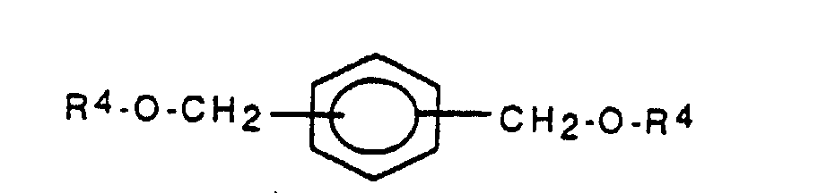
- R4
- représente un groupe CO-(OH2)n-OH3 ou un groupe CO-C6H5
où n représente un nombre entier de 0 à 5.
- Réserve selon la revendication 1, caractérisée en ce que le polymère de base est un copolymère d'anhydride maléique et de méthacrylate de glycidyle.
- Réserve selon la revendication 1, caractérisée en ce que le polymère de base est un copolymère d'anhydride maléique et du 4-(acétoxyméthyl)-styrène.
- Réserve selon la revendication 1, caractérisée en ce que le polymère de base est un terpolymère d'anhydride maléique,du 4-(acétoxyméthyl)-styrène et d'acide maléique.
- Réserve selon la revendication 1, caractérisée en ce que le polymère de base est un copolymère d'anhydride maléique et de p-méthoxystyrène.
- Réserve selon la revendication 5, caractérisée en ce qu'elle contient du p-bis-(acétoxyméthyl)-benzène à titre d'additif.
- Réserve selon l'une quelconque des revendications 1 à 6, caractérisée en ce que le composant photoactif est un sel d'onium.
- Réserve selon la revendication 7, caractérisée en ce que le composant photoactif est le trifluorométhane-sulfonate de diphényliodonium et/ou de triphénylsulfonium.
- Réserve selon une ou plusieurs des revendications 1 à 8, caractérisée en ce que le solvant est l'acétate de méthoxypropyle ou l'éther diméthylique de diéthylèneglycol.
- Utilisation de la réserve selon une ou plusieurs des revendications 1 à 9 dans la technique dans laquelle on utilise des réserves à simple recouvrement.
Applications Claiming Priority (3)
| Application Number | Priority Date | Filing Date | Title |
|---|---|---|---|
| DE4418205 | 1994-05-25 | ||
| DE4418205 | 1994-05-25 | ||
| PCT/DE1995/000626 WO1995032455A1 (fr) | 1994-05-25 | 1995-05-11 | Resist positif developpable a sec |
Publications (2)
| Publication Number | Publication Date |
|---|---|
| EP0760971A1 EP0760971A1 (fr) | 1997-03-12 |
| EP0760971B1 true EP0760971B1 (fr) | 1999-08-04 |
Family
ID=6518912
Family Applications (1)
| Application Number | Title | Priority Date | Filing Date |
|---|---|---|---|
| EP95918519A Expired - Lifetime EP0760971B1 (fr) | 1994-05-25 | 1995-05-11 | Resist positif developpable a sec |
Country Status (6)
| Country | Link |
|---|---|
| US (1) | US5733706A (fr) |
| EP (1) | EP0760971B1 (fr) |
| KR (1) | KR100382253B1 (fr) |
| CN (1) | CN1149341A (fr) |
| DE (1) | DE59506534D1 (fr) |
| WO (1) | WO1995032455A1 (fr) |
Families Citing this family (8)
| Publication number | Priority date | Publication date | Assignee | Title |
|---|---|---|---|---|
| AU3964199A (en) * | 1998-04-07 | 1999-10-25 | Euv Limited Liability Corporation | Thin layer imaging process for microlithography using radiation at strongly attenuated wavelengths |
| US6270949B1 (en) | 1998-08-11 | 2001-08-07 | International Business Machines Corporation | Single component developer for copolymer resists |
| US6426177B2 (en) | 1998-08-11 | 2002-07-30 | International Business Machines Corporation | Single component developer for use with ghost exposure |
| US6436605B1 (en) | 1999-07-12 | 2002-08-20 | International Business Machines Corporation | Plasma resistant composition and use thereof |
| US6348407B1 (en) * | 2001-03-15 | 2002-02-19 | Chartered Semiconductor Manufacturing Inc. | Method to improve adhesion of organic dielectrics in dual damascene interconnects |
| JP3999030B2 (ja) * | 2001-12-13 | 2007-10-31 | セントラル硝子株式会社 | 含フッ素重合性単量体およびそれを用いた高分子化合物、反射防止膜材料 |
| TWI335218B (en) * | 2003-02-19 | 2011-01-01 | Panion & Bf Biotech Inc | Ferric organic compounds, uses thereof and methods of making same |
| CN103035512B (zh) * | 2012-11-02 | 2015-08-19 | 上海华虹宏力半导体制造有限公司 | 一种非感光性聚酰亚胺钝化层的制作方法 |
Family Cites Families (17)
| Publication number | Priority date | Publication date | Assignee | Title |
|---|---|---|---|---|
| US4491628A (en) * | 1982-08-23 | 1985-01-01 | International Business Machines Corporation | Positive- and negative-working resist compositions with acid generating photoinitiator and polymer with acid labile groups pendant from polymer backbone |
| CA1248402A (fr) * | 1983-09-16 | 1989-01-10 | Larry E. Stillwagon | Methode de fabrication d'articles au moyen d'une couche produite par un plasma |
| US4552833A (en) * | 1984-05-14 | 1985-11-12 | International Business Machines Corporation | Radiation sensitive and oxygen plasma developable resist |
| US4551418A (en) * | 1985-02-19 | 1985-11-05 | International Business Machines Corporation | Process for preparing negative relief images with cationic photopolymerization |
| US4613398A (en) * | 1985-06-06 | 1986-09-23 | International Business Machines Corporation | Formation of etch-resistant resists through preferential permeation |
| US4657845A (en) * | 1986-01-14 | 1987-04-14 | International Business Machines Corporation | Positive tone oxygen plasma developable photoresist |
| GB8611229D0 (en) * | 1986-05-08 | 1986-06-18 | Ucb Sa | Forming positive pattern |
| NL8700421A (nl) * | 1987-02-20 | 1988-09-16 | Philips Nv | Werkwijze voor het vervaardigen van een halfgeleiderinrichting. |
| EP0307752B1 (fr) * | 1987-09-16 | 1995-02-22 | Hoechst Aktiengesellschaft | Poly(acétoxystyrènes 3-mono ou 3,5 disubstitués), et leur utilisation |
| US4921778A (en) * | 1988-07-29 | 1990-05-01 | Shipley Company Inc. | Photoresist pattern fabrication employing chemically amplified metalized material |
| US5023164A (en) * | 1989-10-23 | 1991-06-11 | International Business Machines Corporation | Highly sensitive dry developable deep UV photoresist |
| EP0451311B1 (fr) * | 1990-04-12 | 1999-03-10 | Siemens Aktiengesellschaft | Procédé pour la fabrication d'un modèle de réserve |
| DE59010396D1 (de) * | 1990-04-27 | 1996-08-01 | Siemens Ag | Verfahren zur Erzeugung einer Resiststruktur |
| EP0492256B1 (fr) * | 1990-12-20 | 1996-08-14 | Siemens Aktiengesellschaft | Création de structure par voie photolithographique |
| US5296332A (en) * | 1991-11-22 | 1994-03-22 | International Business Machines Corporation | Crosslinkable aqueous developable photoresist compositions and method for use thereof |
| US5399604A (en) * | 1992-07-24 | 1995-03-21 | Japan Synthetic Rubber Co., Ltd. | Epoxy group-containing resin compositions |
| JPH06250390A (ja) * | 1993-02-26 | 1994-09-09 | Nippon Oil & Fats Co Ltd | 光硬化性樹脂組成物 |
-
1995
- 1995-05-11 EP EP95918519A patent/EP0760971B1/fr not_active Expired - Lifetime
- 1995-05-11 KR KR1019960706662A patent/KR100382253B1/ko not_active Expired - Fee Related
- 1995-05-11 US US08/737,989 patent/US5733706A/en not_active Expired - Lifetime
- 1995-05-11 CN CN95193140A patent/CN1149341A/zh active Pending
- 1995-05-11 DE DE59506534T patent/DE59506534D1/de not_active Expired - Fee Related
- 1995-05-11 WO PCT/DE1995/000626 patent/WO1995032455A1/fr not_active Ceased
Also Published As
| Publication number | Publication date |
|---|---|
| EP0760971A1 (fr) | 1997-03-12 |
| US5733706A (en) | 1998-03-31 |
| WO1995032455A1 (fr) | 1995-11-30 |
| CN1149341A (zh) | 1997-05-07 |
| KR970703551A (ko) | 1997-07-03 |
| HK1001818A1 (en) | 1998-07-10 |
| DE59506534D1 (de) | 1999-09-09 |
| KR100382253B1 (ko) | 2003-08-21 |
Similar Documents
| Publication | Publication Date | Title |
|---|---|---|
| DE69120809T2 (de) | Positiv-resists und deren nützlichkeit in trockenresists | |
| EP0492253B1 (fr) | Procédé photolithographique | |
| DE69930832T2 (de) | Benutzung einer zusammensetzung für eine antireflexunterschicht | |
| EP0494383B1 (fr) | Photoréserve | |
| EP0492256B1 (fr) | Création de structure par voie photolithographique | |
| DE69431618T2 (de) | Strahlungsempfindliches Material und Verfahren zur Herstellung eines Musters | |
| DE60034488T2 (de) | Strahlungsempfindliche copolymere, fotoresistzusammensetzungen und zweischichtresistsysteme für den tiefen uv-bereich | |
| DE69832352T2 (de) | Verfahren zur Herstellung von Vorrichtung unter Benutzung eines strahlungsempfindlichen Resistmaterials | |
| DE19919794A1 (de) | Polymer und dessen Verwendung in einem Verfahren zur Bildung eines Mikromusters | |
| DE3817012A1 (de) | Positiv und negativ arbeitende strahlungsempfindliche gemische sowie verfahren zur herstellung von reliefmustern | |
| DE4120172A1 (de) | Strahlungsempfindliches gemisch, das als bindemittel neue polymere mit einheiten aus amiden von (alpha),(beta)-ungesaettigten carbonsaeuren enthaelt | |
| EP0957399B1 (fr) | Composition sensible aux radiations et son utilisation | |
| DE10332855A1 (de) | Verfahren zum Bilden einer Mikrostruktur auf einem Substrat unter Verwendung einer Resiststruktur, und Restistoberflächenbehandlungsmittel | |
| DE10134162A1 (de) | Neuartiges Copolymeres, Photoresistzusammensetzung und Verfahren zur Herstellung eines Photoresistmusters mit hohem Seitenverhältnis | |
| DE69120842T2 (de) | Photolackzusammensetzung und Strukturierungsmethode | |
| DE69935938T2 (de) | Ein strahlungsempfindliches Material und Verfahren zur Herstellung von einem Muster damit | |
| EP0453610B1 (fr) | Procédé pour réaliser des structures de réserve | |
| WO1995032455A1 (fr) | Resist positif developpable a sec | |
| EP0874281A1 (fr) | Réserve chimiquement amplifiée | |
| EP0797792B1 (fr) | Production de structures par photolithographie | |
| EP0451311B1 (fr) | Procédé pour la fabrication d'un modèle de réserve | |
| EP0781424B1 (fr) | Production de structures par photolithographie | |
| US5328973A (en) | Radiation-sensitive mixture with a polymeric binder containing units of α,β-unsaturated carboxamides | |
| EP0388484B1 (fr) | Photoréserve à haute résolution | |
| DE4226464B4 (de) | Positivresist |
Legal Events
| Date | Code | Title | Description |
|---|---|---|---|
| PUAI | Public reference made under article 153(3) epc to a published international application that has entered the european phase |
Free format text: ORIGINAL CODE: 0009012 |
|
| 17P | Request for examination filed |
Effective date: 19961022 |
|
| AK | Designated contracting states |
Kind code of ref document: A1 Designated state(s): BE CH DE FR GB LI NL SE |
|
| GRAG | Despatch of communication of intention to grant |
Free format text: ORIGINAL CODE: EPIDOS AGRA |
|
| 17Q | First examination report despatched |
Effective date: 19980819 |
|
| GRAG | Despatch of communication of intention to grant |
Free format text: ORIGINAL CODE: EPIDOS AGRA |
|
| GRAH | Despatch of communication of intention to grant a patent |
Free format text: ORIGINAL CODE: EPIDOS IGRA |
|
| GRAH | Despatch of communication of intention to grant a patent |
Free format text: ORIGINAL CODE: EPIDOS IGRA |
|
| GRAH | Despatch of communication of intention to grant a patent |
Free format text: ORIGINAL CODE: EPIDOS IGRA |
|
| GRAA | (expected) grant |
Free format text: ORIGINAL CODE: 0009210 |
|
| AK | Designated contracting states |
Kind code of ref document: B1 Designated state(s): BE CH DE FR GB LI NL SE |
|
| REG | Reference to a national code |
Ref country code: CH Ref legal event code: NV Representative=s name: SIEMENS SCHWEIZ AG Ref country code: CH Ref legal event code: EP |
|
| REF | Corresponds to: |
Ref document number: 59506534 Country of ref document: DE Date of ref document: 19990909 |
|
| ET | Fr: translation filed | ||
| PLBE | No opposition filed within time limit |
Free format text: ORIGINAL CODE: 0009261 |
|
| STAA | Information on the status of an ep patent application or granted ep patent |
Free format text: STATUS: NO OPPOSITION FILED WITHIN TIME LIMIT |
|
| 26N | No opposition filed | ||
| REG | Reference to a national code |
Ref country code: GB Ref legal event code: IF02 |
|
| PGFP | Annual fee paid to national office [announced via postgrant information from national office to epo] |
Ref country code: CH Payment date: 20060515 Year of fee payment: 12 |
|
| REG | Reference to a national code |
Ref country code: CH Ref legal event code: PL |
|
| PG25 | Lapsed in a contracting state [announced via postgrant information from national office to epo] |
Ref country code: LI Free format text: LAPSE BECAUSE OF NON-PAYMENT OF DUE FEES Effective date: 20070531 Ref country code: CH Free format text: LAPSE BECAUSE OF NON-PAYMENT OF DUE FEES Effective date: 20070531 |
|
| PGFP | Annual fee paid to national office [announced via postgrant information from national office to epo] |
Ref country code: BE Payment date: 20080620 Year of fee payment: 14 |
|
| PGFP | Annual fee paid to national office [announced via postgrant information from national office to epo] |
Ref country code: SE Payment date: 20080513 Year of fee payment: 14 Ref country code: NL Payment date: 20080515 Year of fee payment: 14 Ref country code: DE Payment date: 20080715 Year of fee payment: 14 |
|
| PGFP | Annual fee paid to national office [announced via postgrant information from national office to epo] |
Ref country code: GB Payment date: 20080522 Year of fee payment: 14 |
|
| BERE | Be: lapsed |
Owner name: *SIEMENS A.G. Effective date: 20090531 |
|
| GBPC | Gb: european patent ceased through non-payment of renewal fee |
Effective date: 20090511 |
|
| NLV4 | Nl: lapsed or anulled due to non-payment of the annual fee |
Effective date: 20091201 |
|
| PG25 | Lapsed in a contracting state [announced via postgrant information from national office to epo] |
Ref country code: NL Free format text: LAPSE BECAUSE OF NON-PAYMENT OF DUE FEES Effective date: 20091201 |
|
| REG | Reference to a national code |
Ref country code: FR Ref legal event code: ST Effective date: 20100129 |
|
| PG25 | Lapsed in a contracting state [announced via postgrant information from national office to epo] |
Ref country code: FR Free format text: LAPSE BECAUSE OF NON-PAYMENT OF DUE FEES Effective date: 20090602 |
|
| PGFP | Annual fee paid to national office [announced via postgrant information from national office to epo] |
Ref country code: FR Payment date: 20080425 Year of fee payment: 14 |
|
| PG25 | Lapsed in a contracting state [announced via postgrant information from national office to epo] |
Ref country code: GB Free format text: LAPSE BECAUSE OF NON-PAYMENT OF DUE FEES Effective date: 20090511 |
|
| PG25 | Lapsed in a contracting state [announced via postgrant information from national office to epo] |
Ref country code: DE Free format text: LAPSE BECAUSE OF NON-PAYMENT OF DUE FEES Effective date: 20091201 Ref country code: BE Free format text: LAPSE BECAUSE OF NON-PAYMENT OF DUE FEES Effective date: 20090531 |
|
| PG25 | Lapsed in a contracting state [announced via postgrant information from national office to epo] |
Ref country code: SE Free format text: LAPSE BECAUSE OF NON-PAYMENT OF DUE FEES Effective date: 20090512 |