EP0762073A1 - Halbleiterzündungsvorrichtung und Verfahren zum Bilden einer solchen Vorrichtung - Google Patents
Halbleiterzündungsvorrichtung und Verfahren zum Bilden einer solchen Vorrichtung Download PDFInfo
- Publication number
- EP0762073A1 EP0762073A1 EP96112874A EP96112874A EP0762073A1 EP 0762073 A1 EP0762073 A1 EP 0762073A1 EP 96112874 A EP96112874 A EP 96112874A EP 96112874 A EP96112874 A EP 96112874A EP 0762073 A1 EP0762073 A1 EP 0762073A1
- Authority
- EP
- European Patent Office
- Prior art keywords
- active layer
- semiconductor
- forming
- layer
- fuse
- Prior art date
- Legal status (The legal status is an assumption and is not a legal conclusion. Google has not performed a legal analysis and makes no representation as to the accuracy of the status listed.)
- Granted
Links
Images

Classifications
-
- H—ELECTRICITY
- H10—SEMICONDUCTOR DEVICES; ELECTRIC SOLID-STATE DEVICES NOT OTHERWISE PROVIDED FOR
- H10W—GENERIC PACKAGES, INTERCONNECTIONS, CONNECTORS OR OTHER CONSTRUCTIONAL DETAILS OF DEVICES COVERED BY CLASS H10
- H10W20/00—Interconnections in chips, wafers or substrates
- H10W20/40—Interconnections external to wafers or substrates, e.g. back-end-of-line [BEOL] metallisations or vias connecting to gate electrodes
- H10W20/49—Adaptable interconnections, e.g. fuses or antifuses
- H10W20/493—Fuses, i.e. interconnections changeable from conductive to non-conductive
-
- F—MECHANICAL ENGINEERING; LIGHTING; HEATING; WEAPONS; BLASTING
- F42—AMMUNITION; BLASTING
- F42B—EXPLOSIVE CHARGES, e.g. FOR BLASTING, FIREWORKS, AMMUNITION
- F42B3/00—Blasting cartridges, i.e. case and explosive
- F42B3/10—Initiators therefor
- F42B3/12—Bridge initiators
- F42B3/13—Bridge initiators with semiconductive bridge
Definitions
- This invention relates to a semiconductor fuse device for an igniter device and a method for forming a semiconductor fuse device for an igniter device.
- igniters for igniting explosive materials in, for example, mining applications and also to blow up air bags or retract seat belts in automobiles for passenger safety.
- Igniters typically comprise a fuse device having a fuse element which is located in proximity to the explosive material such that when the fuse element is energised, the explosive material is ignited.
- the fuse element may be a wire which passes through a cavity containing the explosive material and which is energised by passing a firing current through the wire.
- German patent application no. GB-A-2190730 and US patent no. US-A-4,708,060 disclose igniters having a semiconductor fuse device.
- Such semiconductor fuse devices generally comprise a fuse element positioned on a substrate between two contacts.
- External control circuitry is coupled to the two contacts via, for example, wire contacts and provides the firing current at the appropriate time which heats the fuse element and ignites the explosive material.
- the fuse element is formed, for example, from a conductive metal layer formed on the substrate or from a polysilicon layer formed on an oxide layer, such as silicon dioxide, formed on the substrate or from a doped silicon layer formed on the substrate.
- the operation of a semiconductor fuse device is dependent on the level of the firing current required to ignite the explosive material, the resistance of the fuse element, the level of the "no-fire” current and the ability of the device to withstand electrostatic discharge (ESD) and electromagnetic interference (EMI).
- ESD electrostatic discharge
- EMI electromagnetic interference
- a method for forming a semiconductor fuse device having a fuse element for an igniter device comprising the steps of:
- the method in accordance with the present invention thus provides an active layer that is sufficiently deep to ensure that the firing current is reduced, whilst not degrading the ESD and EMI response of the device nor varying the fuse resistance.
- An advantage of the invention is that it avoids the need for additional process steps as required by the prior art multi-layered structures.
- the step of forming a single active layer on the insulator layer comprises the step of atomic bonding an active layer to the insulator layer.
- the forming an active layer step may include an additional step of patterning and etching at least one trench in a surface of the active layer before the step of atomic bonding the surface of the active layer to the insulator layer.
- the steps of forming an insulator layer and a single active layer on the insulator layer comprise the step of bombarding the substrate with high energy oxygen so as to form an oxide insulator layer between two portions of the substrate, the active layer being formed by one of the two portions of the substrate.
- the predetermined depth of the active layer is 10 microns.
- Circuitry for controlling the operation of the semiconductor fuse device may be integrated into the active layer by forming isolation trenches in the active layer to provide an active device region isolated from the fuse element and integrating the circuitry into the active device region.
- a semiconductor fuse device and a semiconductor igniter device comprising a semiconductor fuse device with integrated circuitry are also disclosed and claimed.
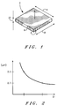
- the main operating parameters of a semiconductor fuse device include the level of the firing current (If), the ability to withstand ESD and EMI, and fuse resistance.
- ESD is a function of the width 4 of the fuse element
- the resistance is a function of cross-sectional area A and width 4
- the level of the firing current is an inverse function (see FIG. 2) of the area 6 of the fuse element which is in contact with the explosive material (not shown).
- the inventors have realised that a reduction in power consumption can be obtained, whilst maintaining the same resistance value and not degrading the ESD, by increasing the depth 10 and reducing the length 8 of the fuse element.
- the present invention provides the required ESD standard, reduced level of firing current and maintained fuse resistance without the above mentioned disadvantages.
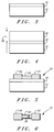
- a first method for forming a semiconductor fuse device in accordance with a first embodiment of the present invention will now be described with reference to FIGs. 3 to 6.
- the first embodiment uses the technique of atomic or wafer bonding.
- a substrate 12 is provided and an insulator layer 14 is formed on the substrate (FIG. 3).
- the insulator layer 14 may be formed of any material which provides a barrier to the transfer of heat, such as an oxide layer or nitride layer.
- a silicon dioxide layer is formed on a silicon wafer having a minimum depth of 0.5 microns.
- An active layer 16 is then atomically bonded to the insulator layer 14 (FIG. 4).
- Atomic bonding processes are well known in the art. The following method is an example of how the active layer 16 can be atomically bonded to the insulator layer 14.
- the insulator layer 14 and active layer 16 are cleaned with the following sequence: firstly, organic removal, followed by native oxide etching in diluted hydrofluoric acid solution (HF), then a water rinse and finally drying in warm nitrogen.
- HF diluted hydrofluoric acid solution
- the two hydrophobic surfaces of the insulator layer 14 and active layer 16 are immediately contacted together in a class 10 clean room with a flats misorientation between ⁇ 2°.
- two layers 14, 16 of different orientations can be bonded together. While the two layers 14, 16 are in contact at room temperature, the two layers are pre-strained in order to make the contact begin at the centre of the layers so as to avoid voids during a following heat treatment step. The value of the strain should be controlled and not too high.
- the heat treatment step is performed in nitrogen ambient at 1200°C for approximately 50 minutes in order to bond the layers.
- the exposed surface of the active layer is ground to the required or predetermined depth 18. The surface is then polished.
- the depth of the active layer 16 is greater than 4 microns. Preferably, it is within the range of 10 to 15 microns. However, the preferred depth is 10 microns since this meets the requirements of reduced firing current, maintained fuse resistance and ESD whilst providing good reproducibility.
- the active layer 16 is then patterned and etch to form the fuse element 20 having a predetermined depth 18 and length 26.
- Contacts 22 and 24 are formed in conventional manner.
- FIGs. 5 and 6 show the semiconductor fuse device 23.
- the active layer 16 may be formed from any conductive material which forms atomic bonds with the insulator layer 14.
- a silicon active layer 16 is bonded to a silicon dioxide insulator layer 14.
- the active layer 16 may also be silicon doped with arsenic or phosphorus or antimony or arsenic.
- the substrate and active layer can be formed of a material having any conductivity type, that is, N + , N - , P + , P - .
- the above described method in accordance with the present invention may include an additional step of patterning and etching at least one trench 17 in the surface of the active layer 16 before bonding the surface to the insulator layer 14 (see FIG. 7). As described above, after bonding the active layer 16 is then ground and polished to achieve the desired depth 18 of active layer 16 (see FIG. 8).
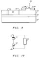
- the method in accordance with the first embodiment of the present invention can be used to form an igniter device arrangement shown in FIG. 9.
- Like components are referred to by the same reference numeral multiplied by 10.
- the active layer 16 can be patterned and etched as shown in FIG. 9 to form the fuse element 200. Isolation trenches 280 and 300 can then be formed in the active layer 16 so as to provide an active device region 302 isolated from the semiconductor fuse device 201 such that circuitry can be integrated into the active device region.
- the circuitry may include zener diodes, such as the two back-to-back zener diodes 402 and 404 shown in FIG. 10, to provide enhanced ESD protection.
- the two zener diodes 402 and 404 are coupled across the semiconductor fuse element 400 between two contacts 406 and 408.
- the circuitry may also include more complex combinations of active elements to control the operation of the semiconductor fuse device. Such an arrangement would avoid the need for external circuitry.
- the present invention has so far been described with reference to atomic or wafer bonding an active layer to an insulator layer on a substrate so as to provide an active layer having a depth greater than 4 microns. It is not intended that the invention be limited to atomic bonding only. Other methods such as high energy oxygen implant may be used.
- a substrate such as a silicon substrate
- high energy oxygen such that the oxygen migrates through the substrate to form an oxide insulator layer 514 as shown in FIG. 11.
- Circuitry may be integrated into the active layer as described above.
- a method for forming a semiconductor fuse device in accordance with the present invention provides an active layer that is sufficiently deep to ensure that the firing current is reduced, the ESD is not degraded and the fuse resistance is not varied, but without the need for multi-layer structures and their associated additional process steps as required by the prior art processes.
- a further advantage of the method in accordance with the present invention is that it allows integration of simple or complex functions.
- the single active layer having a depth greater than 4 microns means that circuitry, such as zener diodes to enhance ESD protection and more complex control circuitry to control the operation of the semiconductor fuse device can be integrated into the active layer.
- the substrate and active layer can be formed of a material having any conductivity type, that is, N + , N - , P + , P - , the present invention allows greater flexibility for integrating functions with the semiconductor fuse device.
Landscapes
- Engineering & Computer Science (AREA)
- General Engineering & Computer Science (AREA)
- Design And Manufacture Of Integrated Circuits (AREA)
- Semiconductor Integrated Circuits (AREA)
- Fuses (AREA)
Applications Claiming Priority (2)
| Application Number | Priority Date | Filing Date | Title |
|---|---|---|---|
| FR9510374 | 1995-09-05 | ||
| FR9510374A FR2738334A1 (fr) | 1995-09-05 | 1995-09-05 | Dispositif allumeur a semiconducteur, pour declenchement pyrotechnique, et procede de formation d'un tel dispositif |
Publications (2)
| Publication Number | Publication Date |
|---|---|
| EP0762073A1 true EP0762073A1 (de) | 1997-03-12 |
| EP0762073B1 EP0762073B1 (de) | 2001-11-28 |
Family
ID=9482270
Family Applications (1)
| Application Number | Title | Priority Date | Filing Date |
|---|---|---|---|
| EP96112874A Expired - Lifetime EP0762073B1 (de) | 1995-09-05 | 1996-08-09 | Halbleiterzündungsvorrichtung und Verfahren zum Bilden einer solchen Vorrichtung |
Country Status (6)
| Country | Link |
|---|---|
| US (1) | US5798475A (de) |
| EP (1) | EP0762073B1 (de) |
| JP (1) | JPH09115416A (de) |
| KR (1) | KR970018419A (de) |
| DE (1) | DE69617341T2 (de) |
| FR (1) | FR2738334A1 (de) |
Cited By (5)
| Publication number | Priority date | Publication date | Assignee | Title |
|---|---|---|---|---|
| WO1998054535A1 (de) * | 1997-05-26 | 1998-12-03 | Temic Telefunken Microelectronic Gmbh | Dünnschichtanzündelement für pyrotechnische wirkmassen und verfahren zu dessen herstellung |
| WO1999042784A1 (de) * | 1998-02-19 | 1999-08-26 | Robert Bosch Gmbh | Zündvorrichtung für einen gasgenerator einer rückhalteeinrichtung |
| EP0949479A1 (de) | 1998-04-09 | 1999-10-13 | DaimlerChrysler AG | Halbleiterzünder |
| FR2784176A1 (fr) * | 1998-10-06 | 2000-04-07 | Livbag Snc | Systeme d'initiation electro-pyrotechnique protege contre les decharges electrostatiques |
| WO2008112235A1 (en) * | 2007-03-12 | 2008-09-18 | Dyno Nobel Inc. | Detonator ignition protection circuit |
Families Citing this family (13)
| Publication number | Priority date | Publication date | Assignee | Title |
|---|---|---|---|---|
| JPH08222710A (ja) | 1995-02-17 | 1996-08-30 | Mitsubishi Electric Corp | 半導体装置 |
| US5847309A (en) * | 1995-08-24 | 1998-12-08 | Auburn University | Radio frequency and electrostatic discharge insensitive electro-explosive devices having non-linear resistances |
| US6199484B1 (en) * | 1997-01-06 | 2001-03-13 | The Ensign-Bickford Company | Voltage-protected semiconductor bridge igniter elements |
| US5992326A (en) * | 1997-01-06 | 1999-11-30 | The Ensign-Bickford Company | Voltage-protected semiconductor bridge igniter elements |
| DE19756603C1 (de) * | 1997-12-18 | 1999-06-24 | Siemens Ag | Integrierte Schaltungsanordnung mit einem Kondensator und einem Zündelement sowie Verwendung einer solchen Schaltungsanordnung |
| DE10006528C2 (de) * | 2000-02-15 | 2001-12-06 | Infineon Technologies Ag | Fuseanordnung für eine Halbleitervorrichtung |
| US6772692B2 (en) * | 2000-05-24 | 2004-08-10 | Lifesparc, Inc. | Electro-explosive device with laminate bridge |
| EP1421328A4 (de) * | 2001-08-28 | 2008-10-01 | Ensign Bickford Aerospace & De | Röhrenförmige zünderbrücke |
| US6774457B2 (en) * | 2001-09-13 | 2004-08-10 | Texas Instruments Incorporated | Rectangular contact used as a low voltage fuse element |
| US20050132919A1 (en) * | 2003-12-17 | 2005-06-23 | Honda Motor Co., Ltd. | Squib |
| KR100534102B1 (ko) * | 2004-04-21 | 2005-12-06 | 삼성전자주식회사 | 반도체 기억소자의 퓨즈 영역들 및 그 제조방법들 |
| WO2015060278A1 (ja) * | 2013-10-24 | 2015-04-30 | 株式会社村田製作所 | 複合保護回路、複合保護素子および照明用led素子 |
| WO2023095535A1 (ja) * | 2021-11-26 | 2023-06-01 | 株式会社オートネットワーク技術研究所 | 遮断装置 |
Citations (6)
| Publication number | Priority date | Publication date | Assignee | Title |
|---|---|---|---|---|
| GB2006402A (en) * | 1977-10-20 | 1979-05-02 | Dynamit Nobel Ag | Electric firing element |
| US4708060A (en) | 1985-02-19 | 1987-11-24 | The United States Of America As Represented By The United States Department Of Energy | Semiconductor bridge (SCB) igniter |
| GB2190730A (en) | 1986-05-22 | 1987-11-25 | Detonix Close Corp | Detonator firing element |
| US4855804A (en) * | 1987-11-17 | 1989-08-08 | Motorola, Inc. | Multilayer trench isolation process and structure |
| US5094167A (en) * | 1990-03-14 | 1992-03-10 | Schlumberger Technology Corporation | Shape charge for a perforating gun including an integrated circuit detonator and wire contactor responsive to ordinary current for detonation |
| US5372673A (en) * | 1993-01-25 | 1994-12-13 | Motorola, Inc. | Method for processing a layer of material while using insitu monitoring and control |
Family Cites Families (9)
| Publication number | Priority date | Publication date | Assignee | Title |
|---|---|---|---|---|
| US4843964A (en) * | 1988-02-01 | 1989-07-04 | The United States Of America As Represented By The United States Department Of Energy | Smart explosive igniter |
| US4937094A (en) * | 1988-05-26 | 1990-06-26 | Energy Conversion Devices, Inc. | Method of creating a high flux of activated species for reaction with a remotely located substrate |
| US4976200A (en) * | 1988-12-30 | 1990-12-11 | The United States Of America As Represented By The United States Department Of Energy | Tungsten bridge for the low energy ignition of explosive and energetic materials |
| US4967665A (en) * | 1989-07-24 | 1990-11-06 | The United States Of America As Represented By The Secretary Of The Navy | RF and DC desensitized electroexplosive device |
| US5088329A (en) * | 1990-05-07 | 1992-02-18 | Sahagen Armen N | Piezoresistive pressure transducer |
| US5085146A (en) * | 1990-05-17 | 1992-02-04 | Auburn University | Electroexplosive device |
| US5309841A (en) * | 1991-10-08 | 1994-05-10 | Scb Technologies, Inc. | Zener diode for protection of integrated circuit explosive bridge |
| US5371378A (en) * | 1992-06-08 | 1994-12-06 | Kobe Steel Usa, Inc. | Diamond metal base/permeable base transistor and method of making same |
| WO1995026571A1 (en) * | 1994-03-25 | 1995-10-05 | Amoco/Enron Solar | Stabilized amorphous silicon and devices containing same |
-
1995
- 1995-09-05 FR FR9510374A patent/FR2738334A1/fr active Pending
-
1996
- 1996-07-29 US US08/681,780 patent/US5798475A/en not_active Expired - Fee Related
- 1996-08-09 DE DE69617341T patent/DE69617341T2/de not_active Expired - Fee Related
- 1996-08-09 EP EP96112874A patent/EP0762073B1/de not_active Expired - Lifetime
- 1996-08-29 JP JP8247214A patent/JPH09115416A/ja active Pending
- 1996-09-04 KR KR1019960038170A patent/KR970018419A/ko not_active Abandoned
Patent Citations (6)
| Publication number | Priority date | Publication date | Assignee | Title |
|---|---|---|---|---|
| GB2006402A (en) * | 1977-10-20 | 1979-05-02 | Dynamit Nobel Ag | Electric firing element |
| US4708060A (en) | 1985-02-19 | 1987-11-24 | The United States Of America As Represented By The United States Department Of Energy | Semiconductor bridge (SCB) igniter |
| GB2190730A (en) | 1986-05-22 | 1987-11-25 | Detonix Close Corp | Detonator firing element |
| US4855804A (en) * | 1987-11-17 | 1989-08-08 | Motorola, Inc. | Multilayer trench isolation process and structure |
| US5094167A (en) * | 1990-03-14 | 1992-03-10 | Schlumberger Technology Corporation | Shape charge for a perforating gun including an integrated circuit detonator and wire contactor responsive to ordinary current for detonation |
| US5372673A (en) * | 1993-01-25 | 1994-12-13 | Motorola, Inc. | Method for processing a layer of material while using insitu monitoring and control |
Cited By (12)
| Publication number | Priority date | Publication date | Assignee | Title |
|---|---|---|---|---|
| WO1998054535A1 (de) * | 1997-05-26 | 1998-12-03 | Temic Telefunken Microelectronic Gmbh | Dünnschichtanzündelement für pyrotechnische wirkmassen und verfahren zu dessen herstellung |
| WO1999042784A1 (de) * | 1998-02-19 | 1999-08-26 | Robert Bosch Gmbh | Zündvorrichtung für einen gasgenerator einer rückhalteeinrichtung |
| EP0949479A1 (de) | 1998-04-09 | 1999-10-13 | DaimlerChrysler AG | Halbleiterzünder |
| DE19815928A1 (de) * | 1998-04-09 | 1999-11-04 | Daimler Chrysler Ag | Halbleiterzünder mit verbesserter konstruktiver Festigkeit |
| DE19815928C2 (de) * | 1998-04-09 | 2000-05-11 | Daimler Chrysler Ag | Halbleiterzünder mit verbesserter konstruktiver Festigkeit |
| US6220164B1 (en) | 1998-04-09 | 2001-04-24 | Daimlerchrysler Ag | Semiconductor igniter |
| FR2784176A1 (fr) * | 1998-10-06 | 2000-04-07 | Livbag Snc | Systeme d'initiation electro-pyrotechnique protege contre les decharges electrostatiques |
| EP0992760A1 (de) * | 1998-10-06 | 2000-04-12 | Livbag S.N.C. | Gegen elektrostatische Entladungen geschütztes elektro-pyrotechnisches Zündsystem |
| US6220163B1 (en) | 1998-10-06 | 2001-04-24 | Livbag Snc | Electro-pyrotechnic initiation system protected against electrostatic discharges |
| WO2008112235A1 (en) * | 2007-03-12 | 2008-09-18 | Dyno Nobel Inc. | Detonator ignition protection circuit |
| US8166879B2 (en) | 2007-03-12 | 2012-05-01 | Dyno Nobel Inc. | Detonator ignition protection circuit |
| CN101680734B (zh) * | 2007-03-12 | 2014-04-09 | 戴诺·诺贝尔公司 | 引爆器点火保护电路 |
Also Published As
| Publication number | Publication date |
|---|---|
| JPH09115416A (ja) | 1997-05-02 |
| US5798475A (en) | 1998-08-25 |
| EP0762073B1 (de) | 2001-11-28 |
| DE69617341D1 (de) | 2002-01-10 |
| FR2738334A1 (fr) | 1997-03-07 |
| DE69617341T2 (de) | 2002-07-25 |
| KR970018419A (ko) | 1997-04-30 |
Similar Documents
| Publication | Publication Date | Title |
|---|---|---|
| EP0762073B1 (de) | Halbleiterzündungsvorrichtung und Verfahren zum Bilden einer solchen Vorrichtung | |
| US6346459B1 (en) | Process for lift off and transfer of semiconductor devices onto an alien substrate | |
| EP1979949B1 (de) | Halbleiterstruktur mit einem grabenkondensator und einem grabenwiderstand | |
| US5286670A (en) | Method of manufacturing a semiconductor device having buried elements with electrical characteristic | |
| US5304506A (en) | On chip decoupling capacitor | |
| KR100358629B1 (ko) | 반도체 디바이스 구조물 | |
| US5763299A (en) | Reduced leakage antifuse fabrication method | |
| EP1351304B1 (de) | Kondensatoren für integrierten Schaltkreis | |
| EP0130412B1 (de) | Halbleitervorrichtung mit einer Schutzschaltung | |
| JPS60226163A (ja) | シヨツトキ−バイポ−ラトランジスタを有するcmos構造を製造する方法 | |
| EP0739037A3 (de) | Halbleiterbauelement mit Kondensator und dessen Herstellungsverfahren | |
| US5841182A (en) | Capacitor structure in a bonded wafer and method of fabrication | |
| US6524898B2 (en) | Method of fabricating a protective element in an SOI substrate | |
| US6507103B2 (en) | Semiconductor device | |
| JPH02502417A (ja) | 半導体素子の製造方法 | |
| KR100829404B1 (ko) | 모놀리식으로 형성된 저항기-커패시터 부분을 갖는 정전기방전 보호 장치 | |
| JPH11260909A (ja) | デカップリング・キャパシタンスを有する半導体デバイスおよびその製造方法 | |
| US5892292A (en) | Getterer for multi-layer wafers and method for making same | |
| KR20010024742A (ko) | 이그니션 물질을 가열하기 위한 집적 회로 장치와 그러한집적 회로 장치의 사용방법 | |
| EP0697708B1 (de) | Halbleitersicherungsanordnung | |
| US5843835A (en) | Damage free gate dielectric process during gate electrode plasma etching | |
| CN111446365B (zh) | 一种隔离电容器和用于形成隔离电容的方法 | |
| ZA200702946B (en) | Detonator device | |
| US20010045610A1 (en) | Micro-machined surface structure | |
| US20040261645A1 (en) | Tubular igniter bridge |
Legal Events
| Date | Code | Title | Description |
|---|---|---|---|
| PUAI | Public reference made under article 153(3) epc to a published international application that has entered the european phase |
Free format text: ORIGINAL CODE: 0009012 |
|
| AK | Designated contracting states |
Kind code of ref document: A1 Designated state(s): DE |
|
| 17P | Request for examination filed |
Effective date: 19970912 |
|
| 17Q | First examination report despatched |
Effective date: 19990303 |
|
| GRAG | Despatch of communication of intention to grant |
Free format text: ORIGINAL CODE: EPIDOS AGRA |
|
| GRAG | Despatch of communication of intention to grant |
Free format text: ORIGINAL CODE: EPIDOS AGRA |
|
| GRAH | Despatch of communication of intention to grant a patent |
Free format text: ORIGINAL CODE: EPIDOS IGRA |
|
| GRAH | Despatch of communication of intention to grant a patent |
Free format text: ORIGINAL CODE: EPIDOS IGRA |
|
| GRAA | (expected) grant |
Free format text: ORIGINAL CODE: 0009210 |
|
| AK | Designated contracting states |
Kind code of ref document: B1 Designated state(s): DE |
|
| REF | Corresponds to: |
Ref document number: 69617341 Country of ref document: DE Date of ref document: 20020110 |
|
| PLBE | No opposition filed within time limit |
Free format text: ORIGINAL CODE: 0009261 |
|
| STAA | Information on the status of an ep patent application or granted ep patent |
Free format text: STATUS: NO OPPOSITION FILED WITHIN TIME LIMIT |
|
| 26N | No opposition filed | ||
| PGFP | Annual fee paid to national office [announced via postgrant information from national office to epo] |
Ref country code: DE Payment date: 20060831 Year of fee payment: 11 |
|
| PG25 | Lapsed in a contracting state [announced via postgrant information from national office to epo] |
Ref country code: DE Free format text: LAPSE BECAUSE OF NON-PAYMENT OF DUE FEES Effective date: 20080301 |