EP0762216A2 - Belichtungsverfahren und -vorrichtung und Verfahren und Vorrichtung zur Bewertung einer Ausrichtung - Google Patents
Belichtungsverfahren und -vorrichtung und Verfahren und Vorrichtung zur Bewertung einer Ausrichtung Download PDFInfo
- Publication number
- EP0762216A2 EP0762216A2 EP96306266A EP96306266A EP0762216A2 EP 0762216 A2 EP0762216 A2 EP 0762216A2 EP 96306266 A EP96306266 A EP 96306266A EP 96306266 A EP96306266 A EP 96306266A EP 0762216 A2 EP0762216 A2 EP 0762216A2
- Authority
- EP
- European Patent Office
- Prior art keywords
- exposure
- discrimination
- positioning
- accordance
- deviation
- Prior art date
- Legal status (The legal status is an assumption and is not a legal conclusion. Google has not performed a legal analysis and makes no representation as to the accuracy of the status listed.)
- Granted
Links
Images



Classifications
-
- G—PHYSICS
- G03—PHOTOGRAPHY; CINEMATOGRAPHY; ANALOGOUS TECHNIQUES USING WAVES OTHER THAN OPTICAL WAVES; ELECTROGRAPHY; HOLOGRAPHY
- G03F—PHOTOMECHANICAL PRODUCTION OF TEXTURED OR PATTERNED SURFACES, e.g. FOR PRINTING, FOR PROCESSING OF SEMICONDUCTOR DEVICES; MATERIALS THEREFOR; ORIGINALS THEREFOR; APPARATUS SPECIALLY ADAPTED THEREFOR
- G03F7/00—Photomechanical, e.g. photolithographic, production of textured or patterned surfaces, e.g. printing surfaces; Materials therefor, e.g. comprising photoresists; Apparatus specially adapted therefor
- G03F7/70—Microphotolithographic exposure; Apparatus therefor
- G03F7/70483—Information management; Active and passive control; Testing; Wafer monitoring, e.g. pattern monitoring
- G03F7/70605—Workpiece metrology
- G03F7/70616—Monitoring the printed patterns
- G03F7/70633—Overlay, i.e. relative alignment between patterns printed by separate exposures in different layers, or in the same layer in multiple exposures or stitching
-
- H—ELECTRICITY
- H10—SEMICONDUCTOR DEVICES; ELECTRIC SOLID-STATE DEVICES NOT OTHERWISE PROVIDED FOR
- H10P—GENERIC PROCESSES OR APPARATUS FOR THE MANUFACTURE OR TREATMENT OF DEVICES COVERED BY CLASS H10
- H10P76/00—Manufacture or treatment of masks on semiconductor bodies, e.g. by lithography or photolithography
-
- G—PHYSICS
- G03—PHOTOGRAPHY; CINEMATOGRAPHY; ANALOGOUS TECHNIQUES USING WAVES OTHER THAN OPTICAL WAVES; ELECTROGRAPHY; HOLOGRAPHY
- G03F—PHOTOMECHANICAL PRODUCTION OF TEXTURED OR PATTERNED SURFACES, e.g. FOR PRINTING, FOR PROCESSING OF SEMICONDUCTOR DEVICES; MATERIALS THEREFOR; ORIGINALS THEREFOR; APPARATUS SPECIALLY ADAPTED THEREFOR
- G03F7/00—Photomechanical, e.g. photolithographic, production of textured or patterned surfaces, e.g. printing surfaces; Materials therefor, e.g. comprising photoresists; Apparatus specially adapted therefor
- G03F7/70—Microphotolithographic exposure; Apparatus therefor
- G03F7/70216—Mask projection systems
- G03F7/70358—Scanning exposure, i.e. relative movement of patterned beam and workpiece during imaging
-
- G—PHYSICS
- G03—PHOTOGRAPHY; CINEMATOGRAPHY; ANALOGOUS TECHNIQUES USING WAVES OTHER THAN OPTICAL WAVES; ELECTROGRAPHY; HOLOGRAPHY
- G03F—PHOTOMECHANICAL PRODUCTION OF TEXTURED OR PATTERNED SURFACES, e.g. FOR PRINTING, FOR PROCESSING OF SEMICONDUCTOR DEVICES; MATERIALS THEREFOR; ORIGINALS THEREFOR; APPARATUS SPECIALLY ADAPTED THEREFOR
- G03F7/00—Photomechanical, e.g. photolithographic, production of textured or patterned surfaces, e.g. printing surfaces; Materials therefor, e.g. comprising photoresists; Apparatus specially adapted therefor
- G03F7/70—Microphotolithographic exposure; Apparatus therefor
- G03F7/70425—Imaging strategies, e.g. for increasing throughput or resolution, printing product fields larger than the image field or compensating lithography- or non-lithography errors, e.g. proximity correction, mix-and-match, stitching or double patterning
-
- G—PHYSICS
- G03—PHOTOGRAPHY; CINEMATOGRAPHY; ANALOGOUS TECHNIQUES USING WAVES OTHER THAN OPTICAL WAVES; ELECTROGRAPHY; HOLOGRAPHY
- G03F—PHOTOMECHANICAL PRODUCTION OF TEXTURED OR PATTERNED SURFACES, e.g. FOR PRINTING, FOR PROCESSING OF SEMICONDUCTOR DEVICES; MATERIALS THEREFOR; ORIGINALS THEREFOR; APPARATUS SPECIALLY ADAPTED THEREFOR
- G03F7/00—Photomechanical, e.g. photolithographic, production of textured or patterned surfaces, e.g. printing surfaces; Materials therefor, e.g. comprising photoresists; Apparatus specially adapted therefor
- G03F7/70—Microphotolithographic exposure; Apparatus therefor
- G03F7/70691—Handling of masks or workpieces
- G03F7/70716—Stages
- G03F7/70725—Stages control
-
- G—PHYSICS
- G03—PHOTOGRAPHY; CINEMATOGRAPHY; ANALOGOUS TECHNIQUES USING WAVES OTHER THAN OPTICAL WAVES; ELECTROGRAPHY; HOLOGRAPHY
- G03F—PHOTOMECHANICAL PRODUCTION OF TEXTURED OR PATTERNED SURFACES, e.g. FOR PRINTING, FOR PROCESSING OF SEMICONDUCTOR DEVICES; MATERIALS THEREFOR; ORIGINALS THEREFOR; APPARATUS SPECIALLY ADAPTED THEREFOR
- G03F7/00—Photomechanical, e.g. photolithographic, production of textured or patterned surfaces, e.g. printing surfaces; Materials therefor, e.g. comprising photoresists; Apparatus specially adapted therefor
- G03F7/70—Microphotolithographic exposure; Apparatus therefor
- G03F7/708—Construction of apparatus, e.g. environment aspects, hygiene aspects or materials
- G03F7/70858—Environment aspects, e.g. pressure of beam-path gas, temperature
- G03F7/709—Vibration, e.g. vibration detection, compensation, suppression or isolation
-
- G—PHYSICS
- G03—PHOTOGRAPHY; CINEMATOGRAPHY; ANALOGOUS TECHNIQUES USING WAVES OTHER THAN OPTICAL WAVES; ELECTROGRAPHY; HOLOGRAPHY
- G03F—PHOTOMECHANICAL PRODUCTION OF TEXTURED OR PATTERNED SURFACES, e.g. FOR PRINTING, FOR PROCESSING OF SEMICONDUCTOR DEVICES; MATERIALS THEREFOR; ORIGINALS THEREFOR; APPARATUS SPECIALLY ADAPTED THEREFOR
- G03F9/00—Registration or positioning of originals, masks, frames, photographic sheets or textured or patterned surfaces, e.g. automatically
- G03F9/70—Registration or positioning of originals, masks, frames, photographic sheets or textured or patterned surfaces, e.g. automatically for microlithography
Definitions
- This invention relates to an alignment apparatus for discriminating a positional error. More particularly, the invention is concerned with an exposure apparatus and a method therefor for evaluating the state of positioning of a high-precision positioning X-Y stage, by which any error shot can be discriminated correctly and by which the throughput of exposure process of a rough layer can be improved. That is, the invention provides a method for evaluating the state of positioning of a high-precision positioning X-Y stage and for discriminating the positioning.
- Exposure apparatuses for transferring and printing a pattern of a reticle or mask (original) onto a wafer placed on an X-Y stage are equipped with an X-Y stage control circuit which serves to sample during the exposure process a difference between a measured position and a specified target position and, if the difference goes beyond a tolerance, it discriminates the exposure shot as being an error shot.
- an X-Y stage control circuit of exposure apparatus which operates to sample, during a positioning operation, a difference between a measured position and a specified target position and, if the amplitude comes into a certain tolerance within a particular time period, it discriminates that the positioning is completed.
- an exposure apparatus for transferring a pattern of an original onto a substrate information which represents a relative positional deviation between the original and a wafer is produced and discrimination of an error shot is made on the basis of that information.
- the relative positional deviation information is sampled at predetermined intervals and is stored, and resultant data is statistically processed to execute error shot discrimination.
- the statistical processing includes calculation of an average and a standard deviation of the positional deviation information.
- the error shot discrimination is carried out on the basis of whether the average and the standard deviation satisfy a predetermined registration precision between the original and the substrate and a predetermined resolution.
- the average of the positional deviation information represents a registration error between the original and the substrate, and the standard deviation of the positional deviation information corresponds to resolution of a transferred image. Thus, based on the average and the standard deviation, correct discrimination of error shot can be made.
- the predetermined registration precision and resolution may be changed in accordance with an exposure layer and with specifications required for that exposure layer. In cases of rough layer, the ranges for the registration precision and resolution may be widened.
- a drive system which may be a source of external disturbance to the exposure process (such as a conveying system, for example) may be driven during the exposure period, by which the throughput can be enhanced.
- a positioning discrimination condition such as a threshold or a positioning time, for example, is changed when the exposure condition is changed such as in cases where the layer is critical or rough or where the exposure time is long or short.
- the tolerance for discrimination of convergence of vibration in the positioning operation is determined in accordance with the specification of resolution as required.
- the positioning time can be shortened and, therefore, the throughput of the apparatus can be enhanced.
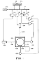
- Figure 1 is a schematic and diagrammatic view of an X-Y stage and an X-Y stage control circuit of an exposure apparatus according to an embodiment of the present invention.
- Figures 2A and 2B are graphs for explaining responsiveness of the X-Y stage to a designated value.
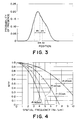
- Figure 3 is a graph for explaining a probability of presence in the position of the X-Y stage.
- Figure 4 is a graph for explaining the relation between a spatial frequency and a MTF.
- Figure 5 is a schematic and diagrammatic view of an exposure apparatus with a real time AA (autoalignment) function and a control circuit thereof, according to another embodiment of the present invention.
- AA autoalignment
- Figure 6 is a graph for explaining positional deviation between a reticle and a wafer during an exposure period.
- Figure 7 is a schematic view of a scanning exposure apparatus according to an embodiment of the present invention.
- Figure 8 is a graph for explaining a synchronism error between a reticle stage and a wafer stage during an exposure period.
- Figure 9 is a graph for explaining discrimination of positioning for a critical layer and a rough layer.
- Figures 10A and 10B are graphs for explaining attenuation of movement average of dispersion of vibration of the X-Y stage of Figure 1.
- Figure 11 is a time chart for explaining an exposure time and changes in dispersion of vibration of the X-Y stage of Figure 1.
- Figure 1 is a schematic and diagrammatic view of an X-Y stage and an X-Y stage control circuit according to an embodiment of the present invention.
- Denoted in Figure 1 at 101 is an X-Y stage, and denoted at 102 is a wafer chuck for holding a wafer 103.
- Denoted at 105 are X-axis motor and a Y-axis motor, and denoted at 107 are drivers for the motors 105.
- Denoted at 106 is a laser distance measuring device for detecting the position of the X-Y stage 101.
- Laser beam 108 emitted by the laser distance measuring device 106 is reflected by a mirror 104 fixedly mounted on the X-Y stage 101, and it enters again the laser distance measuring device 106 by which the position of the X-Y stage 101 is detected.
- Denoted at 109 is an off-axis type global alignment system in which, prior to the exposure process, the X-Y stage 101 moved to a site below the alignment system 109 and a positional deviation of an exposure pattern on the wafer 103 is measured beforehand. The result is reflected to a designation value for driving the stage for the exposure process.
- the X-Y stage control circuit includes a CPU 110 and a bus 111.
- a ROM 112 has a control program stored therein, and a RAM 113 serves to execute the control program or to store positional data.
- the CPU 110 As designation of a drive amount to the motor 105, the CPU 110 set a drive amount to a pulse generator 115 through the bus 111, and it is transmitted to the driver 107.
- the positional data from the laser distance measuring device 106 is transmitted to the CPU 110 or to the RAM 113, from an interface 114 and through the bus 111.
- Figure 2A shows the responsiveness of the X-Y stage 110 to a stepwise designated value.
- a designated value 201 changes stepwise, whereas a detected position 202 shows a delay at its rise and, after overshooting, it is converged and the exposure is done in time T of Figure 2A. High frequency vibration continues after convergence.
- Figure 2B is an enlarged view of a portion of the exposure time T in Figure 2A, and it shows a case where the detected position 202 converges gradually and a case where external vibration is applied. Such vibration adversely affects registration precision and resolution of exposure performance.
- Figure 3 shows a position change in Figure 2B in terms of probability of presence to position. It is illustrated that, to a designated value Xr in respect to X axis, a mean Xm is deviated.
- the mean Xm is represented by equation (1) below:
- Overall registration precision will be 60 nm in a case of 0.25 micron L&S (a pattern consisting of line and spaces of a width 0.25 micron) and 40 nm in a case of 0.15 micron L&S.
- the positioning precision of the X-Y stage 101 will be, for example, 10 nm in the case of 0.25 micron L&S and 6 nm in the case of 0.15 micron L&S.
- the standard deviation ⁇ x representing the dispersion degrades the resolution.
- the standard deviation ⁇ x is expressed by equation (2) below: Similarly, the same procedure will be taken in regard to the Y axis and any other axis.
- equations (1) and (2) should be rewritten as equations (3) and (4) below:
- MTF modulation transfer function
- Figure 4 illustrates that the MTF decreases with an increase in the spatial frequency and with enlargement of ⁇ .
- the spatial frequency u becomes equal to two per micron (2/micron).
- the positional information related to the X-Y stage 101 is stored, this being for executing error shot discrimination just after completion of the exposure. More specifically, the sampling is carried out with a rate twice or more of a major frequency component of vibration.
- the error shot discrimination is made. Also, the exposure specifications at Table 1 are those for a critical layer. There is a wider tolerance for rough layers.
- a different driving portion which may be a source of external disturbance during the exposure process, such as a conveying system, for example, may be actuated during the exposure process, this being effective to enhance the throughput. Further, if the exposure time is longer, the operation time of the driving portion may be prolonged.
- FIG. 5 is a block diagram of a control circuit of an exposure apparatus having a real time AA function, according to another embodiment of the present invention.
- Denoted in Figure 5 at 501 is an exposure light source, and denoted at 502 is a reticle.
- Denoted at 503 is a lens optical system, and denoted at 504 are pickups for detecting a positional deviation between the reticle 502 and a wafer 103 in real time fashion. Detection signals from the pickups 504 are transformed by an AA unit 510 into positional information which is applied to the CPU 110 or RAM 113 through the bus 111.
- Figure 6 shows a result of detection of positional deviation, obtained by real time autoalignment, and it illustrates changes in a positional deviation 602 to a designated value 601 during the exposure time T.
- the error shot discrimination is made by determining a standard deviation and a mean in relation to respective axes on the basis of the resultant data. Since in this embodiment the relative position of the reticle 502 and the wafer 103 is detected, more accurate error shot discrimination is attainable in this embodiment as compared with the preceding embodiment.
- Figure 7 shows the structure of a scanning exposure apparatus according to an embodiment of the present invention.
- a reticle stage 701 and a wafer stage 101 are moved in a timed relation by which enlargement of exposure view angle is attained with a small diameter lens.
- magnification or exposure amount within the view angle becomes non-uniform.
- laser distance measuring devices 106 are used to detect the positions of the reticle stage 701 and the wafer stage 101, and theses stages are driven by their motors 105 while feeding back their positional deviations.
- Figure 8 illustrates a synchronism error 802 to a designated value 801 for the reticle stage 701 and the wafer stage 101 during the exposure time in the real time AA control, or to the laser distance measuring device 106.
- scan axis alignment is particularly difficult to achieve. Therefore, executing the error shot discrimination by taking a standard deviation and mean of respective axis in this embodiment, like the preceding embodiment or embodiments, is very effective.
- Figure 9 illustrates the manner of positioning discrimination for an X-Y stage 101, for a rough layer and a critical layer.
- the positioning is completed when the level is held within a threshold range ⁇ for a predetermined period t a , after the level comes into the threshold range ⁇ .
- the threshold ⁇ is determined in accordance with the layer. It is ⁇ r for rough layers, and it is ⁇ c for critical layers.
- Such threshold is given by about three times the tolerable amplitude ( ⁇ ), naturally there is a relation ⁇ r > ⁇ c.
- the time from change of designated value to completion of positioning is given, in respect to respective layers, by t sr and t sc and, naturally, there is a relation t sr ⁇ t sc .
- the positioning time can be reduced and the throughput can be enhanced.
- Figure 10A illustrates at 601 the change in a value of square of the difference between the designated value 201 and the detected position 201 in Figure 9. Depicted at 602 is movement average of the square 601, and it represents change in dispersion. The moment of rise of the dispersion 602 is denoted by 0, and the moment of a peak value of dispersion 602 is denoted by tp.
- Figure 10B shows in enlarged scale a portion of Figure 10A in which the dispersion 602 gradually decreases after the time tp.
- D a constant of attenuation
- Vr represents dispersion of residual vibration which is measured beforehand.
- movement average of dispersion is measured successively and discrimination is made as to whether the result corresponds to which portion of the approximation curve, and then the time necessary for convergence to desired vibration amplitude is calculated.
- equation (8) follows and the exposure start moment ts is determined by tolerable dispersion Vm and exposure time T: ts ⁇ tp+T/(exp(Vm-Vr)T/D)-1)
- Figure 11 is a time chart of exposure time and changes in dispersion of vibration.
- the time from start of attenuation of vibration to start of exposure can be reduced much more if the design rule L&S is larger and the exposure time T is longer.
- the shortening effect of time is larger with longer exposure time, and the throughput enhancement is bigger.
- equation (9) may be calculated beforehand and, when the movement average of dispersion becomes not more than that value, the exposure may be started. This provides substantially the same advantageous results as the preceding embodiments.
- the alignment method and exposure method can be used in the manufacture of semiconductor devices. Errors in alignment are detected after exposure to determine any shot errors. The areas of the substrate which have been correctly and accurately exposed to the shot pattern can then be used for the fabrication of semiconductor devices using conventional well known techniques.
Landscapes
- Physics & Mathematics (AREA)
- General Physics & Mathematics (AREA)
- Health & Medical Sciences (AREA)
- Life Sciences & Earth Sciences (AREA)
- Atmospheric Sciences (AREA)
- Toxicology (AREA)
- Engineering & Computer Science (AREA)
- Environmental & Geological Engineering (AREA)
- Epidemiology (AREA)
- Public Health (AREA)
- Exposure And Positioning Against Photoresist Photosensitive Materials (AREA)
- Exposure Of Semiconductors, Excluding Electron Or Ion Beam Exposure (AREA)
Priority Applications (1)
| Application Number | Priority Date | Filing Date | Title |
|---|---|---|---|
| EP00200725A EP1016931B1 (de) | 1995-08-30 | 1996-08-29 | Belichtungsapparat und -verfahren unter Verwendung einer Bewertung der Positionierung einer Trägerplatte |
Applications Claiming Priority (6)
| Application Number | Priority Date | Filing Date | Title |
|---|---|---|---|
| JP24398095 | 1995-08-30 | ||
| JP243980/95 | 1995-08-30 | ||
| JP24398095A JP3501564B2 (ja) | 1995-08-30 | 1995-08-30 | 走査型露光装置及びエラーショット判別方法 |
| JP1923696 | 1996-01-11 | ||
| JP19236/96 | 1996-01-11 | ||
| JP01923696A JP3313962B2 (ja) | 1996-01-11 | 1996-01-11 | 整定判定方法及びそれを用いた露光装置 |
Related Child Applications (1)
| Application Number | Title | Priority Date | Filing Date |
|---|---|---|---|
| EP00200725A Division EP1016931B1 (de) | 1995-08-30 | 1996-08-29 | Belichtungsapparat und -verfahren unter Verwendung einer Bewertung der Positionierung einer Trägerplatte |
Publications (3)
| Publication Number | Publication Date |
|---|---|
| EP0762216A2 true EP0762216A2 (de) | 1997-03-12 |
| EP0762216A3 EP0762216A3 (de) | 1998-04-08 |
| EP0762216B1 EP0762216B1 (de) | 2002-01-02 |
Family
ID=26356068
Family Applications (2)
| Application Number | Title | Priority Date | Filing Date |
|---|---|---|---|
| EP00200725A Expired - Lifetime EP1016931B1 (de) | 1995-08-30 | 1996-08-29 | Belichtungsapparat und -verfahren unter Verwendung einer Bewertung der Positionierung einer Trägerplatte |
| EP96306266A Expired - Lifetime EP0762216B1 (de) | 1995-08-30 | 1996-08-29 | Belichtungsvorrichtung und Verfahren zur Bewertung einer Ausrichtung |
Family Applications Before (1)
| Application Number | Title | Priority Date | Filing Date |
|---|---|---|---|
| EP00200725A Expired - Lifetime EP1016931B1 (de) | 1995-08-30 | 1996-08-29 | Belichtungsapparat und -verfahren unter Verwendung einer Bewertung der Positionierung einer Trägerplatte |
Country Status (4)
| Country | Link |
|---|---|
| US (1) | US5760878A (de) |
| EP (2) | EP1016931B1 (de) |
| KR (1) | KR100232906B1 (de) |
| DE (2) | DE69637133D1 (de) |
Families Citing this family (5)
| Publication number | Priority date | Publication date | Assignee | Title |
|---|---|---|---|---|
| JPH09115799A (ja) | 1995-10-16 | 1997-05-02 | Nikon Corp | 走査型露光装置 |
| KR100317580B1 (ko) * | 1998-06-01 | 2002-04-24 | 박종섭 | 노광시스템 |
| JP3548428B2 (ja) * | 1998-07-03 | 2004-07-28 | キヤノン株式会社 | 位置計測装置及びそれを用いたデバイスの製造方法 |
| KR100576818B1 (ko) * | 1999-12-13 | 2006-05-10 | 삼성전자주식회사 | 노광 장비의 웨이퍼 매칭 시스템 및 그 제어 방법 |
| JP6066592B2 (ja) | 2012-06-12 | 2017-01-25 | キヤノン株式会社 | 露光装置及びデバイス製造方法 |
Family Cites Families (6)
| Publication number | Priority date | Publication date | Assignee | Title |
|---|---|---|---|---|
| JPS5994419A (ja) * | 1982-11-19 | 1984-05-31 | Canon Inc | 分割焼付け装置におけるアライメント方法 |
| JPS6032050A (ja) * | 1983-08-02 | 1985-02-19 | Canon Inc | 露光装置 |
| DE69123610T2 (de) * | 1990-02-02 | 1997-04-24 | Canon K.K., Tokio/Tokyo | Belichtungsverfahren |
| JPH05136023A (ja) * | 1991-11-14 | 1993-06-01 | Nikon Corp | 投影露光装置 |
| JPH07260472A (ja) * | 1994-03-22 | 1995-10-13 | Nikon Corp | ステージ装置の直交度測定方法 |
| JP3448991B2 (ja) * | 1994-11-29 | 2003-09-22 | 株式会社ニコン | ステージ移動制御装置、投影型露光装置およびステージ駆動方法ならびに露光方法。 |
-
1996
- 1996-08-23 US US08/702,326 patent/US5760878A/en not_active Expired - Lifetime
- 1996-08-29 DE DE69637133T patent/DE69637133D1/de not_active Expired - Lifetime
- 1996-08-29 EP EP00200725A patent/EP1016931B1/de not_active Expired - Lifetime
- 1996-08-29 EP EP96306266A patent/EP0762216B1/de not_active Expired - Lifetime
- 1996-08-29 DE DE69618301T patent/DE69618301T2/de not_active Expired - Lifetime
- 1996-08-30 KR KR1019960036633A patent/KR100232906B1/ko not_active Expired - Fee Related
Also Published As
| Publication number | Publication date |
|---|---|
| EP0762216B1 (de) | 2002-01-02 |
| EP1016931A1 (de) | 2000-07-05 |
| DE69618301D1 (de) | 2002-02-07 |
| EP1016931B1 (de) | 2007-06-13 |
| US5760878A (en) | 1998-06-02 |
| KR100232906B1 (ko) | 1999-12-01 |
| EP0762216A3 (de) | 1998-04-08 |
| DE69637133D1 (de) | 2007-07-26 |
| KR970012983A (ko) | 1997-03-29 |
| DE69618301T2 (de) | 2002-06-27 |
Similar Documents
| Publication | Publication Date | Title |
|---|---|---|
| EP1413928B1 (de) | Vorrichtung und Verfahren zur Abtastbelichtung | |
| JP3181050B2 (ja) | 投影露光方法およびその装置 | |
| US5502311A (en) | Method of and apparatus for detecting plane position | |
| US6333786B1 (en) | Aligning method | |
| US5805866A (en) | Alignment method | |
| EP1195647B1 (de) | Verfahren zur Detektion einer Oberflächenlage und Abtastbelichtungsverfahren unter Verwendung derselbe | |
| US6424405B2 (en) | Exposure apparatus and device manufacturing method | |
| US6501532B2 (en) | Exposure apparatus and method of controlling the same | |
| EP0130819A2 (de) | Verfahren für die Positionierung eines Strahles an einem bestimmten Teil einer Halbleiterscheibe | |
| US5361122A (en) | Autofocusing device and projection exposure apparatus with the same | |
| EP0740215B1 (de) | Abtastbelichtungsapparat und Belichtungsverfahren unter Verwendung desselben | |
| US5134298A (en) | Beam control method and apparatus | |
| EP0762216A2 (de) | Belichtungsverfahren und -vorrichtung und Verfahren und Vorrichtung zur Bewertung einer Ausrichtung | |
| US6476904B1 (en) | Projection exposure method and apparatus | |
| EP0338200B1 (de) | Verfahren und Gerät zur Charakterisierung von optischen Systemen | |
| US6816239B2 (en) | Exposure apparatus, method of controlling same, and method of manufacturing devices | |
| JP2001143991A (ja) | 面位置検出装置およびデバイス製造方法 | |
| EP0474445B1 (de) | Automatische Fokussierungsvorrichtung und Projektionsbelichtungsgerät mit einer solchen Anordnung | |
| KR100317092B1 (ko) | 주사형노광장치및디바이스제조방법 | |
| KR100257132B1 (ko) | 슬릿 스캔식 투영 노광 장치와 투영 노광 방법 및 이것을 이용한 반도체 장치의 제조 방법 | |
| JP2705778B2 (ja) | 投影露光装置 | |
| JP4598902B2 (ja) | 走査露光装置およびデバイス製造方法 | |
| US6337486B2 (en) | Electron beam drawing process and electron beam drawing apparatus | |
| JP3501564B2 (ja) | 走査型露光装置及びエラーショット判別方法 | |
| JP3313962B2 (ja) | 整定判定方法及びそれを用いた露光装置 |
Legal Events
| Date | Code | Title | Description |
|---|---|---|---|
| PUAI | Public reference made under article 153(3) epc to a published international application that has entered the european phase |
Free format text: ORIGINAL CODE: 0009012 |
|
| AK | Designated contracting states |
Kind code of ref document: A2 Designated state(s): DE GB NL |
|
| PUAL | Search report despatched |
Free format text: ORIGINAL CODE: 0009013 |
|
| AK | Designated contracting states |
Kind code of ref document: A3 Designated state(s): DE GB NL |
|
| 17P | Request for examination filed |
Effective date: 19980820 |
|
| 17Q | First examination report despatched |
Effective date: 19980918 |
|
| RTI1 | Title (correction) |
Free format text: EXPOSURE APPARATUS AND ALIGNMENT EVALUATION METHOD |
|
| GRAG | Despatch of communication of intention to grant |
Free format text: ORIGINAL CODE: EPIDOS AGRA |
|
| GRAG | Despatch of communication of intention to grant |
Free format text: ORIGINAL CODE: EPIDOS AGRA |
|
| GRAG | Despatch of communication of intention to grant |
Free format text: ORIGINAL CODE: EPIDOS AGRA |
|
| RTI1 | Title (correction) |
Free format text: EXPOSURE APPARATUS AND ALIGNMENT EVALUATION METHOD |
|
| GRAG | Despatch of communication of intention to grant |
Free format text: ORIGINAL CODE: EPIDOS AGRA |
|
| GRAH | Despatch of communication of intention to grant a patent |
Free format text: ORIGINAL CODE: EPIDOS IGRA |
|
| GRAH | Despatch of communication of intention to grant a patent |
Free format text: ORIGINAL CODE: EPIDOS IGRA |
|
| GRAA | (expected) grant |
Free format text: ORIGINAL CODE: 0009210 |
|
| REG | Reference to a national code |
Ref country code: GB Ref legal event code: IF02 |
|
| AK | Designated contracting states |
Kind code of ref document: B1 Designated state(s): DE GB NL |
|
| REF | Corresponds to: |
Ref document number: 69618301 Country of ref document: DE Date of ref document: 20020207 |
|
| PLBE | No opposition filed within time limit |
Free format text: ORIGINAL CODE: 0009261 |
|
| STAA | Information on the status of an ep patent application or granted ep patent |
Free format text: STATUS: NO OPPOSITION FILED WITHIN TIME LIMIT |
|
| 26N | No opposition filed | ||
| PGFP | Annual fee paid to national office [announced via postgrant information from national office to epo] |
Ref country code: NL Payment date: 20080819 Year of fee payment: 13 |
|
| REG | Reference to a national code |
Ref country code: NL Ref legal event code: V1 Effective date: 20100301 |
|
| PG25 | Lapsed in a contracting state [announced via postgrant information from national office to epo] |
Ref country code: NL Free format text: LAPSE BECAUSE OF NON-PAYMENT OF DUE FEES Effective date: 20100301 |
|
| PGFP | Annual fee paid to national office [announced via postgrant information from national office to epo] |
Ref country code: DE Payment date: 20140831 Year of fee payment: 19 |
|
| PGFP | Annual fee paid to national office [announced via postgrant information from national office to epo] |
Ref country code: GB Payment date: 20140822 Year of fee payment: 19 |
|
| REG | Reference to a national code |
Ref country code: DE Ref legal event code: R119 Ref document number: 69618301 Country of ref document: DE |
|
| GBPC | Gb: european patent ceased through non-payment of renewal fee |
Effective date: 20150829 |
|
| PG25 | Lapsed in a contracting state [announced via postgrant information from national office to epo] |
Ref country code: GB Free format text: LAPSE BECAUSE OF NON-PAYMENT OF DUE FEES Effective date: 20150829 Ref country code: DE Free format text: LAPSE BECAUSE OF NON-PAYMENT OF DUE FEES Effective date: 20160301 |