EP0762373B1 - Plasma-Anzeigetafel, Verfahren zu ihrer Ansteuerung, um Anzeige mit Zeilensprung durchzuführen, und Plasma-Anzeigegerät - Google Patents
Plasma-Anzeigetafel, Verfahren zu ihrer Ansteuerung, um Anzeige mit Zeilensprung durchzuführen, und Plasma-Anzeigegerät Download PDFInfo
- Publication number
- EP0762373B1 EP0762373B1 EP96305776A EP96305776A EP0762373B1 EP 0762373 B1 EP0762373 B1 EP 0762373B1 EP 96305776 A EP96305776 A EP 96305776A EP 96305776 A EP96305776 A EP 96305776A EP 0762373 B1 EP0762373 B1 EP 0762373B1
- Authority
- EP
- European Patent Office
- Prior art keywords
- electrodes
- electrode
- numbered
- discharge
- sustaining
- Prior art date
- Legal status (The legal status is an assumption and is not a legal conclusion. Google has not performed a legal analysis and makes no representation as to the accuracy of the status listed.)
- Expired - Lifetime
Links
Images


Classifications
-
- H—ELECTRICITY
- H01—ELECTRIC ELEMENTS
- H01J—ELECTRIC DISCHARGE TUBES OR DISCHARGE LAMPS
- H01J11/00—Gas-filled discharge tubes with alternating current induction of the discharge, e.g. alternating current plasma display panels [AC-PDP]; Gas-filled discharge tubes without any main electrode inside the vessel; Gas-filled discharge tubes with at least one main electrode outside the vessel
- H01J11/20—Constructional details
- H01J11/22—Electrodes, e.g. special shape, material or configuration
- H01J11/28—Auxiliary electrodes, e.g. priming electrodes or trigger electrodes
-
- G—PHYSICS
- G09—EDUCATION; CRYPTOGRAPHY; DISPLAY; ADVERTISING; SEALS
- G09G—ARRANGEMENTS OR CIRCUITS FOR CONTROL OF INDICATING DEVICES USING STATIC MEANS TO PRESENT VARIABLE INFORMATION
- G09G3/00—Control arrangements or circuits, of interest only in connection with visual indicators other than cathode-ray tubes
- G09G3/20—Control arrangements or circuits, of interest only in connection with visual indicators other than cathode-ray tubes for presentation of an assembly of a number of characters, e.g. a page, by composing the assembly by combination of individual elements arranged in a matrix no fixed position being assigned to or needed to be assigned to the individual characters or partial characters
- G09G3/22—Control arrangements or circuits, of interest only in connection with visual indicators other than cathode-ray tubes for presentation of an assembly of a number of characters, e.g. a page, by composing the assembly by combination of individual elements arranged in a matrix no fixed position being assigned to or needed to be assigned to the individual characters or partial characters using controlled light sources
- G09G3/28—Control arrangements or circuits, of interest only in connection with visual indicators other than cathode-ray tubes for presentation of an assembly of a number of characters, e.g. a page, by composing the assembly by combination of individual elements arranged in a matrix no fixed position being assigned to or needed to be assigned to the individual characters or partial characters using controlled light sources using luminous gas-discharge panels, e.g. plasma panels
- G09G3/288—Control arrangements or circuits, of interest only in connection with visual indicators other than cathode-ray tubes for presentation of an assembly of a number of characters, e.g. a page, by composing the assembly by combination of individual elements arranged in a matrix no fixed position being assigned to or needed to be assigned to the individual characters or partial characters using controlled light sources using luminous gas-discharge panels, e.g. plasma panels using AC panels
- G09G3/291—Control arrangements or circuits, of interest only in connection with visual indicators other than cathode-ray tubes for presentation of an assembly of a number of characters, e.g. a page, by composing the assembly by combination of individual elements arranged in a matrix no fixed position being assigned to or needed to be assigned to the individual characters or partial characters using controlled light sources using luminous gas-discharge panels, e.g. plasma panels using AC panels controlling the gas discharge to control a cell condition, e.g. by means of specific pulse shapes
- G09G3/293—Control arrangements or circuits, of interest only in connection with visual indicators other than cathode-ray tubes for presentation of an assembly of a number of characters, e.g. a page, by composing the assembly by combination of individual elements arranged in a matrix no fixed position being assigned to or needed to be assigned to the individual characters or partial characters using controlled light sources using luminous gas-discharge panels, e.g. plasma panels using AC panels controlling the gas discharge to control a cell condition, e.g. by means of specific pulse shapes for address discharge
- G09G3/2932—Addressed by writing selected cells that are in an OFF state
-
- G—PHYSICS
- G09—EDUCATION; CRYPTOGRAPHY; DISPLAY; ADVERTISING; SEALS
- G09G—ARRANGEMENTS OR CIRCUITS FOR CONTROL OF INDICATING DEVICES USING STATIC MEANS TO PRESENT VARIABLE INFORMATION
- G09G3/00—Control arrangements or circuits, of interest only in connection with visual indicators other than cathode-ray tubes
- G09G3/20—Control arrangements or circuits, of interest only in connection with visual indicators other than cathode-ray tubes for presentation of an assembly of a number of characters, e.g. a page, by composing the assembly by combination of individual elements arranged in a matrix no fixed position being assigned to or needed to be assigned to the individual characters or partial characters
- G09G3/22—Control arrangements or circuits, of interest only in connection with visual indicators other than cathode-ray tubes for presentation of an assembly of a number of characters, e.g. a page, by composing the assembly by combination of individual elements arranged in a matrix no fixed position being assigned to or needed to be assigned to the individual characters or partial characters using controlled light sources
- G09G3/28—Control arrangements or circuits, of interest only in connection with visual indicators other than cathode-ray tubes for presentation of an assembly of a number of characters, e.g. a page, by composing the assembly by combination of individual elements arranged in a matrix no fixed position being assigned to or needed to be assigned to the individual characters or partial characters using controlled light sources using luminous gas-discharge panels, e.g. plasma panels
- G09G3/288—Control arrangements or circuits, of interest only in connection with visual indicators other than cathode-ray tubes for presentation of an assembly of a number of characters, e.g. a page, by composing the assembly by combination of individual elements arranged in a matrix no fixed position being assigned to or needed to be assigned to the individual characters or partial characters using controlled light sources using luminous gas-discharge panels, e.g. plasma panels using AC panels
- G09G3/291—Control arrangements or circuits, of interest only in connection with visual indicators other than cathode-ray tubes for presentation of an assembly of a number of characters, e.g. a page, by composing the assembly by combination of individual elements arranged in a matrix no fixed position being assigned to or needed to be assigned to the individual characters or partial characters using controlled light sources using luminous gas-discharge panels, e.g. plasma panels using AC panels controlling the gas discharge to control a cell condition, e.g. by means of specific pulse shapes
- G09G3/294—Control arrangements or circuits, of interest only in connection with visual indicators other than cathode-ray tubes for presentation of an assembly of a number of characters, e.g. a page, by composing the assembly by combination of individual elements arranged in a matrix no fixed position being assigned to or needed to be assigned to the individual characters or partial characters using controlled light sources using luminous gas-discharge panels, e.g. plasma panels using AC panels controlling the gas discharge to control a cell condition, e.g. by means of specific pulse shapes for lighting or sustain discharge
- G09G3/2948—Control arrangements or circuits, of interest only in connection with visual indicators other than cathode-ray tubes for presentation of an assembly of a number of characters, e.g. a page, by composing the assembly by combination of individual elements arranged in a matrix no fixed position being assigned to or needed to be assigned to the individual characters or partial characters using controlled light sources using luminous gas-discharge panels, e.g. plasma panels using AC panels controlling the gas discharge to control a cell condition, e.g. by means of specific pulse shapes for lighting or sustain discharge by increasing the total sustaining time with respect to other times in the frame
-
- G—PHYSICS
- G09—EDUCATION; CRYPTOGRAPHY; DISPLAY; ADVERTISING; SEALS
- G09G—ARRANGEMENTS OR CIRCUITS FOR CONTROL OF INDICATING DEVICES USING STATIC MEANS TO PRESENT VARIABLE INFORMATION
- G09G3/00—Control arrangements or circuits, of interest only in connection with visual indicators other than cathode-ray tubes
- G09G3/20—Control arrangements or circuits, of interest only in connection with visual indicators other than cathode-ray tubes for presentation of an assembly of a number of characters, e.g. a page, by composing the assembly by combination of individual elements arranged in a matrix no fixed position being assigned to or needed to be assigned to the individual characters or partial characters
- G09G3/22—Control arrangements or circuits, of interest only in connection with visual indicators other than cathode-ray tubes for presentation of an assembly of a number of characters, e.g. a page, by composing the assembly by combination of individual elements arranged in a matrix no fixed position being assigned to or needed to be assigned to the individual characters or partial characters using controlled light sources
- G09G3/28—Control arrangements or circuits, of interest only in connection with visual indicators other than cathode-ray tubes for presentation of an assembly of a number of characters, e.g. a page, by composing the assembly by combination of individual elements arranged in a matrix no fixed position being assigned to or needed to be assigned to the individual characters or partial characters using controlled light sources using luminous gas-discharge panels, e.g. plasma panels
- G09G3/288—Control arrangements or circuits, of interest only in connection with visual indicators other than cathode-ray tubes for presentation of an assembly of a number of characters, e.g. a page, by composing the assembly by combination of individual elements arranged in a matrix no fixed position being assigned to or needed to be assigned to the individual characters or partial characters using controlled light sources using luminous gas-discharge panels, e.g. plasma panels using AC panels
- G09G3/296—Driving circuits for producing the waveforms applied to the driving electrodes
-
- G—PHYSICS
- G09—EDUCATION; CRYPTOGRAPHY; DISPLAY; ADVERTISING; SEALS
- G09G—ARRANGEMENTS OR CIRCUITS FOR CONTROL OF INDICATING DEVICES USING STATIC MEANS TO PRESENT VARIABLE INFORMATION
- G09G3/00—Control arrangements or circuits, of interest only in connection with visual indicators other than cathode-ray tubes
- G09G3/20—Control arrangements or circuits, of interest only in connection with visual indicators other than cathode-ray tubes for presentation of an assembly of a number of characters, e.g. a page, by composing the assembly by combination of individual elements arranged in a matrix no fixed position being assigned to or needed to be assigned to the individual characters or partial characters
- G09G3/22—Control arrangements or circuits, of interest only in connection with visual indicators other than cathode-ray tubes for presentation of an assembly of a number of characters, e.g. a page, by composing the assembly by combination of individual elements arranged in a matrix no fixed position being assigned to or needed to be assigned to the individual characters or partial characters using controlled light sources
- G09G3/28—Control arrangements or circuits, of interest only in connection with visual indicators other than cathode-ray tubes for presentation of an assembly of a number of characters, e.g. a page, by composing the assembly by combination of individual elements arranged in a matrix no fixed position being assigned to or needed to be assigned to the individual characters or partial characters using controlled light sources using luminous gas-discharge panels, e.g. plasma panels
- G09G3/288—Control arrangements or circuits, of interest only in connection with visual indicators other than cathode-ray tubes for presentation of an assembly of a number of characters, e.g. a page, by composing the assembly by combination of individual elements arranged in a matrix no fixed position being assigned to or needed to be assigned to the individual characters or partial characters using controlled light sources using luminous gas-discharge panels, e.g. plasma panels using AC panels
- G09G3/298—Control arrangements or circuits, of interest only in connection with visual indicators other than cathode-ray tubes for presentation of an assembly of a number of characters, e.g. a page, by composing the assembly by combination of individual elements arranged in a matrix no fixed position being assigned to or needed to be assigned to the individual characters or partial characters using controlled light sources using luminous gas-discharge panels, e.g. plasma panels using AC panels using surface discharge panels
- G09G3/2983—Control arrangements or circuits, of interest only in connection with visual indicators other than cathode-ray tubes for presentation of an assembly of a number of characters, e.g. a page, by composing the assembly by combination of individual elements arranged in a matrix no fixed position being assigned to or needed to be assigned to the individual characters or partial characters using controlled light sources using luminous gas-discharge panels, e.g. plasma panels using AC panels using surface discharge panels using non-standard pixel electrode arrangements
-
- G—PHYSICS
- G09—EDUCATION; CRYPTOGRAPHY; DISPLAY; ADVERTISING; SEALS
- G09G—ARRANGEMENTS OR CIRCUITS FOR CONTROL OF INDICATING DEVICES USING STATIC MEANS TO PRESENT VARIABLE INFORMATION
- G09G3/00—Control arrangements or circuits, of interest only in connection with visual indicators other than cathode-ray tubes
- G09G3/20—Control arrangements or circuits, of interest only in connection with visual indicators other than cathode-ray tubes for presentation of an assembly of a number of characters, e.g. a page, by composing the assembly by combination of individual elements arranged in a matrix no fixed position being assigned to or needed to be assigned to the individual characters or partial characters
- G09G3/22—Control arrangements or circuits, of interest only in connection with visual indicators other than cathode-ray tubes for presentation of an assembly of a number of characters, e.g. a page, by composing the assembly by combination of individual elements arranged in a matrix no fixed position being assigned to or needed to be assigned to the individual characters or partial characters using controlled light sources
- G09G3/28—Control arrangements or circuits, of interest only in connection with visual indicators other than cathode-ray tubes for presentation of an assembly of a number of characters, e.g. a page, by composing the assembly by combination of individual elements arranged in a matrix no fixed position being assigned to or needed to be assigned to the individual characters or partial characters using controlled light sources using luminous gas-discharge panels, e.g. plasma panels
- G09G3/288—Control arrangements or circuits, of interest only in connection with visual indicators other than cathode-ray tubes for presentation of an assembly of a number of characters, e.g. a page, by composing the assembly by combination of individual elements arranged in a matrix no fixed position being assigned to or needed to be assigned to the individual characters or partial characters using controlled light sources using luminous gas-discharge panels, e.g. plasma panels using AC panels
- G09G3/298—Control arrangements or circuits, of interest only in connection with visual indicators other than cathode-ray tubes for presentation of an assembly of a number of characters, e.g. a page, by composing the assembly by combination of individual elements arranged in a matrix no fixed position being assigned to or needed to be assigned to the individual characters or partial characters using controlled light sources using luminous gas-discharge panels, e.g. plasma panels using AC panels using surface discharge panels
- G09G3/299—Control arrangements or circuits, of interest only in connection with visual indicators other than cathode-ray tubes for presentation of an assembly of a number of characters, e.g. a page, by composing the assembly by combination of individual elements arranged in a matrix no fixed position being assigned to or needed to be assigned to the individual characters or partial characters using controlled light sources using luminous gas-discharge panels, e.g. plasma panels using AC panels using surface discharge panels using alternate lighting of surface-type panels
-
- H—ELECTRICITY
- H01—ELECTRIC ELEMENTS
- H01J—ELECTRIC DISCHARGE TUBES OR DISCHARGE LAMPS
- H01J11/00—Gas-filled discharge tubes with alternating current induction of the discharge, e.g. alternating current plasma display panels [AC-PDP]; Gas-filled discharge tubes without any main electrode inside the vessel; Gas-filled discharge tubes with at least one main electrode outside the vessel
- H01J11/10—AC-PDPs with at least one main electrode being out of contact with the plasma
- H01J11/12—AC-PDPs with at least one main electrode being out of contact with the plasma with main electrodes provided on both sides of the discharge space
-
- H—ELECTRICITY
- H01—ELECTRIC ELEMENTS
- H01J—ELECTRIC DISCHARGE TUBES OR DISCHARGE LAMPS
- H01J11/00—Gas-filled discharge tubes with alternating current induction of the discharge, e.g. alternating current plasma display panels [AC-PDP]; Gas-filled discharge tubes without any main electrode inside the vessel; Gas-filled discharge tubes with at least one main electrode outside the vessel
- H01J11/20—Constructional details
- H01J11/34—Vessels, containers or parts thereof, e.g. substrates
- H01J11/44—Optical arrangements or shielding arrangements, e.g. filters, black matrices, light reflecting means or electromagnetic shielding means
-
- G—PHYSICS
- G09—EDUCATION; CRYPTOGRAPHY; DISPLAY; ADVERTISING; SEALS
- G09G—ARRANGEMENTS OR CIRCUITS FOR CONTROL OF INDICATING DEVICES USING STATIC MEANS TO PRESENT VARIABLE INFORMATION
- G09G2230/00—Details of flat display driving waveforms
-
- G—PHYSICS
- G09—EDUCATION; CRYPTOGRAPHY; DISPLAY; ADVERTISING; SEALS
- G09G—ARRANGEMENTS OR CIRCUITS FOR CONTROL OF INDICATING DEVICES USING STATIC MEANS TO PRESENT VARIABLE INFORMATION
- G09G2310/00—Command of the display device
- G09G2310/02—Addressing, scanning or driving the display screen or processing steps related thereto
- G09G2310/0202—Addressing of scan or signal lines
- G09G2310/0205—Simultaneous scanning of several lines in flat panels
-
- G—PHYSICS
- G09—EDUCATION; CRYPTOGRAPHY; DISPLAY; ADVERTISING; SEALS
- G09G—ARRANGEMENTS OR CIRCUITS FOR CONTROL OF INDICATING DEVICES USING STATIC MEANS TO PRESENT VARIABLE INFORMATION
- G09G2310/00—Command of the display device
- G09G2310/02—Addressing, scanning or driving the display screen or processing steps related thereto
- G09G2310/0202—Addressing of scan or signal lines
- G09G2310/0218—Addressing of scan or signal lines with collection of electrodes in groups for n-dimensional addressing
-
- G—PHYSICS
- G09—EDUCATION; CRYPTOGRAPHY; DISPLAY; ADVERTISING; SEALS
- G09G—ARRANGEMENTS OR CIRCUITS FOR CONTROL OF INDICATING DEVICES USING STATIC MEANS TO PRESENT VARIABLE INFORMATION
- G09G2310/00—Command of the display device
- G09G2310/02—Addressing, scanning or driving the display screen or processing steps related thereto
- G09G2310/0202—Addressing of scan or signal lines
- G09G2310/0221—Addressing of scan or signal lines with use of split matrices
-
- G—PHYSICS
- G09—EDUCATION; CRYPTOGRAPHY; DISPLAY; ADVERTISING; SEALS
- G09G—ARRANGEMENTS OR CIRCUITS FOR CONTROL OF INDICATING DEVICES USING STATIC MEANS TO PRESENT VARIABLE INFORMATION
- G09G2310/00—Command of the display device
- G09G2310/02—Addressing, scanning or driving the display screen or processing steps related thereto
- G09G2310/0224—Details of interlacing
-
- G—PHYSICS
- G09—EDUCATION; CRYPTOGRAPHY; DISPLAY; ADVERTISING; SEALS
- G09G—ARRANGEMENTS OR CIRCUITS FOR CONTROL OF INDICATING DEVICES USING STATIC MEANS TO PRESENT VARIABLE INFORMATION
- G09G2330/00—Aspects of power supply; Aspects of display protection and defect management
- G09G2330/02—Details of power systems and of start or stop of display operation
- G09G2330/021—Power management, e.g. power saving
-
- G—PHYSICS
- G09—EDUCATION; CRYPTOGRAPHY; DISPLAY; ADVERTISING; SEALS
- G09G—ARRANGEMENTS OR CIRCUITS FOR CONTROL OF INDICATING DEVICES USING STATIC MEANS TO PRESENT VARIABLE INFORMATION
- G09G3/00—Control arrangements or circuits, of interest only in connection with visual indicators other than cathode-ray tubes
- G09G3/20—Control arrangements or circuits, of interest only in connection with visual indicators other than cathode-ray tubes for presentation of an assembly of a number of characters, e.g. a page, by composing the assembly by combination of individual elements arranged in a matrix no fixed position being assigned to or needed to be assigned to the individual characters or partial characters
- G09G3/2007—Display of intermediate tones
- G09G3/2018—Display of intermediate tones by time modulation using two or more time intervals
-
- G—PHYSICS
- G09—EDUCATION; CRYPTOGRAPHY; DISPLAY; ADVERTISING; SEALS
- G09G—ARRANGEMENTS OR CIRCUITS FOR CONTROL OF INDICATING DEVICES USING STATIC MEANS TO PRESENT VARIABLE INFORMATION
- G09G3/00—Control arrangements or circuits, of interest only in connection with visual indicators other than cathode-ray tubes
- G09G3/20—Control arrangements or circuits, of interest only in connection with visual indicators other than cathode-ray tubes for presentation of an assembly of a number of characters, e.g. a page, by composing the assembly by combination of individual elements arranged in a matrix no fixed position being assigned to or needed to be assigned to the individual characters or partial characters
- G09G3/22—Control arrangements or circuits, of interest only in connection with visual indicators other than cathode-ray tubes for presentation of an assembly of a number of characters, e.g. a page, by composing the assembly by combination of individual elements arranged in a matrix no fixed position being assigned to or needed to be assigned to the individual characters or partial characters using controlled light sources
- G09G3/28—Control arrangements or circuits, of interest only in connection with visual indicators other than cathode-ray tubes for presentation of an assembly of a number of characters, e.g. a page, by composing the assembly by combination of individual elements arranged in a matrix no fixed position being assigned to or needed to be assigned to the individual characters or partial characters using controlled light sources using luminous gas-discharge panels, e.g. plasma panels
- G09G3/288—Control arrangements or circuits, of interest only in connection with visual indicators other than cathode-ray tubes for presentation of an assembly of a number of characters, e.g. a page, by composing the assembly by combination of individual elements arranged in a matrix no fixed position being assigned to or needed to be assigned to the individual characters or partial characters using controlled light sources using luminous gas-discharge panels, e.g. plasma panels using AC panels
- G09G3/291—Control arrangements or circuits, of interest only in connection with visual indicators other than cathode-ray tubes for presentation of an assembly of a number of characters, e.g. a page, by composing the assembly by combination of individual elements arranged in a matrix no fixed position being assigned to or needed to be assigned to the individual characters or partial characters using controlled light sources using luminous gas-discharge panels, e.g. plasma panels using AC panels controlling the gas discharge to control a cell condition, e.g. by means of specific pulse shapes
- G09G3/292—Control arrangements or circuits, of interest only in connection with visual indicators other than cathode-ray tubes for presentation of an assembly of a number of characters, e.g. a page, by composing the assembly by combination of individual elements arranged in a matrix no fixed position being assigned to or needed to be assigned to the individual characters or partial characters using controlled light sources using luminous gas-discharge panels, e.g. plasma panels using AC panels controlling the gas discharge to control a cell condition, e.g. by means of specific pulse shapes for reset discharge, priming discharge or erase discharge occurring in a phase other than addressing
-
- G—PHYSICS
- G09—EDUCATION; CRYPTOGRAPHY; DISPLAY; ADVERTISING; SEALS
- G09G—ARRANGEMENTS OR CIRCUITS FOR CONTROL OF INDICATING DEVICES USING STATIC MEANS TO PRESENT VARIABLE INFORMATION
- G09G3/00—Control arrangements or circuits, of interest only in connection with visual indicators other than cathode-ray tubes
- G09G3/20—Control arrangements or circuits, of interest only in connection with visual indicators other than cathode-ray tubes for presentation of an assembly of a number of characters, e.g. a page, by composing the assembly by combination of individual elements arranged in a matrix no fixed position being assigned to or needed to be assigned to the individual characters or partial characters
- G09G3/22—Control arrangements or circuits, of interest only in connection with visual indicators other than cathode-ray tubes for presentation of an assembly of a number of characters, e.g. a page, by composing the assembly by combination of individual elements arranged in a matrix no fixed position being assigned to or needed to be assigned to the individual characters or partial characters using controlled light sources
- G09G3/28—Control arrangements or circuits, of interest only in connection with visual indicators other than cathode-ray tubes for presentation of an assembly of a number of characters, e.g. a page, by composing the assembly by combination of individual elements arranged in a matrix no fixed position being assigned to or needed to be assigned to the individual characters or partial characters using controlled light sources using luminous gas-discharge panels, e.g. plasma panels
- G09G3/288—Control arrangements or circuits, of interest only in connection with visual indicators other than cathode-ray tubes for presentation of an assembly of a number of characters, e.g. a page, by composing the assembly by combination of individual elements arranged in a matrix no fixed position being assigned to or needed to be assigned to the individual characters or partial characters using controlled light sources using luminous gas-discharge panels, e.g. plasma panels using AC panels
- G09G3/291—Control arrangements or circuits, of interest only in connection with visual indicators other than cathode-ray tubes for presentation of an assembly of a number of characters, e.g. a page, by composing the assembly by combination of individual elements arranged in a matrix no fixed position being assigned to or needed to be assigned to the individual characters or partial characters using controlled light sources using luminous gas-discharge panels, e.g. plasma panels using AC panels controlling the gas discharge to control a cell condition, e.g. by means of specific pulse shapes
- G09G3/293—Control arrangements or circuits, of interest only in connection with visual indicators other than cathode-ray tubes for presentation of an assembly of a number of characters, e.g. a page, by composing the assembly by combination of individual elements arranged in a matrix no fixed position being assigned to or needed to be assigned to the individual characters or partial characters using controlled light sources using luminous gas-discharge panels, e.g. plasma panels using AC panels controlling the gas discharge to control a cell condition, e.g. by means of specific pulse shapes for address discharge
-
- H—ELECTRICITY
- H01—ELECTRIC ELEMENTS
- H01J—ELECTRIC DISCHARGE TUBES OR DISCHARGE LAMPS
- H01J2211/00—Plasma display panels with alternate current induction of the discharge, e.g. AC-PDPs
- H01J2211/20—Constructional details
- H01J2211/34—Vessels, containers or parts thereof, e.g. substrates
- H01J2211/44—Optical arrangements or shielding arrangements, e.g. filters or lenses
- H01J2211/444—Means for improving contrast or colour purity, e.g. black matrix or light shielding means
Definitions
- the present invention relates to a plasma display panel, a method of driving the same and a plasma display apparatus employing the same.
- the plasma display panel has good visibility because it generates its own light, is thin and can be made with large-screen and high-speed display. For these reasons it is attracting interest as a replacement for the CRT display. Especially, a surface discharge AC PDP is suitable for full color display. Therefore, there are high expectations in the field of high-vision and the demand for a higher quality image is increasing. A higher quality image is achieved by generating higher definition, a higher number of gradations, better brightness, lower brightness for black areas, higher contrast and the like.
- High definition is achieved by narrowing the pixel pitch, a higher number of gradations is achieved by increasing the number of subfields within a frame, higher brightness is achieved by increasing the number of times sustaining discharge is performed and lower brightness for deeper blacks is achieved by reducing the quantity of light emission during the reset period.
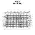
- FIG. 30 shows the schematic structure of an surface discharge AC plasma display panel (PDP) 10P in the prior art.
- PDP surface discharge AC plasma display panel
- electrodes X1 to X5 are formed parallel to one another at equal pitch and electrodes Y1 to Y5 are formed parallel to one another to form parallel pairs with the corresponding electrodes X1 to X5.
- address electrodes A1 to A6 are formed in the direction that runs at a right angle to the aforementioned electrodes, and phosphor covers on that.
- partitioning walls 171 to 177 and partitioning walls 191 to 196 are arranged intersecting each other in a lattice, to ensure that no erroneous display is made through discharge of one pixel affecting adjacent pixels.
- the surface discharge PDPs have an advantage in that the phosphor do not become degraded due to the impact of ions on it since discharge occurs between adjacent electrodes on the same surface.
- a pair of electrodes is provided for each of the display lines L1 to L5
- the degree to which the pixel pitch can be reduced is limited and this is a stumbling block for achieving high definition.
- the scale of the drive circuit must be large since there is a high number of el ectrodes.
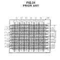
- partitioning walls 191 to 199 are provided on the central lines of the electrodes X1 to X5 and Y1 to Y4, which are surface discharge electrodes, and these electrodes, except for the electrodes X1 and X5 at the two sides, i.e., the electrodes X2 to X4 and the electrodes Y1 to Y4, are commonly used by display lines that are adjacent in the direction of the address electrodes.
- the number of electrodes is almost halved and the pixel pitch can be reduced, achieving higher definition compared to the PDP shown in FIG. 30.
- the scale of the drive circuit can also be halved.
- the distance between the electrodes at the two sides of each of the partitioning walls 191 to 196 must be increased in the structure shown in FIG. 30, so as to reduce the effect of their electric fields between that electrodes. Consequently, the pixel pitch increases, preventing achievement of higher definition.
- the distance between the electrodes Y1 and X2 (non display line) is 300 ⁇ m when the distance between the electrodes Y1 and X2 (display line) is 50 ⁇ m.
- the color of the phosphor is white or bright gray, incident light from the outside is reflected on the phosphor at non display line when observing an image on the PDP in bright place, lowering the contrast of the image.
- a method of driving a plasma display panel having a substrate, a plurality of X-electrodes formed at said substrate, a plurality of Y-electrodes formed at said substrate and a plurality of address electrodes formed at said substrate or at another substrate facing said substrate, each Y-electrode being arranged between two X-electrodes, and said address electrodes crossing the X-electrodes and the Y-electrodes, the method comprising the steps of, for each of the Y-electrodes:
- the display lines in alternate fields or frames can be made so as not to affect each other in regard to discharge, it is not necessary to provide partitioning walls along the central lines on the electrodes X1 to Xn+1 and electrodes Y1 to Yn of the plasma display panel.
- partitioning walls along the central lines on the electrodes X1 to Xn+1 and electrodes Y1 to Yn of the plasma display panel are not necessary.
- a plasma display apparatus comprising:
- the first sustaining means may be arranged to supply alternatively a first sustaining potential pulse and a second sustaining potential pulse, whereby the first sustaining potential pulse is supplied to the Y-electrodes with odd numbers and the X-electrodes with even numbers, and the second sustaining potential pulse is supplied to the Y-electrodes with even numbers and the X-electrodes with odd numbers; and the second sustaining means may be arranged to supply alternatively a first sustaining potential pulse and a second sustaining potential pulse, whereby the first sustaining potential pulse is supplied to the Y-electrodes with odd numbers and the X-electrodes with odd numbers, and the second sustaining potential pulse is supplied to the Y-electrodes with even numbers and the X-electrodes with even numbers.
- the first sustaining means may supply the first and second AC sustaining pulses with ensuring that voltage waveforms applied to the electrodes Yo and Xe are of the same phase to each other, that voltage waveforms applied to the electrodes Ye and Xo are of the same phase to each other and that the first and second AC sustaining pulses are of the reverse phase to each other; and the second sustaining means may supply the third and fourth AC sustaining pulses with ensuring that voltage waveforms applied to the electrodes Yo and Xo are of the same phase to each other, that voltage waveforms applied to the electrodes Ye and Xe are of the same phase to each other and that the third and fourth AC sustaining pulses are of the reverse phase to each other.
- the first addressing means in a first period, may apply a DC voltage to all odd-numbered electrodes among the electrodes X1 to Xn+1 and may apply a pulse with a reverse polarity voltage against the DC voltage to the electrode Yo, and in a second period, may apply the DC voltage to all even-numbered electrodes among the electrodes X1 to Xn+1 and may apply a pulse with a reverse polarity voltage against the DC voltage to the electrode Ye; and the second addressing means, in a third period, may apply the DC voltage to all the even-numbered electrodes among the electrodes X1 to Xn+1 and may apply a pulse with a reverse polarity voltage against the DC voltage to the electrode Yo, and in a fourth period, may apply the DC voltage to all the odd-numbered electrodes among the electrodes X1 to Xn+1 and may apply a pulse with a reverse polarity voltage against the DC voltage to the electrode Ye.
- the first addressing means may apply pulses with reverse polarity voltages to each other to the electrodes Yi and Xi when causing the discharge to occur between the electrode Yi and the electrode Xi; and the second addressing means may apply pulses with reverse polarity voltages to each other to the electrodes Yi and Xi+1 when causing the discharge to occur between the electrode Yi and the electrode Xi+1.
- the first and second addressing means may include : a first sustain circuit for outputting a first voltage-waveform of a DC pulse train; a second sustain circuit for outputting a second voltage-waveform with its phase offset by 180° from a phase of the first voltage-waveform; a switching circuit having switching elements for selectively supplying either the first or second voltage-waveform to the electrodes Yo, Ye, Xo and Xe; and a control circuit for controlling the switching elements of the switching circuit in such a way that the first voltage-waveform is supplied to the electrodes Yo and Xe and the second voltage-waveform is supplied to the electrodes Ye and Xo after the first wall charge having been generated and that the first voltage-waveform is supplied to the electrodes Yo and Xo and the second voltage-waveform is supplied to the electrodes Ye and Xe after the second wall charge having been generated.
- Each of the electrodes X1 to Xn+1 and Y1 to Yn may include a transparent electrode formed at the substrate, and a metal electrode formed at the transparent electrode with a width smaller that the transparent electrode. In this way, the structure of each display line may be made identical.
- the first sustaining means may be arranged to supply alternatively a first sustaining potential pulse and a second sustaining potential pulse, whereby the first sustaining potential pulse is supplied to the Y-electrodes and the second sustaining potential pulse is supplied to the X-electrodes with odd numbers; and the second sustaining means may be arranged to supply alternatively a first sustaining potential pulse and a second sustaining potential pulse, whereby the first sustaining potential pulse is supplied to the Y-electrodes and the second sustaining potential pulse is supplied to the X-electrodes with even numbers.
- the pixel pitch can be reduced compared to the prior art structure in which two display lines are formed with four parallel electrodes, making it possible to achieve higher definition.
- the structure is simplified.
- the address period can be reduced by half compared to that with non-interlaced scanning, lengthening the period of sustaining discharge. This makes it possible to achieve a higher number of gradations by increasing the number of sub frames or makes it possible to achieve higher brightness by increasing the number of times sustaining discharge is performed.
- the electrodes Xo, Yi and Xe may have substantially symmetrical forms relative to a central line of the electrode Yi; each of the electrodes may have a transparent electrode formed at the substrate, and a metal electrode formed at the transparent electrode at a width smaller than that of the transparent electrode; and the metal electrodes of the electrodes Xo and Xe may be arranged on sides away from the electrode Yi .
- the pixel area can be increased compared to a case in which the metal electrode is formed along the central line on the transparent electrode, even if the electrode pitch is reduced to achieve higher definition.
- the sides of the electrodes Xo and Xe, which are opposite to the electrode Yi, are non-display lines, and as the non display lines can be narrowed , this can be desirable.
- the electrodes Xo, Yi and Xe may have substantially symmetrical forms relative to a central line of the electrode Yi; the electrode Yi may be a metal electrode formed at the substrate; each of the electrode Xo and the electrode Xe may have a transparent electrode formed at the substrate, and a metal electrode formed at the transparent electrode at a width smaller than that of the transparent electrode; and the metal electrodes of the electrodes Xo and Xe may be arranged on sides away from the electrode Yi.
- a plasma display panel a method of driving same and a plasma display apparatus, which achieve higher quality image, more especially a higher definition by reducing pixel pitch.
- Further preferred embodiments can provide a plasma display panel, a method of driving the same and a plasma display apparatus that can increase black display quality reduced by whole-screen (all pixel) discharge light emission during a reset period.
- Still further preferred embodiments can provide a plasma display panel, a method of driving the same and a plasma display apparatus that can increase image contrast by decreasing the reflected light from a non-display line.
- Yet further preferred embodiments can provide a plasma display panel, a method of driving the same and a plasma display apparatus that can increase the number of gradations and brightness by addressing a plurality of display lines simultaneously to decrease the address period
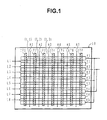
- FIG. 1 shows a PDP 10 in the first embodiment according to the present invention .
- pixels are indicated with dotted lines only for display line L1.
- the present invention may be applied to both color and monochromatic pixels and three monochromatic pixels corresponds to one color pixel.
- the PDP 10 has a structure in which the partitioning walls 191 to 199 in the PDP 10Q in FIG. 31 are removed .
- interlaced scanning is performed in such a manner that the phases of the waveforms of the sustaining pulse voltages in the odd-numbered lines and in the even-numbered lines among the electrodes L1 to L8, which perform surface discharge and will be explained later, are reversed from each other (in the prior art interlaced scanning, since lines L2, L4, L6 and L8 are non-display lines, lines L1 and L5 are scanned in odd-numbered fields and the lines L3 and L7 are scanned in even-numbered fields).
- FIG. 2 shows a state in which the distance between the opposite surfaces of a color pixel 10A is expanded.
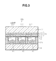
- FIG. 3 shows a longitudinal cross section of the color pixel 10A along an electrode X1.
- transparent electrodes 121 and 122 On one surface of a glass substrate 11 as a transparent substrate of insulator, transparent electrodes 121 and 122, constituted with IT0 film or the like, are provided parallel to each other and, in order to minimize the reduction in voltage in the transparent electrodes 121 and 122 along the lengthwise direction, metal electrodes 131 and 132, constituted with copper or the like, are formed along the central lines of the transparent electrodes 121 and 122 respectively.
- the transparent electrode 121 and the metal electrode 131 constitute the electrode X1 and the transparent electrode 122 and the metal electrode 132 constitute an electrode Y1.
- a dielectric substance 14 for holding the wall charge covers the glass substrate 11 and the electrodes X1 and Y1.
- the dielectric substance 14 is covered with an MgO protective film 15.
- address electrodes A1, A2 and A3 are formed in the direction which runs at a right angle to the electrodes X1 and Y1, with partitioning walls 171 to 173 partitioning them.
- the discharge space between the phosphors 181 to 183 and the MgO protective film 15 is filled with Ne + Xe Penning mixed gas, for instance.
- the partitioning walls 171 to 174 prevent the ultraviolet light generated during a discharge from entering adjacent pixels and also function as spacers for forming the discharge space. If the phosphors 181 to 183 are constituted with an identical substance, the PDP 10 will be a monochromatic display.
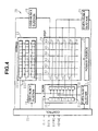
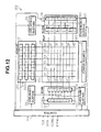
- FIG. 4 shows the schematic structure of a plasma display apparatus 20 which employs the PDP 10 structured as described above.
- a control circuit 21 converts the display data DATA supplied from the outside to data for the PDP 10, supplies them to a shift register 221 of an address circuit 22 and, based upon a clock signal CLK, a vertical synchronization signal VSYNC and a horizontal synchronization signal HSYNC provided from the outside, generates various control signals which are provided to components 22 to 27.
- voltages Vaw, Va and Ve are supplied to the address circuit 22 and voltages -Vc, -Vy and Vs are supplied to an odd-numbered Y sustain circuit 24 and an even-numbered Y sustain circuit 25, and voltages Vw, Vx and Vs are supplied to an odd-numbered X sustain circuit 26 and an even-numbered X sustain circuit 27, from a power source circuit (power supply circuit) 29.
- bits 221 (1) to 221 (6) are held in bits 222 (1) to 222 (6) respectively of a latch circuit 222, and in correspondence to their values, switching elements (not shown) inside drivers 223 (1) to 223 (6) are ON/OFF controlled and a binary voltage pattern whereby the voltage is either Va or 0V is supplied to the address electrodes A1 to A6.
- a scanning circuit 23 is provided with shift registers 231 and drivers 232. During an address period, "1" is supplied to a serial data input of the shift registers 231 for the initial address cycle only in each VSYNC cycle and then it is shifted in synchronization with the address cycle. ON/OFF control is performed for switching elements (not shown) in the drivers 232 (1) to 232 ( 6) with the values of the bits 231(1) to 231(4) in the shift register 231 and the selected voltage -Vy or the unselected voltage -Vc is applied to the electrodes Y1 to Y4.
- the electrodes Y1 to Y4 are sequentially selected by the shifting operation of the shift register 231 and the selected voltage -Vy is applied to the selected electrodes Y and the unselected voltage -Vc is applied to the electrodes Y which have not been selected.
- These voltages -Vy and -Vc are supplied from the odd-numbered Y sustain circuit 24 and the even-numbered Y sustain circuit 25.
- a first sustaining pulse train is supplied from the odd-numbered Y sustain circuit 24 to the odd-numbered electrodes Y1 and Y3 of the Y electrodes via the drivers 232 (1) and 232 (3) and a second sustaining pulse train whose phase is shifted by 180 from the that of first sustain pulse train is supplied from the even-numbered Y sustain circuit 25 to the even-numbered electrodes Y2 and Y4 of the Y electrodes via the drivers 232(2) and 232(4).
- the second sustaining pulse train is supplied from the odd-numbered X sustain circuit 26 to the odd-numbered electrodes X1, X3 and X5 of the X electrodes and the first sustaining pulse train is supplied from the even-numbered X sustain circuit 27 to the even-numbered electrodes X2 and X4 of the X electrodes.
- a whole-screen (all pixel) write pulse is commonly supplied to the electrodes X1 to X5 from the X sustain circuits 26 and 27 respectively.
- a pulse train for two address cycles is supplied to the odd-numbered electrodes X1, X3 and X5 of the X electrodes from the odd-numbered X sustain circuit 26, and a pulse train whose phase is shifted by 180° from the aforementioned pulse train, is supplied to the even-numbered electrodes X2 and X4 of the X electrodes from the even-numbered X sustain circuit 27.
- circuits 223, 232, 24, 25, 26 and 27 are switching circuits for switching on/off voltages supplied from a power source circuit 29.
- FIG. 5 shows the structure of one frame of the display image.
- This frame is divided into two fields, i.e., an even-numbered field and an odd-numbered field and each field consists of first to third subfields.
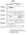
- voltages with the waveforms shown in FIG. 7 are supplied to the various electrodes of the PDP 10 in odd-numbered field to display lines L1, L3, L5 and L7 shown in FIG. 1, and voltages with the waveforms shown in FIG. 8 are supplied to the various electrodes of the PDP 10 in the even-numbered field to display lines L2, L4, L6 and L8 shown in FIG. 1 .
- the sustaining periods in the first to third subfields are T1, 2T1 and 4T1 respectively and in each subfield, sustaining discharge is performed a number of times that corresponds to the length of the sustaining period.
- the brightness will have eight gradations.
- the brightness will have 256 gradations.
- the scanning of the display lines during an address period is perfcrmed in the order of the numbers assigned inside the circles in FIG. 6(A). Namely, for the odd-numbered field, scanning is performed in the order of the display lines L1, L3, L5 and L7 and for the even-numbered field, scanning is performed in the order of the display lines L2, L4, L6 and L8.
- W, E, A and S in FIG. 7 respectively indicate time points at which whole-screen write discharge, whole-screen self-erasing discharge, address discharge and sustaining discharge occur.
- W, E, A and S in FIG. 7 respectively indicate time points at which whole-screen write discharge, whole-screen self-erasing discharge, address discharge and sustaining discharge occur.
- the areas between address electrodes and Y electrodes are referred to as the areas between A-Y electrodes and this reference system applies to the areas between other electrodes.
- the waveforms of the voltages supplied to the X electrodes, which are whole-screen write pulses, are identical to one another
- the waveforms of the voltages supplied to the Y electrodes are identical to one another at 0V
- the waveforms of the voltages supplied to the address electrodes, which are intermediate voltage pulses are identical to one another.
- the voltage applied to each electrode is set at 0V. Because of the last sustaining pulse of the sustain period before the reset period, positive wall charges are present on the MgO protective film 15 near the X electrodes (on the X-electrode sides) and negative wall charges are present on the MgO protective film 15 near the Y electrodes (on the Y-electrode sides), for the pixels that are lit . Hardly any wall charge is present on the X-electrode sides or the Y-electrode sides for the pixels that are not lit .
- a reset pulse at the voltage Vw is supplied to the X electrodes and an intermediate voltage pulse at the voltage Vaw is supplied to the address electrodes.
- Vw 310V and Vw > Vfxy.
- whole-screen write discharge W is generated between adjacent X-Y electrodes, i.e., between the X-Y electrodes for the display lines L1 to L8.
- the resulting electrons and positive ions are attracted by the electric fields caused by the voltage Vw between the X-Y electrodes to generate a wall charge of reverse polarity. This reduces the strength of the electric field in the discharge space to terminate the discharge in 1 to several ⁇ s.
- the voltage Vaw is approximately Vw/2 and since the absolute values of the voltage between the A-X electrodes and the voltage between the A-Y electrodes, whose phases are reversed from each other, are almost equal to each other, the average wall charge remaining in the phosphors due to the discharge is approximately 0.
- the waveforms of the voltages supplied to the odd-numbered X electrodes are identical to one another, the waveforms of the voltages supplied to the even-numbered X electrodes are identical to one another, and the waveforms of the voltages supplied to the unselected Y electrodes are identical to one another with the voltage at -Vc.
- a scanning pulse at the voltage -Vy is supplied to the electrode Y1 and a write pulse at the voltage Va is supplied to each of the address electrodes for the pixels that are to be lit.
- Va + Vy > Vfay is satisfied and address discharge only occurs for the pixels to be lit, and the discharge ends by a generated wall-charge with a reverse polarity.
- a pulse at voltage Vx is supplied only to the electrode X1 of the electrodes X1 and X2 which are adjacent to the electrode Y1.
- Vxyt the discharge start voltage between the X-Y electrodes, triggered by this address discharge, is designated Vxyt
- Vx + Vc ⁇ Vxyt ⁇ Vx + Vy ⁇ Vfxy is satisfied and a write discharge occurs between the X1-Y1 electrodes in the display line L1.
- a scanning pulse at the voltage -Vy is supplied to the electrode Y2
- a pulse at the voltage Vx is supplied to the even-numbered X electrodes
- a write pulse at the voltage Va is supplied to the address electrodes for the pixels to be lit.
- a write discharge of display data occurs for the pixels to be lit in the order of the display lines L1, L3, L5 and L7, a positive wall charge is generated on the Y-electrode sides and a negative wall charge is generated on the X-electrode sides.
- a sustaining pulse with the same phase and at the same voltage Vs is cyclically, or the first sustaining pulse train is supplied to the odd-numbered X electrodes and the even-numbered Y electrodes, and a second sustaining pulse train which is generated by shifting the phase of the first sustaining pulse train by 180° (1/2 cycle) is supplied to both the even-numbered X electrodes and the odd-numbered Y electrodes.
- the voltage Ve is supplied to the address electrodes, which are sustained until the sustain period ends.
- a sustaining pulse at the voltage Vs is supplied to the odd-numbered Y electrodes and the even-numbered X el ectrodes.
- the effective voltage of a pixel between the odd-numbered Y electrode and the odd-numbered X electrode is Vs + Vwall
- the effective voltage of a pixel between the even-numbered Y electrode and the even-numbered X electrode is Vs - Vwall
- the effective voltages of a pixel between the odd-numbered X electrode and the even-numbered Y electrode and a pixel between the even-numbered X electrode and the odd-numbered Y electrode are 2Vwall.
- Vs ⁇ Vfxy ⁇ Vs + Vwall, 2Vwall ⁇ Vfxy are satisfied, a sustaining discharge occurs between the odd-numbered Y electrodes and the odd-numbered X electrodes and a wall charge with reverse polarity is generated to end the discharge. Sustaining discharge does not occur between other electrodes. As a result, display is effective only in the odd-numbered display lines L1 and L5 within the odd-numbered field. Only this time, the sustaining discharge between the even-numbered Y electrodes and the even-numbered X electrodes does not occur.
- a sustaining pulse at the voltage Vs is supplied to the odd-numbered X electrodes and the even-numbered Y electrodes.
- the effective voltages of a pixel between the odd-numbered X electrode and the odd-numbered Y electrode and a pixel between the even-numbered Y electrode and the even-numbered X electrode are both Vs + Vwall whereas the effective voltages of a pixel between the odd-numbered Y electrode and the even-numbered X electrode and a pixel between the odd-numbered X electrode and the even-numbered Y electrode are zero.
- the sustaining discharge is repeated in the manner described above.
- the effective voltages of a pixel between the odd-numbered Y electrode and the even-numbered X electrode and a pixel between the odd-numbered X electrode and the even-numbered Y electrode in the undisplayed lines are zero.
- the last sustaining discharge during the sustain period is performed in such a manner that the polarity of the wall charge is in the initial state during the reset period described earlier.
- the display of the display lines L1, L3, L5 and L7 which are constituted with pairs of electrodes, the electrodes Y1 to Y4 and the electrodes X1 to X4 that are adjacent to the electrodes Y1 to Y4 toward the upper side in FIG. 1, are effective in the odd-numbered field, as explained above.
- the display of the display lines L2, L4, L6 and L8 which are constituted with the electrodes Y1 to Y4 and the electrodes X2 to X5 that are adjacent to the electrodes Y1 to Y4 toward the lower side in FIG. 1, must be made effective.
- FIG. 8 shows the waveforms of the voltages applied to those electrodes in the even-numbered field.
- the PDP can be structured as shown in FIG . 1 by removing the partitioning walls 191 to 199 in the PDP 10Q in FIG. 31, facilitating the production of the PDP 10 with reduced production cost and achieving higher definition by reducing the pixel pitch.
- the number of pulses can be reduced in FIGs. 7 and 8, power consumption can also be reduced.
- the pulses supplied to the odd-numbered X electrodes and the even-numbered X electrodes are made to be continuous, the number of pulses can be reduced. This can be achieved by performing scanning in the order shown in FIG. 6(B).
- the display lines L1, L3, L5 and L7 in the odd-numbered field should be further divided into odd-numbered lines and even-numbered lines and after scanning one group sequentially, the other group should be scanned sequentially. The same procedure is performed for the even-numbered field.
- FIG. 9 shows the schematic structure of a plasma display apparatus 20A in the second embodiment for implementing this method.
- a scanning circuit 23A differs from the scanning circuit 23 shown in FIG. 4 in that the output of an odd-numbered Y sustain circuit 24 is connected to the inputs of the driver 232 (1) and the driver 232 (2) and the output of an even-numbered Y sustain circuit 25 is connected to the inputs of the driver 232 (3) and the driver 232 (4).
- an odd-numbered X sustain circuit 26A and an even-numbered X sustain circuit 27A output signals to ensure that the waveforms of the voltages applied to the odd-numbered X electrodes and the even-numbered X electrodes are as shown in FIGS. 10 and 11.
- each of the odd-numbered X electrodes and the even-numbered X electrodes require only one pulse with a large width to be supplied during each address period of the odd-numbered field or the even-numbered field, resulting in a reduction in power consumption compared to the structure shown in FIG . 4 .
- the structures of the odd-numbered X sustain circuit 26A and the even-numbered X sustain circuit 27A are simplified compared to those of the odd-numbered X sustain circuit 26 and the even-numbered X sustain circuit 27 shown in FIG. 4.
- the common pulse at the voltage Vx is supplied to the electrodes X1, X3 and X5 and the common pulse at the voltage Vx is supplied to the electrodes X2 and X4.
- a scanning circuit 30 is provided for the X electrodes, too, as shown in FIG. 12.
- the scanning circuit 30 is different from the scanning circuit 23 only in that the number of components is larger by the equivalent of one electrode.
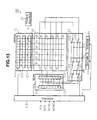
- a plasma display apparatus 20C is structured as shown in FIG . 13.
- the odd-numbered Y sustain circuit 24, the even-numbered Y sustain circuit 25, the odd-numbered X sustain circuit 26 and the even-numbered X sustain circuit 27 in FIG. 4 are replaced by sustain circuits 31 and 32 and a switching circuit 33 .
- the waveforms S1 and S2 of the output voltages from the sustain circuits 31 and 32 are identical to the waveforms of the voltages applied to the odd-numbered X electrodes and the even-numbered X electrodes shown in FIG. 7.
- FIG. 13 the odd-numbered Y sustain circuit 24, the even-numbered Y sustain circuit 25, the odd-numbered X sustain circuit 26 and the even-numbered X sustain circuit 27 in FIG. 4 are replaced by sustain circuits 31 and 32 and a switching circuit 33 .
- the switching circuit 33 is provided with changeover switching elements 331 and 332 which interlock with each other, changeover switching elements 333 and 334 that interlock with each other and changeover switching elements 335 and 336 which interlock with each other.
- changeover switching elements may be constituted with FETs, for instance.
- the switching control for the switching circuit 33 is executed by a control circuit 21B.
- the changeover switching elements 331 and 332 are switched over from the state shown in FIG. 13, the voltage waveforms S2 and S1 are supplied to the inputs of the odd-numbered elements of the driver 232 and the even-numbered elements of the driver 232 respectively and this corresponds to the sustain period shown in FIG . 7.
- the changeover switching elements 335 and 336 are switched over in this state, the voltage waveforms S2 and S1 are supplied to the odd-numbered X electrodes and the even-numbered X electrodes and this corresponds to the sustain period shown in FIG. 8.
- the same operation as that performed by the unit shown in FIG. 4 can be performed in a simpler structure compared to the unit shown in FIG . 4.
- FIG. 15 shows a plasma display apparatus 20D in which these features are adopted as a fifth embodiment according to the present invention.
- the sustain circuits 31 and 32 and the switching circuit 33 perform operation identical to that performed in FIG. 13, based upon control signals from a control circuit 21C.
- the first subfield in FIG. 16 is the same as that in FIG . 7 and during a reset period, light emission due to the whole-screen write discharge W and the whole-screen self-erasing discharge E occurs for the undisplayed lines, too. This is necessitated because the wall charge performed in the preceding even-numbered field must be eliminated. However, since no discharge occurs in undisplayed lines during an address period and a sustain period, it is not necessary to cause a write discharge W and a self-erasing discharge E in the undisplayed lines during the reset period in the second and subsequent subfields of an odd-numbered field.
- a pulse at the voltage Vaw is supplied to the address electrodes in correspondence to the write voltage supplied to odd-numbered X electrodes and the even-numbered X electrodes.
- the reset period in the third or subsequent subfields of the odd-numbered field is also the same as the reset period of the second subfield.
- FIG. 18 shows a plasma display apparatus 20E in the seventh embodiment according to the present invention.
- the schematic structure of the PDP 10A is identical to that of the PDP 10 shown in FIG . 1.
- the electrodes are used differently from that shown in FIG . 4. Namely, the electrodes Y1, Y2 and Y3 are not divided into odd-numbered and even-numbered groups but the electrodes X1, X3 and X5 which are adjacent to the electrodes Y1 to Y3 on one side are designated the odd-numbered X electrodes and the electrodes X2, X4 and X6 which are adjacent to the electrodes Y1 to Y3 on the other side are designated the even-numbered X electrodes.
- Interlaced display is executed for odd-numbered display lines constituted with pairs of electrodes (Y1, X1), (Y2, X3) and (Y3, X5) and even-numbered display lines constituted with pairs of electrodes (Y1, X2), (Y2, X4) and (Y3, X6).
- the lines between the even-numbered X electrode and the odd-numbered X electrode are completely undisplayed lines.
- the pixel pitch can be shortened compared to the structure, as shown in FIG. 30, in which two display lines are formed with four parallel electrodes and partitioning walls parallel to the electrodes for surface discharge are provided, making higher definition possible.
- the electrodes Y1 to Y3 are not divided into an even-numbered group and an odd-numbered group, the structure is simplified compared to that in the first embodiment.
- FIG. 19 shows a longitudinal cross section of the PDP 10A shown in FIG . 18 along the address electrodes.
- the difference of this structure from the structure shown in FIG. 2 is that for the electrodes X1 and X2 at the two sides of the electrode Y1, metal electrodes 131 and 133 are formed toward the side which is furthest away from the electrode Y1 on transparent electrodes 121 and 123 respectively.
- This structural feature is adopted at the two sides of each of the Y electrodes. This makes the electric field stronger on the metal electrode 131 side above the electrode X1 when a voltage is supplied between the X1-Y1 electrodes and, therefore, even if the electrode pitch is reduced in order to achieve higher definition, the pixel area can be increased compared to the structure in which the metal electrode 131 is formed along the central line on the transparent electrode 121.
- the lines on the opposite sides of the electrodes X1 and X2 relative to the electrode Y1 are undisplayed lines, this is feasible and, moreover, it is desirable because the undisplayed lines can be narrowed.
- the width of the transparent electrode 122 is made equal to the widths of the transparent electrodes 121 and 123, the width of the electrode Y1, which is supplied with the scanning pulse, may be narrow to reduce the power consumption.
- a scanning circuit 23B, an odd-numbered sustain circuit 26B and an even-numbered sustain circuit 27B respectively correspond to the scanning circuit 23, the odd-numbered X sustain circuit 26 and the even-numbered X sustain circuit 27 shown in FIG. 4.
- a single Y sustain circuit 24A can replace the odd-numbered Y sustain circuit 24 and the even-numbered Y sustain circuit 25, simplifying the structure.
- FIG. 20 shows the order in which the display lines are scanned during an address period. Since the lines between the even-numbered X electrode and the odd-numbered X electrode is completely undisplayed line, if one frame is to be divided into an odd-numbered field and an even-numbered field as shown in FIG . 6 6(A), the display lines will be thinned out at the ratio of one to three in each field, which is not desirable from the viewpoint of maintaining display quality.
- This problem is solved by scanning the display lines L1, L3 and L5 sequentially with only writing the display data of the odd-numbered field at the odd-numbered frame, and by scanning the display lines L2, L4 and L6 sequentially with only writing the display data of the even-numbered field at the even-numbered frame.
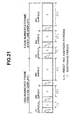
- the structure of the frame corresponding to that in FIG . 5 is as shown in FIG . 21.
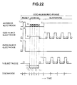
- FIG. 22 shows the waveforms of the voltages applied to the electrodes in the odd-numbered frame in case that a number of Y electrodes is four.
- a sustain pulse at the voltage Vs is cyclically supplied to the Y electrodes, a pulse train obtained by shifting the phase of the pulse train to the Y el ectrodes by 180° is supplied to the odd-numbered X electrodes.
- an AC sustain pulse is supplied between the odd-numbered X electrode and the Y electrode and sustaining discharge occurs in the same manner as that in the first embodiment. Since the even-numbered X electrodes are set at 0V, AC voltage is not supplied to the undisplayed lines between the even-numbered X electrode and the Y electrode and the even-numbered X electrode and the odd-numbered X electrode and, therefore, discharge does not occur among these electrodes.
- FIG. 23 shows the waveforms of the voltages supplied to the electrodes in the even-numbered frame. These waveforms are obtained by reversing the waveforms of the voltages supplied to the odd-numbered X electrodes and the even-numbered X electrodes to each other in FIG . 22.
- the address period is reduced by half compared to that with non interlaced scanning, the sustaining discharge period is lengthened. With this, it becomes possible to achieve a higher number of gradations by increasing the number of sub frames or it becomes possible to achieve higher brightness by increasing the number of times the sustaining discharge is performed.
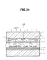
- FIG. 24 shows the longitudinal cross section of part of the PDP 10B in the eighth embodiment according to the present invention, along the address electrodes.
- the transparent electrode 122 is omitted by constituting the electrode Y1 only with the metal electrode 132. This also applies to all the other Y electrodes. With this, as described earlier, the power consumption is reduced when scanning pulses are supplied to the Y electrodes. Moreover, it is possible to further reduce the pixel pitch.
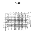
- a PDP 10C as shown in FIG. 25, is employed to reduce the unwanted light emission.
- alternate lines between electrodes in the PDP 10 in FIG. 1 are blind lines B1 to B3. Since the blind lines B1 to B3 are undisplayed lines, non-interlaced scanning is performed for the display lines L1 to L4.
- Blind films ( light-blocking masks) 41 to 43 are formed, for instance, at the portion between the transparent electrodes 121 and the transparent electrode 122 in FIG . 2 or on the surface of the glass substrate 11 which corresponds to this portion to ensure that the unwanted light emission at the blind lines B1 to B3 will not leak toward the viewer.
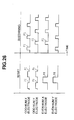
- FIG. 26 shows the waveforms of the voltages applied to the electrodes during a reset period and during a sustain period, and an address period is omitted.
- PE indicates an erasing pulse
- PW indicates a write pulse
- PS indicates a sustaining pulse.
- an erasing pulse PE whose voltage is lower than that of the sustaining pulse is supplied to the odd-numbered X electrodes and the odd-numbered Y electrodes, to perform erasing discharge for the wall charge at all the blind lines B1 to B3.
- write pulse PW whose voltage is higher than that of the sustaining pulse is supplied to the even-numbered X electrodes and the even-numbered Y electrodes, to perform write discharge at all the blind lines B1 to B3, and the wall charge becomes almost constant at all the blind lines B1 to B3 .
- the voltage of the write pulse PW is equal to or higher than the discharge start voltage but is lower than the voltage Vw in FIG.
- the erasing pulse PE is supplied to the odd-numbered X electrodes and the odd-numbered Y electrodes again, to perform erasing discharge for the wall charge at all the blind lines B1 to B3 .
- any floating space charge that has not been reunited flows into the display lines L1 to L4, making the address discharge occur more easily during an address period.
- discharge is not performed and the quali ty of black display areas is prevented from becoming degraded due to the generation of unwanted light emission.
- the waveforms of the voltages applied to the electrodes during the address period are identical to those in the prior art for the display lines L1 to L4 or identical to those when the odd-numbered field in FIG. 7 is regarded as one frame.
- the sustain period is identical to that in the case shown in FIG . 7.
- the PDP is of a driving type which does not discharge at the blind lines B1 to B3, by making an observer-side surface of the blind films 41 to 43 darker than the phosphor, preferably black, in order to absorbs incident light to the blind lines B1 to B3 from the outside, the contrast of an image on the PDP in bright place increases more than a case that incident light to the phosphor at the blind lines B1 to B3 from the outside is reflected and enters eyes of an observer.
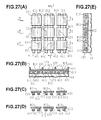
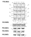
- FIGs. 27 (A) to 27 (E) show the address electrodes in the 10th embodiment according to the present invention.
- FIG . 27 (A) is a plan view and FIGS. 27 (B) to 27(E) are cross sections along lines B-B, C-C, D-D, and E-E respectively in FIG. 27 27(A).
- FIGS. 28 (B) and 28(E) the structure surrounding the address electrodes is also shown, which facilitates understanding of the structures of other portions in relation to FIG. 2.
- a pair of address electrodes A11 and A21 are formed on a glass substrate 16.
- pads B11, B21 and B31 are formed in correspondence to the individual monochromatic pixels.
- the address electrode All is connected to the pad B21 via a contact C21 and the address electrode A21 is connected to the pad B11 and B31 via contacts C11 and C31 respectively.
- the pads that are arrayed in one row are connected alternately to the address electrode All and the address electrode A21.
- a given odd-numbered line and a given even-numbered line i.e., the line constituted with the pads B11 to B13 and the line constituted with the pads B21 to B23, for instance, can be selected at the same time, an address pulse for the line constituted of the pads B21 to B23 can be supplied to the address electrodes All to A13 and at the same time, an address pulse for the line constituted with the pads B11 to B13 can be supplied to the address electrodes A21 to A23.
- the address period is reduced by half compared to that in the prior art .
- the sustaining discharge period is increased. With this, it is possible to increase the number of sub frames to achieve a higher number of gradations or to increase the number of times sustaining discharge is performed and achieve higher brightness.
- the tenth embodiment according to the present invention may be adopted in various types of PDPs.
- FIG. 28 shows the address electrodes in the eleventh embodiment according to the present invention.
- FIG. 28 (A) is a plan view and FIGS. 28 (B) to 28 (E) are cross sections along lines B-B, C-C, D-D, and E-E in FIG. 28 (A) respectively.
- FIG. 28 (B) also shows the structure of the surrounding area of the address electrodes.
- address electrodes are formed in each area between partitioning walls and above the address electrodes, pads are formed inside the phosphors, with one column of pads connected sequentially to four electrode lines.
- reference characters A11 to A43 indicate address electrodes
- reference characters B11 to B43 indicate pads
- reference characters C11 to C43 indicate contacts.
- any two odd-numbered lines and any two even-numbered lines can be selected at the same time for supplying an address pulse.
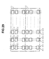
- FIG. 29 shows the schematic structure of the address electrodes in the twelfth embodiment according to the present invention.
- the display surface is divided into two portions, i.e., an area 51 and an area 52, with the address electrode All connected to pads in the area 51 and the address electrode A21 connected to pads in the area 52. The same applies to all the other address electrodes and pads.
- any display line in the area 51 and any display line in the area 52 can be selected at the same time for supplying an address pulse.
- the address electrodes and the X electrodes and the Y electrodes are formed at glass substrates that face each other across the discharge space
- the present invention may be applied in a structure in which they are all formed on the same glass substrate.
- the present invention may be applied in a structure in which whole-screen write is performed for the wall charge during a reset period and the wall charge is erased for the pixels to be turned off during an address period.
- the metal electrode 131 may be formed on the reverse surface or both surfaces of the transparent electrode 121 or in the transparent electrode 121. The same applies to all the other metal electrodes in FIGS. 1, 19 and 24.
Landscapes
- Engineering & Computer Science (AREA)
- Physics & Mathematics (AREA)
- Plasma & Fusion (AREA)
- Theoretical Computer Science (AREA)
- Computer Hardware Design (AREA)
- General Physics & Mathematics (AREA)
- Power Engineering (AREA)
- Chemical & Material Sciences (AREA)
- Materials Engineering (AREA)
- Electromagnetism (AREA)
- Control Of Indicators Other Than Cathode Ray Tubes (AREA)
- Control Of Gas Discharge Display Tubes (AREA)
- Gas-Filled Discharge Tubes (AREA)
Claims (22)
- Verfahren zum Antreiben einer Plasmaanzeigetafel, welche Plasmaanzeigetafel ein Substrat (11) hat, eine vielzahl von X-Elektroden (X1 bis Xn+1; X1 bis X2n), die auf dem genannten Substrat gebildet sind, eine Vielzahl von Y-Elektroden (Y1 bis Yn), die auf dem genannten Substrat gebildet sind, und eine Vielzahl von Adreßelektroden, die auf dem genannten Substrat oder auf einem anderen Substrat gebildet sind, das dem genannten Substrat zugewandt ist, wobei jede Y-Elektrode zwischen zwei X-Elektroden angeordnet ist und die Adreßelektroden die X-Elektroden und die Y-Elektroden queren, welches Verfahren die folgenden Schritte für jede der Y-Elektroden umfaßt:(1) Bewirken des Auftretens einer ersten Adreßentladung zwischen der Y-Elektrode und den Adreßelektroden, die in Entsprechung zu Anzeigedaten in einem ersten Feld oder Rahmen selektiert wurden, und Bewirken des Auftretens einer Entladung zwischen der Y-Elektrode und der X-Elektrode, die an die Y-Elektrode auf einer ersten Seite angrenzt, unter Verwendung der ersten Adreßentladung als Trigger, um eine erste Wandladung zu erzeugen, die für eine Halteentladung erforderlich ist, in Entsprechung zu den Anzeigedaten in dem ersten Feld oder Rahmen;(2) Bewirken, nachdem die Wandladung erzeugt worden ist, einer Halteentladung nur zwischen der Y-Elektrode und der X-Elektrode, die an die Y-Elektrode auf der ersten Seite angrenzt, in Entsprechung zu den Anzeigedaten in dem ersten Feld oder Rahmen;(3) Bewirken des Auftretens einer zweiten Adreßentladung zwischen der Y-Elektrode und den Adreßelektroden, die in Entsprechung zu Anzeigedaten in einem zweiten Feld oder Rahmen selektiert wurden, und Bewirken des Auftretens einer Entladung zwischen der Y-Elektrode und der X-Elektrode, die an die Y-Elektrode auf einer zweiten Seite angrenzt, unter-Verwendung der zweiten Adreßentladung als Trigger, um eine zweite Wandladung zu erzeugen, die für eine Halteentladung erforderlich ist, in Entsprechung zu den Anzeigedaten in dem zweiten Feld oder Rahmen; und(4) Bewirken, nachdem die zweite Wandladung erzeugt worden ist, einer Halteentladung nur zwischen der Y-Elektrode und der X-Elektrode, die an die Y-Elektrode auf der zweiten Seite angrenzt, in Entsprechung zu den Anzeigedaten in dem zweiten Feld oder Rahmen.
- Verfahren nach Anspruch 1, bei dem die Vielzahl von Y-Elektroden Elektroden Y1 bis Yn umfaßt und die Vielzahl von X-Elektroden Elektroden X1 bis Xn+1 umfaßt, welche Elektroden X1 bis Xn+1 in numerisch sequentieller Ordnung angeordnet sind, wobei eine Elektrode Yi zwischen einer Elektrode xi und einer Elektrode Xi+1 für jedes i = 1 bis n angeordnet ist.
- Verfahren nach Anspruch 2, bei dem:Schritt (2) das alternative Zuführen eines ersten Haltepotentialimpulses und eines zweiten Haltepotentialimpulses umfaßt, wodurch der erste Haltepotentialimpuls den Y-Elektroden mit ungeradzahligen Nummern und den X-Elektroden mit geradzahligen Nummern zugeführt wird und der zweite Haltepotentialimpuls den Y-Elektroden mit geradzahligen Nummern und den X-Elektroden mit ungeradzahligen Nummern zugeführt wird; undSchritt (4) das alternative Zuführen eines ersten Haltepotentialimpulses und eines zweiten Haltepotentialimpulses umfaßt, wodurch der erste Haltepotentialimpuls den Y-Elektroden mit ungeradzahligen Nummern und den X-Elektroden mit ungeradzahligen Nummern zugeführt wird und der zweite Haltepotentialimpuls den Y-Elektroden mit geradzahligen Nummern und den X-Elektroden mit geradzahligen Nummern zugeführt wird.
- Verfahren nach Anspruch 3, das ferner umfaßt:bei Schritt (2), wenn die ersten und zweiten Halteimpulse zugeführt werden, das Gewährleisten, daß Spannungswellenformen, die auf die Y-Elektroden mit ungeradzahligen Nummern und die X-Elektroden mit geradzahligen Nummern angewendet werden, phasengleich sind, daß Spannungswellenformen, die auf die Y-Elektroden mit geradzahligen Nummern und die X-Elektroden mit ungeradzahligen Nummern angewendet werden, phasengleich sind und daß die ersten und zweiten Halteimpulse gegenphasig zueinander sind; undbei Schritt (4), wenn die ersten und zweiten Halteimpulse zugeführt werden, das Gewährleisten, daß Spannungswellenformen, die auf die Y-Elektroden mit ungeradzahligen Nummern und die X-Elektroden mit ungeradzahligen Nummern angewendet werden, phasengleich sind, daß Spannungswellenformen, die auf die Y-Elektroden mit geradzahligen Nummern und die X-Elektroden mit geradzahligen Nummern angewendet werden, phasengleich sind und daß die ersten und zweiten Halteimpulse gegenphasig zueinander sind.
- Verfahren nach Anspruch 4, das umfaßt:in einer ersten Periode das Anwenden einer Gleichspannung auf alle ungeradzahlig numerierten X-Elektroden und das Anwenden eines Impulses mit entgegengesetzter Polarität zu jener der Gleichspannung auf die ungeradzahlig numerierte Y-Elektrode;in einer zweiten Periode das Anwenden der Gleichspannung auf alle geradzahlig numerierten X-Elektroden und das Anwenden eines Impulses mit entgegengesetzter Polarität zu jener der Gleichspannung auf die geradzahlig numerierte Y-Elektrode;in einer dritten Periode das Anwenden der Gleichspannung auf alle geradzahlig numerierten Elektroden und das Anwenden eines Impulses mit entgegengesetzter Polarität zu jener der Gleichspannung auf die ungeradzahlig numerierte Y-Elektrode; undin einer vierten Periode das Anwenden der Gleichspannung auf alle ungeradzahlig numerierten X-Elektroden und das Anwenden eines Impulses mit entgegengesetzter Polarität zu jener der Gleichspannung auf die geradzahlig numerierte Y-Elektrode.
- Verfahren nach Anspruch 4, das umfaßt:das Anwenden von Impulsen mit zueinander entgegengesetzter Polarität auf die Elektroden Yi und Xi, wenn das Auftreten der Entladung zwischen der Elektrode Yi und der Elektrode Xi bewirkt wird; unddas Anwenden von Impulsen mit zueinander entgegengesetzter Polarität auf die Elektroden Yi und Xi+1, wenn das Auftreten der Entladung zwischen der Elektrode Yi und der Elektrode Xi+1 bewirkt wird.
- Verfahren nach irgendeinem der Ansprüche 4 bis 6, bei dem sowohl das erste Feld als auch das zweite Feld aus einer Vielzahl von Subfeldern mit sich voneinander unterscheidenden Anzahlen von Halteentladungsimpulsen gebildet ist, welches verfahren ferner umfaßt:vor der ersten Adreßentladung in einem ersten Subfeld des ersten Feldes und für i = 1 bis n das Bewirken des Auftretens einer Entladung zwischen der Elektrode Yi und der Elektrode Xi und zwischen der Elektrode Yi und der Elektrode Xi+1, um eine Wandladung bei allen Pixels zu eliminieren oder eine wandladung bei allen Pixels zu erzeugen;vor der ersten Adreßentladung in den anderen Subfeldern des ersten Feldes und für ungeradzahlige Nummern (o) von 1 bis n und für geradzahlige Nummern (e) von 1 bis n das Bewirken des Auftretens einer Entladung D1 zwischen der Elektrode Yo und der Elektrode Xo und des Auftretens einer Entladung D2 zwischen der Elektrode Ye und der Elektrode Xe mit einer Zeitverzögerung gegenüber der Entladung D1, um die Wandladung nur bei Pixels in dem ersten Feld zu eliminieren oder zu erzeugen;vor der zweiten Adreßentladung in einem ersten Subfeld des zweiten Feldes und für i = 1 bis n das Bewirken des Auftretens einer Entladung zwischen der Elektrode Yi und der Elektrode Xi und zwischen der Elektrode Yi und der Elektrode Xi+1, um die Wandladung bei allen Pixels zu eliminieren oder die Wandladung bei allen Pixels zu erzeugen; undvor der zweiten Adreßentladung in den anderen Subfeldern des zweiten Feldes und für ungeradzahlige Nummern (o) von 1 bis n und für geradzahlige Nummern (e) von 1 bis n das Bewirken des Auftretens einer Entladung D3 zwischen der Elektrode Yo und der Elektrode Xo+1 und des Auftretens einer Entladung D4 zwischen der Elektrode Ye und der Elektrode Xe+1 mit einer Zeitverzögerung gegenüber der Entladung D3, um eine Wandladung nur bei Pixels in dem zweiten Feld zu eliminieren oder zu erzeugen.
- Verfahren nach Anspruch 1, bei dem die Vielzahl von Y-Elektroden Elektroden Y1 bis Yn umfaßt und die Vielzahl von X-Elektroden Elektroden X1 bis X2n umfaßt, welche Elektroden Xo, Yi und Xe in numerisch sequentieller Ordnung angeordnet sind, wobei o = 2i-1 ist, e = 2i ist und i = 1 bis n ist.
- Verfahren nach Anspruch 8, bei dem:Schritt (2) das alternative Zuführen eines ersten Haltepotentialimpulses und eines zweiten Haltepotentialimpulses umfaßt, wodurch der erste Haltepotentialimpuls den Y-Elektroden zugeführt wird und der zweite Haltepotentialimpuls den X-Elektroden mit ungeradzahligen Nummern zugeführt wird; undSchritt (4) das alternative Zuführen eines ersten Haltepotentialimpulses und eines zweiten Haltepotentialimpulses umfaßt, wodurch der erste Haltepotentialimpuls den Y-Elektroden zugeführt wird und der zweite Halteimpuls den X-Elektroden mit geradzahligen Nummern zugeführt wird.
- Plasmaanzeigevorrichtung (20; 20A; 20B; 20C; 20D) mit:dadurch gekennzeichnet, daß die Elektrodenantriebsschaltung (22-27) enthält:einer Plasmaanzeigetafel, die ein Substrat (11) hat, eine Vielzahl von X-Elektroden (X1 bis Xn+1; X1 bis X2n) und eine Vielzahl von Y-Elektroden (Y1 bis Yn), die auf dem genannten Substrat gebildet sind, und eine Vielzahl von Adreßelektroden, die auf dem genannten Substrat oder auf einem anderen Substrat gebildet sind, das dem genannten Substrat zugewandt ist, wobei jede Y-Elektrode zwischen zwei X-Elektroden angeordnet ist und die Adreßelektroden die X-Elektroden und die Y-Elektroden queren; undeiner Elektrodenantriebsschaltung (22-27),ein erstes Adressiermittel (21-23) zum Bewirken des Auftretens einer Adreßentladung zwischen einer Elektrode Yi, wobei i von 1 bis n reicht, und jener oder jenen Adreßelektroden, die in Entsprechung zu Anzeigedaten in einem ersten Feld oder Rahmen selektiert wurden, und zum Bewirken des Auftretens einer Entladung zwischen der Elektrode Yi und der X-Elektrode, die an die- Y-Elektrode auf einer ersten Seite angrenzt, unter Verwendung der ersten Adreßentladung als Trigger, um eine erste Wandladung zu erzeugen, die für eine Halteentladung erforderlich ist, in Entsprechung zu den Anzeigedaten in dem ersten Feld oder Rahmen;ein erstes Haltemittel (24-27) zum Bewirken, nachdem die erste Wandladung erzeugt worden ist, für jede der Y-Elektroden, einer Halteentladung nur zwischen der Y-Elektrode und der X-Elektrode, die an die Y-Elektrode auf der ersten Seite angrenzt, in Entsprechung zu den Anzeigedaten in dem ersten Feld oder Rahmen;ein zweites Adressiermittel (21-23) zum Bewirken des Auftretens einer zweiten Adreßentladung zwischen einer Elektrode Yi, wobei i von 1 bis n reicht, und jener oder jenen Adreßelektroden, die in Entsprechung zu Anzeigedaten in einem zweiten Feld oder Rahmen selektiert wurden, und zum Bewirken des Auftretens einer Entladung zwischen der Elektrode Yi und der X-Elektrode, die an die Y-Elektrode auf einer zweiten Seite angrenzt, unter Verwendung der zweiten Adreßentladung als Trigger, um eine zweite Wandladung zu erzeugen, die für eine Halteentladung erforderlich ist, in Entsprechung zu den Anzeigdaten in dem zweiten Feld oder Rahmen; undein zweites Haltemittel (24-27) zum Bewirken, nachdem die zweite wandladung erzeugt worden ist, für jede der Y-Elektroden, einer Halteentladung nur zwischen der Y-Elektrode und der X-Elektrode, die an die Y-Elektrode auf der zweiten Seite angrenzt, in Entsprechung zu den Anzeigedaten in dem zweiten Feld oder Rahmen.
- Vorrichtung nach Anspruch 10, bei der die Vielzahl von Y-Elektroden Elektroden Y1 bis Yn umfaßt und die Vielzahl von X-Elektroden Elektroden X1 bis Xn+1 umfaßt, welche Elektroden X1 bis Xn+1 in numerisch sequentieller Ordnung angeordnet sind, wobei eine Elektrode Yi zwischen einer Elektrode Xi und einer Elektrode Xi+1 für jedes i = 1 bis n angeordnet ist.
- Vorrichtung nach Anspruch 11, bei der:das erste Haltemittel angeordnet ist, um alternativ einen ersten Haltepotentialimpuls und einen zweiten Haltepotentialimpuls zuzuführen, wodurch der erste Haltepotentialimpuls den Y-Elektroden mit ungeradzahligen Nummern und den X-Elektroden mit geradzahligen Nummern zugeführt wird und der zweite Haltepotentialimpuls den Y-Elektroden mit geradzahligen Nummern und den X-Elektroden mit ungeradzahligen Nummern zugeführt wird; unddas zweite Haltemittel angeordnet ist, um alternativ einen ersten Haltepotentialimpuls und einen zweiten Haltepotentialimpuls zuzuführen, wodurch der erste Haltepotentialimpuls den Y-Elektroden mit ungeradzahligen Nummern und den X-Elektroden mit ungeradzahligen Nummern zugeführt wird und der zweite Haltepotentialimpuls den Y-Elektroden mit geradzahligen Nummern und den X-Elektroden mit geradzahligen Nummern zugeführt wird.
- Vorrichtung nach Anspruch 12, bei der:das erste Haltemittel (24-27) betriebsfähig ist, um die ersten und zweiten Halteimpulse zuzuführen, indem gewährleistet wird, daß Spannungswellenformen, die auf die ungeradzahlig numerierten Y-Elektroden und die geradzahlig numerierten X-Elektroden angewendet werden, untereinander phasengleich sind, daß Spannungswellenformen, die auf die geradzahlig numerierten Y-Elektroden und die ungeradzahlig numerierten X-Elektroden angewendet werden, untereinander phasengleich sind und daß die ersten und zweiten Halteimpulse zueinander gegenphasig sind; unddas zweite Haltemittel (24-27) betriebsfähig ist, um die ersten und zweiten Halteimpulse zuzuführen, indem gewährleistet wird, daß Spannungswellenformen, die auf die ungeradzahlig numerierten Y-Elektroden und die ungeradzahlig numerierten X-Elektroden angewendet werden, untereinander phasengleich sind, daß Spannungswellenformen, die auf die geradzahlig numerierten Y-Elektroden und die geradzahlig numerierten X-Elektroden angewendet werden, untereinander phasengleich sind und daß die ersten und zweiten Halteimpulse zueinander gegenphasig sind.
- Vorrichtung nach Anspruch 13, bei der:das erste Adressiermittel angeordnet ist, um in einer ersten Periode eine Gleichspannung auf alle ungeradzahlig numerierten X-Elektroden anzuwenden und einen Impuls mit entgegengesetzter Polarität zu jener der Gleichspannung auf die ungeradzahlig numerierte Y-Elektrode anzuwenden und in einer zweiten Periode die Gleichspannung auf alle geradzahlig numerierten X-Elektroden anzuwenden und einen Impuls mit entgegengesetzter Polarität zu jener der Gleichspannung auf die geradzahlig numerierte Y-Elektrode anzuwenden; unddas zweite Adressiermittel angeordnet ist, um in einer dritten Periode die Gleichspannung auf alle geradzahlig numerierten X-Elektroden anzuwenden und einen Impuls mit entgegengesetzter Polarität zu jener der Gleichspannung auf die ungeradzahlig numerierte Y-Elektrode anzuwenden und in einer vierten Periode die Gleichspannung auf alle ungeradzahlig numerierten X-Elektroden anzuwenden und einen Impuls mit entgegengesetzter Polarität zu jener der Gleichspannung auf die geradzahlig numerierte Y-Elektrode anzuwenden.
- Vorrichtung nach Anspruch 13, bei der:das erste Adressiermittel angeordnet ist, um Impulse mit zueinander entgegengesetzter Polarität auf die Elektroden Yi und Xi anzuwenden, wenn das Auftreten der Entladung zwischen der Elektrode Yi und der Elektrode Xi bewirkt wird; unddas zweite Adressiermittel angeordnet ist, um Impulse mit zueinander entgegengesetzter Polarität auf die Elektroden Yi und Xi+1 anzuwenden, wenn das Auftreten der Entladung zwischen der Elektrode Yi und der Elektrode Xi+1 bewirkt wird.
- Vorrichtung (20C) nach Anspruch 13, 14 oder 15, bei der die ersten und zweiten Adressiermittel kollektiv enthalten:eine erste Halteschaltung (31) zum Ausgeben einer ersten Spannungswellenform in Form einer Gleichstromimpulsfolge;eine zweite Halteschaltung (32) zum Ausgeben einer zweiten Spannungswellenform, deren Phase um 180° von der Phase der ersten Spannungswellenform versetzt ist;eine Schaltanordnung (33) mit Schaltelementen (331-336) zum selektiven Zuführen entweder der ersten oder der zweiten Spannungswellenform zu den X-Elektroden und Y-Elektroden; undeine Steuerschaltung (21B) zum Steuern der Schaltelemente (331-336) der Schaltanordnung (33) auf solch eine Weise, daß die erste Spannungswellenform den ungeradzahlig numerierten Y-Elektroden und den geradzahlig numerierten X-Elektroden zugeführt wird und die zweite Spannungswellenform den geradzahlig numerierten Y-Elektroden und den ungeradzahlig numerierten X-Elektroden zugeführt wird, nachdem die erste wandladung erzeugt worden ist, und daß die erste Spannungswellenform den ungeradzahlig numerierten Y-Elektroden und den ungeradzahlig numerierten X-Elektroden zugeführt wird und die zweite Spannungswellenform den geradzahlig numerierten Y-Elektroden und den geradzahlig numerierten X-Elektroden zugeführt wird, nachdem die zweite Wandladung erzeugt worden ist.
- Vorrichtung nach irgendeinem der Ansprüche 13 bis 16, bei der sowohl das erste Feld als auch das zweite Feld aus einer Vielzahl von Subfeldern mit sich voneinander unterscheidenden Anzahlen von Halteentladungsimpulsen gebildet ist und bei der die Elektrodenantriebsschaltung ferner umfaßt:ein erstes Feldrücksetzmittel zum Bewirken, vor der ersten Adreßentladung in einem ersten Subfeld des ersten Feldes und für i = 1 bis n, des Auftretens einer Entladung zwischen der Elektrode Yi und der Elektrode Xi und zwischen der Elektrode Yi und der Elektrode Xi+1, um die Wandladung bei allen Pixels zu eliminieren oder die Wandladung bei allen Pixels zu erzeugen; und zum Bewirken, vor der ersten Adreßentladung in den anderen Subfeldern des ersten Feldes und für ungeradzahlige Nummern (o) von 1 bis n und für geradzahlige Nummern (e) von 1 bis n, des Auftretens einer Entladung D1 zwischen der Elektrode Yo und der Elektrode Xo und des Auftretens einer Entladung D2 zwischen der Elektrode Ye und der Elektrode Xe mit einer Zeitverzögerung gegenüber der Entladung D1, um die Wandladung nur bei Pixels in dem ersten Feld zu eliminieren oder zu erzeugen; undein zweites Feldrücksetzmittel zum Bewirken, vor der zweiten Adreßentladung in einem ersten Subfeld des zweiten Feldes und für i = 1 bis n, des Auftretens einer Entladung zwischen der Elektrode Yi und der Elektrode Xi und zwischen der Elektrode Yi und der Elektrode Xi+1, um die Wandladung bei allen Pixels zu eliminieren oder die Wandladung bei allen Pixels zu erzeugen; und zum Bewirken, vor der zweiten Adreßentladung in den anderen Subfeldern des zweiten Feldes und für ungeradzahlige Nummern (o) von 1 bis n und für geradzahlige Nummern (e) von 1 bis n, des Auftretens einer Entladung D3 zwischen der Elektrode Yo und der Elektrode Xo+1 und des Auftretens einer Entladung D4 zwischen der Elektrode Ye und der Elektrode Xe+1 mit einer Zeitverzögerung gegenüber der Entladung D3, um die wandladung nur bei Pixels in dem zweiten Feld zu eliminieren oder zu erzeugen.
- Vorrichtung nach irgendeinem der Ansprüche 10 bis 17, bei der jede der Elektroden X1 bis Xn+1 und Y1 bis Yn enthält:eine transparente Elektrode, die auf dem Substrat gebildet ist; undeine Metallelektrode, die auf der transparenten Elektrode längs der Mittellinie der transparenten Elektrode mit einer Breite gebildet ist, die kleiner als die der transparenten Elektrode ist.
- Vorrichtung nach Anspruch 10, bei der die Vielzahl von Y-Elektroden Elektroden Y1 bis Yn umfaßt und die Vielzahl von X-Elektroden Elektroden X1 bis X2n umfaßt, welche Elektroden Xo, Yi und Xe in numerisch sequentieller Ordnung angeordnet sind, wobei o = 2i-1 ist, e = 2i ist und i = 1 bis n ist.
- Vorrichtung nach Anspruch 19, bei der:das erste Haltemittel angeordnet ist, um alternativ einen ersten Haltepotentialimpuls und einen zweiten Haltepotentialimpuls zuzuführen, wodurch der erste Haltepotentialimpuls den Y-Elektroden zugeführt wird und der zweite Haltepotentialimpuls den X-Elektroden mit ungeradzahligen Nummern zugeführt wird; unddas zweite Haltemittel angeordnet ist, um alternativ einen ersten Haltepotentialimpuls und einen zweiten Haltepotentialimpuls zuzuführen, wodurch der erste Haltepotentialimpuls den Y-Elektroden zugeführt wird und der zweite Haltepotentialimpuls den X-Elektroden mit geradzahligen Nummern zugeführt wird.
- Vorrichtung nach Anspruch 20, bei der:die X-Elektroden und die Y-Elektroden im wesentlichen symmetrische Formen bezüglich einer Mittellinie von jeder der Y-Elektroden haben;jede der Elektroden eine transparente Elektrode hat, die auf dem Substrat gebildet ist, und eine Metallelektrode, die auf der transparenten Elektrode mit einer Breite gebildet ist, die kleiner als die der transparenten Elektrode ist; unddie Metallelektroden der X-Elektroden auf Seiten fern von den Y-Elektroden angeordnet sind.
- Vorrichtung nach Anspruch 20, bei der:die X-Elektroden und die Y-Elektroden im wesentlichen symmetrische Formen bezüglich einer Mittellinie von jeder der Y-Elektroden haben;jede der Y-Elektroden eine Metallelektrode ist, die auf dem Substrat gebildet ist;jede der X-Elektroden eine transparente Elektrode umfaßt, die auf dem Substrat gebildet ist, und eine Metallelektrode, die auf der transparenten Elektrode mit einer Breite gebildet ist, die kleiner als die der transparenten Elektrode ist; unddie Metallelektroden der X-Elektroden auf Seiten fern von der Y-Elektrode angeordnet sind.
Priority Applications (4)
| Application Number | Priority Date | Filing Date | Title |
|---|---|---|---|
| EP01114129A EP1152389A3 (de) | 1995-08-03 | 1996-08-05 | Plasmaanzeigeeinrichtung mit Oberflächenentladung mit mehreren Adressenleitungen pro Spalte und Steuerungsverfahren dafür, zur gleichzeitigen Selektion von mehreren Abtastzeilen |
| EP01114128A EP1152388A3 (de) | 1995-08-03 | 1996-08-05 | Plasmaanzeigeeinrichtung mit Oberflächenentladung mit Lichtblockiermitteln zwischen benachbarten Aufrechterhaltungselektroden von nachfolgenden Abtastzeilen und Steuerungsverfahren dafür |
| EP02018945A EP1262945B1 (de) | 1995-08-03 | 1996-08-05 | Plasmaanzeigetafel, Verfahren zur Steuerung derselben und Plasmaanzeigeinrichtung mit Aufrechterhaltungspulsen in Gegenphase für benachbarte Zeilen |
| EP02018946A EP1262946A3 (de) | 1995-08-03 | 1996-08-05 | Plasmaanzeigetafel, Verfahren zur Steuerung derselben und Plasmaanzeigeeinrichtung mit aufeinanderfolgenden Entladungen zwischen einere Elektionselektrode und zwei benachbarten Aufrechterhaltungselektroden |
Applications Claiming Priority (6)
| Application Number | Priority Date | Filing Date | Title |
|---|---|---|---|
| JP19841795 | 1995-08-03 | ||
| JP19841795 | 1995-08-03 | ||
| JP198417/95 | 1995-08-03 | ||
| JP28454195 | 1995-10-04 | ||
| JP28454195 | 1995-10-04 | ||
| JP284541/95 | 1995-10-04 |
Related Child Applications (4)
| Application Number | Title | Priority Date | Filing Date |
|---|---|---|---|
| EP02018945A Division EP1262945B1 (de) | 1995-08-03 | 1996-08-05 | Plasmaanzeigetafel, Verfahren zur Steuerung derselben und Plasmaanzeigeinrichtung mit Aufrechterhaltungspulsen in Gegenphase für benachbarte Zeilen |
| EP01114128A Division EP1152388A3 (de) | 1995-08-03 | 1996-08-05 | Plasmaanzeigeeinrichtung mit Oberflächenentladung mit Lichtblockiermitteln zwischen benachbarten Aufrechterhaltungselektroden von nachfolgenden Abtastzeilen und Steuerungsverfahren dafür |
| EP01114129A Division EP1152389A3 (de) | 1995-08-03 | 1996-08-05 | Plasmaanzeigeeinrichtung mit Oberflächenentladung mit mehreren Adressenleitungen pro Spalte und Steuerungsverfahren dafür, zur gleichzeitigen Selektion von mehreren Abtastzeilen |
| EP02018946A Division EP1262946A3 (de) | 1995-08-03 | 1996-08-05 | Plasmaanzeigetafel, Verfahren zur Steuerung derselben und Plasmaanzeigeeinrichtung mit aufeinanderfolgenden Entladungen zwischen einere Elektionselektrode und zwei benachbarten Aufrechterhaltungselektroden |
Publications (3)
| Publication Number | Publication Date |
|---|---|
| EP0762373A2 EP0762373A2 (de) | 1997-03-12 |
| EP0762373A3 EP0762373A3 (de) | 1998-06-03 |
| EP0762373B1 true EP0762373B1 (de) | 2003-12-03 |
Family
ID=26510965
Family Applications (5)
| Application Number | Title | Priority Date | Filing Date |
|---|---|---|---|
| EP01114128A Withdrawn EP1152388A3 (de) | 1995-08-03 | 1996-08-05 | Plasmaanzeigeeinrichtung mit Oberflächenentladung mit Lichtblockiermitteln zwischen benachbarten Aufrechterhaltungselektroden von nachfolgenden Abtastzeilen und Steuerungsverfahren dafür |
| EP02018945A Expired - Lifetime EP1262945B1 (de) | 1995-08-03 | 1996-08-05 | Plasmaanzeigetafel, Verfahren zur Steuerung derselben und Plasmaanzeigeinrichtung mit Aufrechterhaltungspulsen in Gegenphase für benachbarte Zeilen |
| EP02018946A Withdrawn EP1262946A3 (de) | 1995-08-03 | 1996-08-05 | Plasmaanzeigetafel, Verfahren zur Steuerung derselben und Plasmaanzeigeeinrichtung mit aufeinanderfolgenden Entladungen zwischen einere Elektionselektrode und zwei benachbarten Aufrechterhaltungselektroden |
| EP01114129A Withdrawn EP1152389A3 (de) | 1995-08-03 | 1996-08-05 | Plasmaanzeigeeinrichtung mit Oberflächenentladung mit mehreren Adressenleitungen pro Spalte und Steuerungsverfahren dafür, zur gleichzeitigen Selektion von mehreren Abtastzeilen |
| EP96305776A Expired - Lifetime EP0762373B1 (de) | 1995-08-03 | 1996-08-05 | Plasma-Anzeigetafel, Verfahren zu ihrer Ansteuerung, um Anzeige mit Zeilensprung durchzuführen, und Plasma-Anzeigegerät |
Family Applications Before (4)
| Application Number | Title | Priority Date | Filing Date |
|---|---|---|---|
| EP01114128A Withdrawn EP1152388A3 (de) | 1995-08-03 | 1996-08-05 | Plasmaanzeigeeinrichtung mit Oberflächenentladung mit Lichtblockiermitteln zwischen benachbarten Aufrechterhaltungselektroden von nachfolgenden Abtastzeilen und Steuerungsverfahren dafür |
| EP02018945A Expired - Lifetime EP1262945B1 (de) | 1995-08-03 | 1996-08-05 | Plasmaanzeigetafel, Verfahren zur Steuerung derselben und Plasmaanzeigeinrichtung mit Aufrechterhaltungspulsen in Gegenphase für benachbarte Zeilen |
| EP02018946A Withdrawn EP1262946A3 (de) | 1995-08-03 | 1996-08-05 | Plasmaanzeigetafel, Verfahren zur Steuerung derselben und Plasmaanzeigeeinrichtung mit aufeinanderfolgenden Entladungen zwischen einere Elektionselektrode und zwei benachbarten Aufrechterhaltungselektroden |
| EP01114129A Withdrawn EP1152389A3 (de) | 1995-08-03 | 1996-08-05 | Plasmaanzeigeeinrichtung mit Oberflächenentladung mit mehreren Adressenleitungen pro Spalte und Steuerungsverfahren dafür, zur gleichzeitigen Selektion von mehreren Abtastzeilen |
Country Status (6)
| Country | Link |
|---|---|
| US (4) | US6373452B1 (de) |
| EP (5) | EP1152388A3 (de) |
| KR (5) | KR100336824B1 (de) |
| CN (6) | CN100394532C (de) |
| DE (1) | DE69630929T2 (de) |
| TW (1) | TW318924B (de) |
Families Citing this family (147)
| Publication number | Priority date | Publication date | Assignee | Title |
|---|---|---|---|---|
| FR2736050B1 (fr) | 1995-06-29 | 1997-08-01 | Atochem Elf Sa | Procede de fabrication du difluoromethane |
| US6373452B1 (en) * | 1995-08-03 | 2002-04-16 | Fujiitsu Limited | Plasma display panel, method of driving same and plasma display apparatus |
| JP3688055B2 (ja) * | 1996-04-03 | 2005-08-24 | 富士通株式会社 | 面放電型pdp |
| JP3767644B2 (ja) * | 1997-01-21 | 2006-04-19 | 株式会社日立プラズマパテントライセンシング | プラズマディスプレイ装置およびその駆動方法 |
| JP3221341B2 (ja) * | 1997-01-27 | 2001-10-22 | 富士通株式会社 | プラズマディスプレイパネルの駆動方法、プラズマディスプレイパネル及び表示装置 |
| JP3588961B2 (ja) * | 1997-03-14 | 2004-11-17 | 三菱電機株式会社 | プラズマディスプレイパネル |
| US5856923A (en) * | 1997-03-24 | 1999-01-05 | Micron Technology, Inc. | Method for continuous, non lot-based integrated circuit manufacturing |
| KR19980077749A (ko) * | 1997-04-22 | 1998-11-16 | 손욱 | 슈퍼 트위스티드 네마틱 액정 디스플레이 및 그 제조방법 |
| FR2762704B1 (fr) * | 1997-04-25 | 1999-07-16 | Thomson Multimedia Sa | Procede d'adressage pour ecran a plasma base sur une repetition de bits sur une ou plusieurs lignes |
| JPH11327505A (ja) * | 1998-05-20 | 1999-11-26 | Fujitsu Ltd | プラズマディスプレイ装置の駆動方法 |
| KR100469229B1 (ko) * | 1997-05-24 | 2005-03-16 | 엘지전자 주식회사 | 칼라플라즈마디스플레이패널 |
| JPH113050A (ja) * | 1997-06-10 | 1999-01-06 | Sony Corp | プラズマアドレス表示装置 |
| US6173061B1 (en) * | 1997-06-23 | 2001-01-09 | Harman International Industries, Inc. | Steering of monaural sources of sound using head related transfer functions |
| JPH1185098A (ja) * | 1997-09-01 | 1999-03-30 | Fujitsu Ltd | プラズマ表示装置 |
| KR100258913B1 (ko) * | 1997-09-01 | 2000-06-15 | 손욱 | 플라즈마 표시 패널 및 그 구동 방법 |
| US5852347A (en) * | 1997-09-29 | 1998-12-22 | Matsushita Electric Industries | Large-area color AC plasma display employing dual discharge sites at each pixel site |
| KR100637433B1 (ko) | 2004-05-24 | 2006-10-20 | 삼성에스디아이 주식회사 | 발광 표시 장치 |
| FR2776414B1 (fr) * | 1998-03-23 | 2000-05-12 | Thomson Multimedia Sa | Procede et dispositif pour adressage de panneaux a plasma |
| JP2000039867A (ja) | 1998-05-18 | 2000-02-08 | Fujitsu Ltd | プラズマディスプレイ装置およびプラズマディスプレイパネルの駆動方法 |
| JP3640527B2 (ja) | 1998-05-19 | 2005-04-20 | 富士通株式会社 | プラズマディスプレイ装置 |
| JP3420938B2 (ja) * | 1998-05-27 | 2003-06-30 | 富士通株式会社 | プラズマディスプレイパネル駆動方法および駆動装置 |
| JP4210805B2 (ja) * | 1998-06-05 | 2009-01-21 | 株式会社日立プラズマパテントライセンシング | ガス放電デバイスの駆動方法 |
| JP3424587B2 (ja) | 1998-06-18 | 2003-07-07 | 富士通株式会社 | プラズマディスプレイパネルの駆動方法 |
| KR100290830B1 (ko) | 1998-07-04 | 2001-06-01 | 구자홍 | 플라즈마디스플레이패널구동방법및장치 |
| US6999047B1 (en) * | 1998-08-12 | 2006-02-14 | Koninklijke Philips Electronics N.V. | Displaying video on a plasma display panel |
| US6809707B1 (en) * | 1998-08-12 | 2004-10-26 | Koninklijke Philips Electronics N.V. | Displaying interlaced video on a matrix display |
| KR100636264B1 (ko) * | 1998-08-28 | 2006-10-19 | 후지쯔 가부시끼가이샤 | 플라즈마 디스플레이 패널 |
| JP2000112431A (ja) | 1998-10-01 | 2000-04-21 | Fujitsu Ltd | ディスプレイ駆動方法及びその装置 |
| JP3838311B2 (ja) * | 1998-10-09 | 2006-10-25 | 株式会社日立プラズマパテントライセンシング | プラズマディスプレイパネル |
| FR2785076B1 (fr) * | 1998-10-23 | 2002-11-15 | Thomson Multimedia Sa | Procede d'adressage pour ecran a plasma base sur un adressage separe des lignes paires et impaires |
| JP3365324B2 (ja) * | 1998-10-27 | 2003-01-08 | 日本電気株式会社 | プラズマディスプレイ及びその駆動方法 |
| JP3309818B2 (ja) * | 1998-11-16 | 2002-07-29 | 日本電気株式会社 | プラズマディスプレイパネル及びその表示方法 |
| JP3466098B2 (ja) | 1998-11-20 | 2003-11-10 | 富士通株式会社 | ガス放電パネルの駆動方法 |
| JP3266191B2 (ja) * | 1998-12-25 | 2002-03-18 | 日本電気株式会社 | プラズマ・ディスプレイ、その画像表示方法 |
| EP1022713A3 (de) | 1999-01-14 | 2000-12-06 | Nec Corporation | Verfahren zur Ansteuerung einer Wechselstromplasmaanzeigetafel |
| JP2000223034A (ja) * | 1999-02-03 | 2000-08-11 | Fujitsu Ltd | プラズマディスプレイパネル |
| KR100284341B1 (ko) * | 1999-03-02 | 2001-03-02 | 김순택 | Ac형 플라즈마 표시 패널의 구동 방법 |
| EP1039438A1 (de) * | 1999-03-26 | 2000-09-27 | THOMSON multimedia | Verfahren zur Ansteuerung einer Plasma Anzeigetafel und Anzeigevorrichtung zur Durchführung des Verfahrens |
| JP2000285814A (ja) * | 1999-03-31 | 2000-10-13 | Matsushita Electric Ind Co Ltd | Ac型プラズマディスプレイパネル |
| KR100297700B1 (ko) * | 1999-06-28 | 2001-11-01 | 김순택 | 플라즈마 표시 패널의 구동방법 |
| KR100325857B1 (ko) | 1999-06-30 | 2002-03-07 | 김순택 | 에너지 복구 효율이 향상된 플라즈마 표시 패널 및 그 구동방법 |
| EP1145215A2 (de) * | 1999-07-10 | 2001-10-17 | Koninklijke Philips Electronics N.V. | Verfahren zur progressiven unterhaltung einer plasmaanzeigetafel |
| US6680573B1 (en) * | 1999-07-26 | 2004-01-20 | Lg Electronics Inc. | Plasma display panel with improved illuminance |
| JP2001093427A (ja) * | 1999-09-28 | 2001-04-06 | Matsushita Electric Ind Co Ltd | Ac型プラズマディスプレイパネルおよびその駆動方法 |
| KR100364696B1 (ko) * | 1999-10-28 | 2003-01-24 | 엘지전자 주식회사 | 플라즈마 디스플레이 패널의 구조와 그 구동방법 |
| US7227513B2 (en) * | 1999-11-15 | 2007-06-05 | Lg Electronics Inc | Plasma display and driving method thereof |
| JP4331359B2 (ja) | 1999-11-18 | 2009-09-16 | 三菱電機株式会社 | 交流型プラズマディスプレイパネルの駆動方法 |
| KR100330030B1 (ko) * | 1999-12-28 | 2002-03-27 | 구자홍 | 플라즈마 디스플레이 패널 및 그 구동방법 |
| KR100324262B1 (ko) * | 2000-02-03 | 2002-02-21 | 구자홍 | 플라즈마 디스플레이 패널 및 그 구동방법 |
| JP3511495B2 (ja) | 2000-03-13 | 2004-03-29 | 富士通株式会社 | Ac型pdpの駆動方法および駆動装置 |
| JP2001282180A (ja) | 2000-03-28 | 2001-10-12 | Fujitsu Hitachi Plasma Display Ltd | プラズマディスプレイパネルの駆動方法及びプラズマディスプレイ装置 |
| JP3644867B2 (ja) | 2000-03-29 | 2005-05-11 | 富士通日立プラズマディスプレイ株式会社 | プラズマディスプレイ装置及びその製造方法 |
| US20010043169A1 (en) * | 2000-03-31 | 2001-11-22 | Salters Bart Andre | Method of and unit for displaying an image in sub-fields |
| JP2002006801A (ja) | 2000-06-21 | 2002-01-11 | Fujitsu Hitachi Plasma Display Ltd | プラズマディスプレイパネルおよびその駆動方法 |
| US7006060B2 (en) | 2000-06-22 | 2006-02-28 | Fujitsu Hitachi Plasma Display Limited | Plasma display panel and method of driving the same capable of providing high definition and high aperture ratio |
| US20010054993A1 (en) | 2000-06-22 | 2001-12-27 | Yoshikazu Kanazawa | Plasma display panel and method of driving the same capable of providing high definition and high aperture ratio |
| JP2002014648A (ja) * | 2000-06-28 | 2002-01-18 | Nec Corp | プラズマディスプレイパネルの駆動方法 |
| JP2002014651A (ja) * | 2000-06-30 | 2002-01-18 | Mitsubishi Electric Corp | 表示装置 |
| TW462071B (en) * | 2000-09-06 | 2001-11-01 | Acer Display Tech Inc | Plasma display panel structure with high open ratio |
| EP1399910A2 (de) * | 2000-09-18 | 2004-03-24 | Koninklijke Philips Electronics N.V. | Plasmaanzeigetafel mit erhaltungselektroden |
| WO2002025683A1 (en) | 2000-09-21 | 2002-03-28 | Koninklijke Philips Electronics N.V. | Plasma display panel electrode structure and method of driving a plasma display panel |
| TW494372B (en) * | 2000-09-21 | 2002-07-11 | Au Optronics Corp | Driving method of plasma display panel and apparatus thereof |
| JP2002110047A (ja) | 2000-09-29 | 2002-04-12 | Fujitsu Hitachi Plasma Display Ltd | プラズマディスプレイ装置 |
| JP3485874B2 (ja) * | 2000-10-04 | 2004-01-13 | 富士通日立プラズマディスプレイ株式会社 | Pdpの駆動方法および表示装置 |
| JP4357107B2 (ja) | 2000-10-05 | 2009-11-04 | 日立プラズマディスプレイ株式会社 | プラズマディスプレイの駆動方法 |
| JP2002140033A (ja) | 2000-11-02 | 2002-05-17 | Fujitsu Hitachi Plasma Display Ltd | プラズマディスプレイの駆動方法 |
| JP3573705B2 (ja) | 2000-11-07 | 2004-10-06 | 富士通日立プラズマディスプレイ株式会社 | プラズマディスプレイパネルおよびその駆動方法 |
| JP2002150948A (ja) * | 2000-11-08 | 2002-05-24 | Fujitsu Hitachi Plasma Display Ltd | プラズマ表示装置 |
| KR100377401B1 (ko) * | 2000-11-14 | 2003-03-26 | 삼성에스디아이 주식회사 | 논리곱 및 라인 중첩 방법들을 포함하는 플라즈마디스플레이 패널의 구동방법 |
| JP3606804B2 (ja) * | 2000-12-08 | 2005-01-05 | 富士通日立プラズマディスプレイ株式会社 | プラズマディスプレイパネルおよびその駆動方法 |
| JP4498597B2 (ja) * | 2000-12-21 | 2010-07-07 | パナソニック株式会社 | プラズマディスプレイパネル及びその駆動方法 |
| TW494373B (en) * | 2001-01-11 | 2002-07-11 | Au Optronics Corp | Driving method for reducing voltage recess of maintaining electrode of plasma display panel and its circuit |
| JP2002215088A (ja) * | 2001-01-19 | 2002-07-31 | Fujitsu Hitachi Plasma Display Ltd | プラズマディスプレイ及びその駆動方法 |
| JP4606612B2 (ja) | 2001-02-05 | 2011-01-05 | 日立プラズマディスプレイ株式会社 | プラズマディスプレイパネルの駆動方法 |
| KR100402742B1 (ko) * | 2001-03-13 | 2003-10-17 | 삼성에스디아이 주식회사 | 플라즈마 표시장치 |
| FR2826166B1 (fr) * | 2001-06-13 | 2003-08-29 | Thomson Plasma | Procede de pilotage d'un panneau a plasma a decharges d'entretien co-planaires entre des electrodes en triades |
| JP3640622B2 (ja) * | 2001-06-19 | 2005-04-20 | 富士通日立プラズマディスプレイ株式会社 | プラズマディスプレイパネルの駆動方法 |
| JP5031952B2 (ja) | 2001-06-27 | 2012-09-26 | 株式会社日立製作所 | プラズマディスプレイ |
| JP2003043991A (ja) | 2001-08-02 | 2003-02-14 | Fujitsu Hitachi Plasma Display Ltd | プラズマディスプレイ装置 |
| TW533397B (en) | 2001-08-08 | 2003-05-21 | Fujitsu Hitachi Plasma Display | Display device capable of controlling power consumption without generating degradation in image quality, and method of driving the display device |
| JP4902068B2 (ja) | 2001-08-08 | 2012-03-21 | 日立プラズマディスプレイ株式会社 | プラズマディスプレイ装置の駆動方法 |
| JP4095784B2 (ja) * | 2001-10-19 | 2008-06-04 | 富士通日立プラズマディスプレイ株式会社 | プラズマディスプレイ装置 |
| JP2003131615A (ja) * | 2001-10-30 | 2003-05-09 | Sharp Corp | プラズマディスプレイ装置及びその駆動方法 |
| WO2003046874A1 (en) * | 2001-11-30 | 2003-06-05 | Matsushita Electric Industrial Co., Ltd. | Suppression of vertical crosstalk in a plasma display panel |
| JP4031971B2 (ja) | 2001-12-27 | 2008-01-09 | 富士通日立プラズマディスプレイ株式会社 | パワーモジュール |
| JP4256099B2 (ja) | 2002-01-31 | 2009-04-22 | 日立プラズマディスプレイ株式会社 | ディスプレイパネル駆動回路及びプラズマディスプレイ |
| JP2003233346A (ja) | 2002-02-13 | 2003-08-22 | Fujitsu Hitachi Plasma Display Ltd | プラズマディスプレイパネルの駆動方法及びプラズマディスプレイ装置 |
| KR100482324B1 (ko) * | 2002-03-06 | 2005-04-13 | 엘지전자 주식회사 | 플라즈마 디스플레이 패널의 구동방법 및 장치 |
| US6744674B1 (en) * | 2003-03-13 | 2004-06-01 | Advanced Micro Devices, Inc. | Circuit for fast and accurate memory read operations |
| JP2003271090A (ja) | 2002-03-15 | 2003-09-25 | Fujitsu Hitachi Plasma Display Ltd | プラズマディスプレイパネルの駆動方法及びプラズマディスプレイ装置 |
| WO2003079392A2 (en) | 2002-03-19 | 2003-09-25 | Koninklijke Philips Electronics N.V. | Plasma display panel electrode and phosphor structure |
| KR100842550B1 (ko) * | 2002-04-09 | 2008-07-01 | 오리온피디피주식회사 | 교류형 플라즈마 디스플레이 패널 및 그 구동 방법 |
| JP4076367B2 (ja) * | 2002-04-15 | 2008-04-16 | 富士通日立プラズマディスプレイ株式会社 | プラズマディスプレイパネル、プラズマ表示装置及びプラズマディスプレイパネルの駆動方法 |
| JP2004004513A (ja) | 2002-04-25 | 2004-01-08 | Fujitsu Hitachi Plasma Display Ltd | プラズマディスプレイパネルの駆動方法およびプラズマディスプレイ装置 |
| JP2003345292A (ja) * | 2002-05-24 | 2003-12-03 | Fujitsu Hitachi Plasma Display Ltd | プラズマディスプレイパネルの駆動方法 |
| JP4617052B2 (ja) * | 2002-07-22 | 2011-01-19 | 日立プラズマディスプレイ株式会社 | プラズマディスプレイパネルの駆動方法 |
| JP2004094162A (ja) * | 2002-09-04 | 2004-03-25 | Pioneer Electronic Corp | 表示パネルの駆動装置 |
| RU2241276C2 (ru) * | 2002-11-13 | 2004-11-27 | Общество с ограниченной ответственностью "ДиС ПЛЮС" | Плазменная цветная панель, способ управления плазменной панелью и устройство отображения |
| JP2004184682A (ja) * | 2002-12-03 | 2004-07-02 | Fujitsu Hitachi Plasma Display Ltd | プラズマディスプレイ装置 |
| RU2246154C2 (ru) * | 2002-12-06 | 2005-02-10 | Общество с ограниченной ответственностью "ИНКОТЕКС" | Плазменная цветная панель и способ управления ею |
| JP2004212559A (ja) * | 2002-12-27 | 2004-07-29 | Fujitsu Hitachi Plasma Display Ltd | プラズマディスプレイパネルの駆動方法及びプラズマディスプレイ装置 |
| RU2258972C2 (ru) * | 2003-01-23 | 2005-08-20 | Общество с ограниченной ответственностью "ДиС ПЛЮС" | Плазменная цветная панель переменного тока и способ управления ею |
| TW579493B (en) * | 2003-02-20 | 2004-03-11 | Au Optronics Corp | Drive method of plasma display panel |
| DE602004023553D1 (de) * | 2003-03-04 | 2009-11-26 | Lg Electronics Inc | Plasmaanzeigetafel mit verbesserter Entladungsstabilität und verbessertem Wirkungsgrad und Steuerungsverfahren dafür |
| CN1307605C (zh) * | 2003-03-13 | 2007-03-28 | 友达光电股份有限公司 | 等离子显示板的驱动方法 |
| JP2004341290A (ja) * | 2003-05-16 | 2004-12-02 | Fujitsu Hitachi Plasma Display Ltd | プラズマディスプレイ装置 |
| JP4480348B2 (ja) * | 2003-05-30 | 2010-06-16 | 日立プラズマディスプレイ株式会社 | プラズマディスプレイ装置 |
| KR100522699B1 (ko) * | 2003-10-08 | 2005-10-19 | 삼성에스디아이 주식회사 | 유지기간을 위한 패널구동방법 및 디스플레이 패널 |
| KR100502358B1 (ko) * | 2003-10-14 | 2005-07-20 | 삼성에스디아이 주식회사 | 어드레스-디스플레이 혼합에 의한 방전 디스플레이 패널의구동 방법 |
| US7598929B2 (en) * | 2003-10-14 | 2009-10-06 | Fujitsu Hitachi Plasma Display Limited | Plasma display apparatus |
| KR100603297B1 (ko) * | 2003-10-17 | 2006-07-20 | 삼성에스디아이 주식회사 | 패널 구동 방법, 패널 구동 장치 및 디스플레이 패널 |
| KR20050045266A (ko) * | 2003-11-10 | 2005-05-17 | 삼성전자주식회사 | 면광원 장치 및 이를 갖는 액정표시장치 |
| JP4322101B2 (ja) * | 2003-11-27 | 2009-08-26 | 日立プラズマディスプレイ株式会社 | プラズマディスプレイ装置 |
| KR100670130B1 (ko) * | 2003-12-22 | 2007-01-16 | 삼성에스디아이 주식회사 | 플라즈마 표시 패널 및 그 구동 방법 |
| KR100589316B1 (ko) * | 2004-02-10 | 2006-06-14 | 삼성에스디아이 주식회사 | 플라즈마 표시장치 및 이의 구동방법 |
| JP2005234305A (ja) * | 2004-02-20 | 2005-09-02 | Fujitsu Hitachi Plasma Display Ltd | 容量性負荷駆動回路,その駆動方法及びプラズマディスプレイ装置 |
| JP4647220B2 (ja) * | 2004-03-24 | 2011-03-09 | 日立プラズマディスプレイ株式会社 | プラズマディスプレイ装置の駆動方法 |
| US20070285013A1 (en) * | 2004-04-13 | 2007-12-13 | Yoshifumi Amano | Plasma Display Panel and Driving Method Thereof |
| KR100726634B1 (ko) * | 2004-04-27 | 2007-06-12 | 엘지전자 주식회사 | 플라즈마 표시 패널의 구동 방법 |
| JP4860117B2 (ja) * | 2004-05-21 | 2012-01-25 | 日立プラズマディスプレイ株式会社 | 表示装置 |
| JP2006047953A (ja) * | 2004-06-28 | 2006-02-16 | Fujitsu Hitachi Plasma Display Ltd | 半導体集積回路、駆動回路及びプラズマディスプレイ装置 |
| CN100437687C (zh) * | 2004-07-21 | 2008-11-26 | 中华映管股份有限公司 | 等离子显示面板及其驱动方法 |
| JP2006092912A (ja) * | 2004-09-24 | 2006-04-06 | Fujitsu Hitachi Plasma Display Ltd | プラズマディスプレイパネル及びプラズマディスプレイ装置 |
| JP2006091742A (ja) * | 2004-09-27 | 2006-04-06 | Fujitsu Hitachi Plasma Display Ltd | プラズマディスプレイパネルの駆動方法及びプラズマディスプレイ装置 |
| JP4441368B2 (ja) * | 2004-09-28 | 2010-03-31 | 日立プラズマディスプレイ株式会社 | プラズマディスプレイパネルの駆動方法及びプラズマディスプレイ装置 |
| KR100612392B1 (ko) | 2004-10-13 | 2006-08-16 | 삼성에스디아이 주식회사 | 발광 표시 장치 및 발광 표시 패널 |
| KR100612309B1 (ko) * | 2004-10-25 | 2006-08-11 | 삼성에스디아이 주식회사 | 플라즈마 표시 장치와 그의 구동 방법 |
| TWI250494B (en) * | 2004-11-11 | 2006-03-01 | Au Optronics Corp | Plasma display panel and driving method thereof |
| KR100688801B1 (ko) | 2004-11-22 | 2007-03-02 | 삼성에스디아이 주식회사 | 델타 화소회로 및 발광 표시장치 |
| CN100369089C (zh) * | 2004-11-26 | 2008-02-13 | 友达光电股份有限公司 | 等离子体显示面板及等离子体显示面板的驱动方法 |
| KR100637508B1 (ko) * | 2004-11-30 | 2006-10-23 | 삼성에스디아이 주식회사 | 플라즈마 표시 장치 및 플라즈마 표시 패널의 구동 방법 |
| KR20060091951A (ko) * | 2005-02-16 | 2006-08-22 | 삼성에스디아이 주식회사 | 플라즈마 표시 패널 및 그 형성 방법 |
| FR2889345A1 (fr) * | 2005-04-04 | 2007-02-02 | Thomson Licensing Sa | Dispositif d'entretien pour panneau plasma |
| EP1876579A4 (de) * | 2005-04-21 | 2010-03-17 | Panasonic Corp | Ansteuerschaltung und anzeigeeinrichtung |
| US20090231234A1 (en) * | 2005-06-27 | 2009-09-17 | Makoto Onozawa | Plasma display apparatus |
| CN100538787C (zh) * | 2005-08-31 | 2009-09-09 | 中华映管股份有限公司 | 隔行扫描式等离子显示面板驱动装置与方法 |
| KR100811603B1 (ko) * | 2005-10-18 | 2008-03-11 | 엘지전자 주식회사 | 플라즈마 디스플레이 장치 및 그의 구동방법 |
| US7614753B2 (en) * | 2005-10-31 | 2009-11-10 | Hewlett-Packard Development Company, L.P. | Determining an adjustment |
| CN100424738C (zh) * | 2005-12-01 | 2008-10-08 | 帆宣系统科技股份有限公司 | 高分辨率的对向放电型等离子平面显示器的驱动方法 |
| KR100787445B1 (ko) * | 2006-03-03 | 2007-12-26 | 삼성에스디아이 주식회사 | 플라즈마 디스플레이 패널의 구동방법 |
| WO2007129388A1 (ja) * | 2006-05-01 | 2007-11-15 | Hitachi Plasma Display Limited | プラズマディスプレイパネル |
| KR20070118915A (ko) * | 2006-06-13 | 2007-12-18 | 엘지전자 주식회사 | 플라즈마 디스플레이 패널의 구동 방법 |
| KR100778416B1 (ko) * | 2006-11-20 | 2007-11-22 | 삼성에스디아이 주식회사 | 플라즈마 표시 장치 및 그 구동 방법 |
| JP2008268794A (ja) * | 2007-04-25 | 2008-11-06 | Matsushita Electric Ind Co Ltd | プラズマディスプレイ装置の駆動方法 |
| KR20090023037A (ko) * | 2007-08-28 | 2009-03-04 | 가부시키가이샤 히타치세이사쿠쇼 | 플라즈마 디스플레이 장치 |
| JP2009294408A (ja) * | 2008-06-04 | 2009-12-17 | Hitachi Ltd | プラズマディスプレイ装置及びプラズマディスプレイパネルの駆動方法 |
| KR101642227B1 (ko) | 2015-07-15 | 2016-07-22 | 주식회사 아몬텍 | 피부 미용 장치 및 방법 |
Family Cites Families (42)
| Publication number | Priority date | Publication date | Assignee | Title |
|---|---|---|---|---|
| US3979718A (en) * | 1971-12-23 | 1976-09-07 | Fujitsu Ltd. | Method of driving a plasma display panel |
| US4206386A (en) * | 1977-04-18 | 1980-06-03 | Matsushita Electric Industrial Co., Ltd. | Gas discharge display device |
| JPS5924630B2 (ja) | 1977-04-21 | 1984-06-11 | 株式会社東芝 | 高電圧サイリスタ・バルブの絶縁劣化防止方法 |
| DE2842399A1 (de) * | 1977-09-29 | 1979-04-05 | Nippon Electric Co | Plasmaanzeigesystem |
| US4518894A (en) * | 1982-07-06 | 1985-05-21 | Burroughs Corporation | Display panel having memory |
| EP0157248B1 (de) * | 1984-03-19 | 1992-06-03 | Fujitsu Limited | Verfahren zur Steuerung einer Gasentladungsanzeigevorrichtung |
| JPS61176035A (ja) | 1985-01-29 | 1986-08-07 | Nec Corp | プラズマデイスプレイパネル |
| FR2588693B1 (fr) * | 1985-10-11 | 1987-11-20 | Thomson Csf | Panneau a plasma |
| US4728864A (en) | 1986-03-03 | 1988-03-01 | American Telephone And Telegraph Company, At&T Bell Laboratories | AC plasma display |
| US5081400A (en) * | 1986-09-25 | 1992-01-14 | The Board Of Trustees Of The University Of Illinois | Power efficient sustain drivers and address drivers for plasma panel |
| JPS63131436A (ja) * | 1986-11-20 | 1988-06-03 | Fujitsu General Ltd | プラズマデイスプレイパネルの駆動装置 |
| JP2621165B2 (ja) | 1987-03-20 | 1997-06-18 | 富士通株式会社 | ガス放電パネル |
| US5212472A (en) * | 1988-10-03 | 1993-05-18 | Oki Electric Industry Co., Ltd. | Gas discharge type light emission apparatus and method of driving the same |
| JP2917279B2 (ja) | 1988-11-30 | 1999-07-12 | 富士通株式会社 | ガス放電パネル |
| JP2629944B2 (ja) | 1989-02-20 | 1997-07-16 | 富士通株式会社 | ガス放電パネルとその駆動方法 |
| JPH02288047A (ja) | 1989-04-26 | 1990-11-28 | Nec Corp | プラズマディスプレイ及びその駆動方法 |
| US5162701A (en) * | 1989-04-26 | 1992-11-10 | Nec Corporation | Plasma display and method of driving the same |
| US5264758A (en) * | 1989-10-18 | 1993-11-23 | Noritake Co., Limited | Plasma display panel and method of producing the same |
| DE4004161A1 (de) * | 1990-02-10 | 1991-08-14 | Thomson Brandt Gmbh | Zeilenaustast-schaltung |
| GB9126550D0 (en) * | 1991-12-13 | 1992-02-12 | Thomson Consumer Electronics | Improved horizontal blanking |
| JP2932686B2 (ja) | 1990-11-28 | 1999-08-09 | 日本電気株式会社 | プラズマディスプレイパネルの駆動方法 |
| JP3080678B2 (ja) | 1991-04-11 | 2000-08-28 | 富士通株式会社 | プラズマディスプレイパネル |
| JPH052993A (ja) | 1991-06-26 | 1993-01-08 | Fujitsu Ltd | 面放電型プラズマデイスプレイパネル及びその駆動方法 |
| JP3064577B2 (ja) * | 1991-10-28 | 2000-07-12 | 日本電気株式会社 | プラズマディスプレイパネルの駆動方法 |
| EP1231590A3 (de) * | 1991-12-20 | 2003-08-06 | Fujitsu Limited | Vorrichtung zur Steuerung einer Anzeigetafel |
| EP0554172B1 (de) | 1992-01-28 | 1998-04-29 | Fujitsu Limited | Plasma Farbanzeige-Vorrichtung von Oberflächenentladungs-Typ |
| JPH06175607A (ja) * | 1992-07-22 | 1994-06-24 | Nec Corp | プラズマディスプレイパネルの駆動方法 |
| JP3276406B2 (ja) * | 1992-07-24 | 2002-04-22 | 富士通株式会社 | プラズマディスプレイの駆動方法 |
| TW228592B (de) * | 1992-08-26 | 1994-08-21 | Tektronix Inc | |
| JP3476215B2 (ja) | 1993-07-13 | 2003-12-10 | 富士通株式会社 | 面放電型プラズマディスプレイパネル |
| KR100271479B1 (ko) * | 1993-08-23 | 2000-11-15 | 김순택 | 플라즈마 표시판넬의 구동방법 |
| JP2772753B2 (ja) * | 1993-12-10 | 1998-07-09 | 富士通株式会社 | プラズマディスプレイパネル並びにその駆動方法及び駆動回路 |
| JP3644712B2 (ja) * | 1994-02-01 | 2005-05-11 | 富士通株式会社 | 平面表示装置 |
| JP3457377B2 (ja) * | 1994-04-20 | 2003-10-14 | パイオニア株式会社 | プラズマディスプレイ装置 |
| US5656893A (en) * | 1994-04-28 | 1997-08-12 | Matsushita Electric Industrial Co., Ltd. | Gas discharge display apparatus |
| EP0689083A3 (de) * | 1994-06-24 | 1997-05-14 | Sony Corp | Plasmaadressierte Anzeigevorrichtung |
| CA2149289A1 (en) * | 1994-07-07 | 1996-01-08 | Technology Trade And Transfer Corporation | Discharge display apparatus |
| JPH08286172A (ja) * | 1995-04-17 | 1996-11-01 | Sony Corp | プラズマアドレス表示装置 |
| JP2663915B2 (ja) | 1995-05-31 | 1997-10-15 | 日本電気株式会社 | プラズマディスプレイパネル |
| US6373452B1 (en) * | 1995-08-03 | 2002-04-16 | Fujiitsu Limited | Plasma display panel, method of driving same and plasma display apparatus |
| JP3331918B2 (ja) * | 1997-08-27 | 2002-10-07 | 日本電気株式会社 | 放電表示パネルの駆動方法 |
| JPH1185098A (ja) * | 1997-09-01 | 1999-03-30 | Fujitsu Ltd | プラズマ表示装置 |
-
1996
- 1996-07-31 US US08/690,038 patent/US6373452B1/en not_active Expired - Fee Related
- 1996-08-01 KR KR1019960032159A patent/KR100336824B1/ko not_active Expired - Fee Related
- 1996-08-02 CN CNB200310124585XA patent/CN100394532C/zh not_active Expired - Fee Related
- 1996-08-02 CN CNB021322112A patent/CN1286138C/zh not_active Expired - Fee Related
- 1996-08-02 TW TW085109333A patent/TW318924B/zh not_active IP Right Cessation
- 1996-08-02 CN CNA2005101341447A patent/CN1808544A/zh active Pending
- 1996-08-02 CN CNB021322120A patent/CN100490051C/zh not_active Expired - Fee Related
- 1996-08-02 CN CNB961116668A patent/CN1152357C/zh not_active Expired - Fee Related
- 1996-08-05 DE DE69630929T patent/DE69630929T2/de not_active Expired - Lifetime
- 1996-08-05 EP EP01114128A patent/EP1152388A3/de not_active Withdrawn
- 1996-08-05 EP EP02018945A patent/EP1262945B1/de not_active Expired - Lifetime
- 1996-08-05 EP EP02018946A patent/EP1262946A3/de not_active Withdrawn
- 1996-08-05 EP EP01114129A patent/EP1152389A3/de not_active Withdrawn
- 1996-08-05 EP EP96305776A patent/EP0762373B1/de not_active Expired - Lifetime
-
1998
- 1998-08-17 US US09/135,101 patent/US6531995B2/en not_active Expired - Lifetime
-
1999
- 1999-08-06 KR KR1019990032360A patent/KR100352867B1/ko not_active Expired - Fee Related
-
2000
- 2000-02-02 KR KR1020000005088A patent/KR100301352B1/ko not_active Expired - Fee Related
- 2000-09-22 KR KR1020000055889A patent/KR100392105B1/ko not_active Expired - Fee Related
- 2000-09-22 KR KR1020000055888A patent/KR100338993B1/ko not_active Expired - Fee Related
-
2001
- 2001-09-28 US US09/966,510 patent/US6965359B2/en not_active Expired - Fee Related
-
2002
- 2002-08-30 CN CNB021322139A patent/CN1300756C/zh not_active Expired - Fee Related
-
2005
- 2005-10-31 US US11/263,472 patent/US7705806B2/en not_active Expired - Fee Related
Also Published As
Similar Documents
| Publication | Publication Date | Title |
|---|---|---|
| EP0762373B1 (de) | Plasma-Anzeigetafel, Verfahren zu ihrer Ansteuerung, um Anzeige mit Zeilensprung durchzuführen, und Plasma-Anzeigegerät | |
| JP2801893B2 (ja) | プラズマディスプレイパネル駆動方法及びプラズマディスプレイ装置 | |
| JP4322101B2 (ja) | プラズマディスプレイ装置 | |
| JP4089759B2 (ja) | Ac型pdpの駆動方法 | |
| US7123217B2 (en) | Method for driving plasma display panel | |
| JPH11272232A (ja) | プラズマディスプレイパネル及びそれを利用した装置 | |
| US6667728B2 (en) | Plasma display panel and method of driving the same capable of increasing gradation display performance | |
| JP2801909B1 (ja) | プラズマディスプレイパネル及びその駆動方法並びにプラズマディスプレイ装置 | |
| CN1307605C (zh) | 等离子显示板的驱动方法 | |
| KR100781011B1 (ko) | 플라즈마 디스플레이 패널의 구동 방법 및 플라즈마디스플레이 장치 | |
| JP4332585B2 (ja) | プラズマディスプレイパネルの駆動方法 | |
| KR100237202B1 (ko) | 플라즈마 디스플레이장치 | |
| KR100237420B1 (ko) | 플라즈마 디스플레이장치 및 패널구조 | |
| JP2007242353A (ja) | プラズマディスプレイ装置 | |
| JP5107958B2 (ja) | プラズマディスプレイ装置 | |
| JP2008097045A (ja) | プラズマディスプレイパネルの駆動方法 | |
| JP2001184025A (ja) | プラズマディスプレイ装置 | |
| JP2004310136A (ja) | プラズマディスプレイパネルおよびその駆動方法 |
Legal Events
| Date | Code | Title | Description |
|---|---|---|---|
| PUAI | Public reference made under article 153(3) epc to a published international application that has entered the european phase |
Free format text: ORIGINAL CODE: 0009012 |
|
| AK | Designated contracting states |
Kind code of ref document: A2 Designated state(s): DE FR GB |
|
| PUAL | Search report despatched |
Free format text: ORIGINAL CODE: 0009013 |
|
| AK | Designated contracting states |
Kind code of ref document: A3 Designated state(s): DE FR GB |
|
| 17P | Request for examination filed |
Effective date: 19981009 |
|
| 17Q | First examination report despatched |
Effective date: 20020522 |
|
| GRAH | Despatch of communication of intention to grant a patent |
Free format text: ORIGINAL CODE: EPIDOS IGRA |
|
| GRAS | Grant fee paid |
Free format text: ORIGINAL CODE: EPIDOSNIGR3 |
|
| GRAA | (expected) grant |
Free format text: ORIGINAL CODE: 0009210 |
|
| AK | Designated contracting states |
Kind code of ref document: B1 Designated state(s): DE FR GB |
|
| REG | Reference to a national code |
Ref country code: GB Ref legal event code: FG4D |
|
| REF | Corresponds to: |
Ref document number: 69630929 Country of ref document: DE Date of ref document: 20040115 Kind code of ref document: P |
|
| ET | Fr: translation filed | ||
| PLBE | No opposition filed within time limit |
Free format text: ORIGINAL CODE: 0009261 |
|
| STAA | Information on the status of an ep patent application or granted ep patent |
Free format text: STATUS: NO OPPOSITION FILED WITHIN TIME LIMIT |
|
| 26N | No opposition filed |
Effective date: 20040906 |
|
| REG | Reference to a national code |
Ref country code: GB Ref legal event code: 732E |
|
| REG | Reference to a national code |
Ref country code: FR Ref legal event code: TP |
|
| REG | Reference to a national code |
Ref country code: GB Ref legal event code: 732E |
|
| REG | Reference to a national code |
Ref country code: FR Ref legal event code: TP |
|
| PGFP | Annual fee paid to national office [announced via postgrant information from national office to epo] |
Ref country code: FR Payment date: 20090814 Year of fee payment: 14 |
|
| PGFP | Annual fee paid to national office [announced via postgrant information from national office to epo] |
Ref country code: GB Payment date: 20090805 Year of fee payment: 14 Ref country code: DE Payment date: 20090730 Year of fee payment: 14 |
|
| GBPC | Gb: european patent ceased through non-payment of renewal fee |
Effective date: 20100805 |
|
| REG | Reference to a national code |
Ref country code: FR Ref legal event code: ST Effective date: 20110502 |
|
| REG | Reference to a national code |
Ref country code: DE Ref legal event code: R119 Ref document number: 69630929 Country of ref document: DE Effective date: 20110301 |
|
| PG25 | Lapsed in a contracting state [announced via postgrant information from national office to epo] |
Ref country code: FR Free format text: LAPSE BECAUSE OF NON-PAYMENT OF DUE FEES Effective date: 20100831 Ref country code: DE Free format text: LAPSE BECAUSE OF NON-PAYMENT OF DUE FEES Effective date: 20110301 |
|
| PG25 | Lapsed in a contracting state [announced via postgrant information from national office to epo] |
Ref country code: GB Free format text: LAPSE BECAUSE OF NON-PAYMENT OF DUE FEES Effective date: 20100805 |