EP0762388A2 - Magnetaufzeichnungs-/-wiedergabekopf - Google Patents
Magnetaufzeichnungs-/-wiedergabekopf Download PDFInfo
- Publication number
- EP0762388A2 EP0762388A2 EP96401926A EP96401926A EP0762388A2 EP 0762388 A2 EP0762388 A2 EP 0762388A2 EP 96401926 A EP96401926 A EP 96401926A EP 96401926 A EP96401926 A EP 96401926A EP 0762388 A2 EP0762388 A2 EP 0762388A2
- Authority
- EP
- European Patent Office
- Prior art keywords
- magnetic
- zone
- head
- poles
- magnetic layer
- Prior art date
- Legal status (The legal status is an assumption and is not a legal conclusion. Google has not performed a legal analysis and makes no representation as to the accuracy of the status listed.)
- Granted
Links
Images


Classifications
-
- G—PHYSICS
- G11—INFORMATION STORAGE
- G11B—INFORMATION STORAGE BASED ON RELATIVE MOVEMENT BETWEEN RECORD CARRIER AND TRANSDUCER
- G11B5/00—Recording by magnetisation or demagnetisation of a record carrier; Reproducing by magnetic means; Record carriers therefor
- G11B5/127—Structure or manufacture of heads, e.g. inductive
- G11B5/31—Structure or manufacture of heads, e.g. inductive using thin films
- G11B5/3176—Structure of heads comprising at least in the transducing gap regions two magnetic thin films disposed respectively at both sides of the gaps
- G11B5/3179—Structure of heads comprising at least in the transducing gap regions two magnetic thin films disposed respectively at both sides of the gaps the films being mainly disposed in parallel planes
- G11B5/3183—Structure of heads comprising at least in the transducing gap regions two magnetic thin films disposed respectively at both sides of the gaps the films being mainly disposed in parallel planes intersecting the gap plane, e.g. "horizontal head structure"
-
- G—PHYSICS
- G11—INFORMATION STORAGE
- G11B—INFORMATION STORAGE BASED ON RELATIVE MOVEMENT BETWEEN RECORD CARRIER AND TRANSDUCER
- G11B5/00—Recording by magnetisation or demagnetisation of a record carrier; Reproducing by magnetic means; Record carriers therefor
- G11B5/127—Structure or manufacture of heads, e.g. inductive
- G11B5/31—Structure or manufacture of heads, e.g. inductive using thin films
- G11B5/3109—Details
- G11B5/312—Details for reducing flux leakage between the electrical coil layers and the magnetic cores or poles or between the magnetic cores or poles
Definitions
- the invention relates to a magnetic recording / reading head and its production method, and more particularly to a planar magnetic head produced in thin layers of planar type. This process allows, without increasing the number of technological steps, to considerably increase the efficiency of the head and allows the use of thinner magnetic and conductive layers.
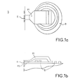
- FIGS. 1a, 1b show the structure of a magnetic head in a thin layer of the traditional type (non-planar).
- This head comprises two stacked magnetic poles P1, P2, magnetically coupled at one end to close the magnetic circuit of the head and comprising a gap E at the other end.
- a magnetic field induction conductor B (winding) is located between the poles P1, P2 to induce a magnetic field in the head.
- the active area of the magnetic head for reading or writing information is located at the end of the air gap E (on the left in Figures 1a, 1b).
- This head is produced by photolithographic deposition and machining of the layers constituting the magnetic poles, the conductors and the insulators. The support is then sawn near the air gap and the head is polished along a plane perpendicular to the photolithography plane. These heads require non-collective polishing steps and are therefore of high cost.
- Figures 2a, 2b show a so-called planar structure head.
- This head has two magnetic poles 4, 5 substantially located in the same plane. The most distant ends of these poles are magnetically coupled to a magnetic sublayer 1 to close the magnetic circuit of the head. The nearest ends are separated by an air gap 6.
- One or more magnetic field induction conductors are located between the magnetic pole (4, 5) and the magnetic sublayer 1.
- This head is produced by deposits, photolithography and collective polishing of the surface. A final sawing allows the heads to be separated. This process is collective in all stages and therefore less expensive; it also allows the creation of matrix arrays of heads as shown in FIG. 3.
- planar heads have a small air gap depth; this is a potential advantage since the inductance of the winding is reduced; this further reduces the noise voltage at the input of the preamplifier of reading.
- the flux must travel a long way in the magnetic poles before bypassing the winding plane; if the permeability of the poles is not very high there is leakage of the flow through this plane and this considerably reduces the efficiency of the head.
- the total permeance of a magnetic circuit is equal to the inductance per square turn of the winding which crosses it.
- the efficiency of a magnetic head is generally called the ratio between the circulation of the field in the air gap and the current injected into the winding expressed in Ampere-turns.
- a head is all the better as its efficiency is close to unity and its permeance is low.
- FIG. 5a shows typical values of permeance of the magnetic circuit of the head of FIG. 2.
- the flux circulating at the birth of the upper poles tends to be short-circuited by the proximity of the lower pole; this results not only in an increase in the impedance of the winding but also due to the limited permeability of the poles a decrease in the efficiency of the head.
- the invention relates to a magnetic head structure which does not have this drawback.
- the plane of the first magnetic layer comprises a second zone of insulating material located under the magnetic poles between the first ends and not comprising magnetic material.
- This head comprises, like that of FIGS. 2a and 2b, a magnetic layer 1 above which are located two magnetic poles in layers 4 and 5 contained substantially in the same plane. These two poles are separated from layer 1 by an insulating layer. These two poles at their ends 40 and 50 are magnetically coupled to the layer 1. The opposite ends 41 and 51 of the poles are separated by an air gap 6. At least one winding conductor 2 is located under one of the magnetic poles to induce a magnetic field. In Figures 4a and 4b, there is shown by way of example two windings each surrounding a pole.
- the operation of the head will be such that it will make it possible to write information on a magnetic information carrier BM such as that shown in broken lines in FIG. 4b. This registration will be done using the magnetic flux passing from the end 41 of the pole 4 to the end 51 of the pole 5.
- a zone 7 not comprising magnetic material there is provided in the plane of the magnetic layer 1, under the magnetic poles and in particular under the air gap 6, a zone 7 not comprising magnetic material.
- This zone preferably includes the zone situated under the conductors 2, the poles 4, 5 and the air gap 6. It is even possible to envisage that the entire zone situated under the poles is non-magnetic, except of course the parts of layer 1 which are magnetically coupled to the ends 40 and 50.
- FIG. 5b represents an example of a magnetic head according to the invention on which the permeance values of the different portions of the magnetic circuit have been indicated. It appears that the magnetic head according to the invention (FIG. 5b) provides characteristics which contribute to producing a magnetic head more efficient than the magnetic heads known in the art such as that of FIG. 5a.
- the invention is applicable to a head with matrix organization comprising several magnetic heads controlled by conductors of magnetic field induction lines and conductors of magnetic field induction columns.
- the poles can be made as described in French patent application No. 2,605,783.
Landscapes
- Engineering & Computer Science (AREA)
- Manufacturing & Machinery (AREA)
- Magnetic Heads (AREA)
Applications Claiming Priority (2)
| Application Number | Priority Date | Filing Date | Title |
|---|---|---|---|
| FR9510658A FR2738657B1 (fr) | 1995-09-12 | 1995-09-12 | Tete magnetique d'enregistrement/lecture |
| FR9510658 | 1995-09-12 |
Publications (3)
| Publication Number | Publication Date |
|---|---|
| EP0762388A2 true EP0762388A2 (de) | 1997-03-12 |
| EP0762388A3 EP0762388A3 (de) | 1997-03-19 |
| EP0762388B1 EP0762388B1 (de) | 2003-11-19 |
Family
ID=9482460
Family Applications (1)
| Application Number | Title | Priority Date | Filing Date |
|---|---|---|---|
| EP96401926A Expired - Lifetime EP0762388B1 (de) | 1995-09-12 | 1996-09-10 | Magnetaufzeichnungs-/-wiedergabekopf |
Country Status (5)
| Country | Link |
|---|---|
| US (1) | US5745329A (de) |
| EP (1) | EP0762388B1 (de) |
| JP (1) | JPH09120506A (de) |
| DE (1) | DE69630745T2 (de) |
| FR (1) | FR2738657B1 (de) |
Families Citing this family (7)
| Publication number | Priority date | Publication date | Assignee | Title |
|---|---|---|---|---|
| FR2723243B1 (fr) * | 1994-07-26 | 1996-09-06 | Thomson Csf | Dispositif d'enregistrement et/ou de lecture de tetes magnetiques et son procede de realisation |
| FR2786345B1 (fr) | 1998-11-24 | 2001-02-09 | Thomson Csf | Dispositif de cryptage quantique |
| US7149173B2 (en) * | 2000-10-17 | 2006-12-12 | Thales | Medium for recording optically readable data, method for making same and optical system reproducing said data |
| FR2824905B1 (fr) * | 2001-05-15 | 2003-08-29 | Thomson Csf | Gyrometre a fibre optique |
| JP4674817B2 (ja) * | 2006-05-09 | 2011-04-20 | セイコーインスツル株式会社 | 近接場光ヘッド及び情報記録再生装置 |
| US8014100B2 (en) * | 2007-05-04 | 2011-09-06 | International Business Machines Corporation | Planar servo write head |
| WO2011002071A1 (ja) * | 2009-06-30 | 2011-01-06 | 国立大学法人北海道大学 | プローブおよびその製造方法ならびにプローブ顕微鏡ならびに磁気ヘッドおよびその製造方法ならびに磁気記録再生装置 |
Family Cites Families (13)
| Publication number | Priority date | Publication date | Assignee | Title |
|---|---|---|---|---|
| JPS5924422A (ja) * | 1982-07-30 | 1984-02-08 | Toshiba Corp | 磁気ヘツド |
| JPS61120313A (ja) * | 1984-11-14 | 1986-06-07 | Sanyo Electric Co Ltd | 薄膜磁気ヘツド |
| JPS62114112A (ja) * | 1985-11-13 | 1987-05-25 | Matsushita Electric Ind Co Ltd | 薄膜磁気ヘツド |
| FR2605783B1 (fr) * | 1986-10-28 | 1992-05-15 | Thomson Csf | T ete magnetique d'enregistrement/lecture en couches minces et son procede de realisation |
| JPH01182908A (ja) * | 1988-01-13 | 1989-07-20 | Hitachi Ltd | 薄膜磁気ヘツド |
| JPH01264619A (ja) * | 1988-04-15 | 1989-10-20 | Seiko Epson Corp | 薄膜磁気ヘッド |
| FR2630244B1 (fr) * | 1988-04-15 | 1990-07-13 | Commissariat Energie Atomique | Dispositif d'ecriture et de lecture sur un support magnetique et son procede de fabrication |
| FR2630853B1 (fr) * | 1988-04-27 | 1995-06-02 | Thomson Csf | Dispositif matriciel a tetes magnetiques notamment en couches minces |
| JPH01275059A (ja) * | 1988-04-27 | 1989-11-02 | Seiko Epson Corp | 磁気ヘッドの製造方法 |
| FR2646000B1 (fr) * | 1989-04-14 | 1995-07-21 | Thomson Csf | Tete magnetique statique de lecture |
| FR2649526B1 (fr) * | 1989-07-04 | 1991-09-20 | Thomson Csf | Procede de fabrication de tetes magnetiques planaires par alveolage d'une plaquette non magnetique, et tetes magnetiques obtenues par un tel procede |
| JPH0440613A (ja) * | 1990-06-07 | 1992-02-12 | Mitsubishi Electric Corp | 薄膜磁気ヘッド素子 |
| JP3200060B2 (ja) * | 1990-09-12 | 2001-08-20 | ソニー株式会社 | 薄膜磁気ヘッド |
-
1995
- 1995-09-12 FR FR9510658A patent/FR2738657B1/fr not_active Expired - Fee Related
-
1996
- 1996-09-10 EP EP96401926A patent/EP0762388B1/de not_active Expired - Lifetime
- 1996-09-10 DE DE69630745T patent/DE69630745T2/de not_active Expired - Fee Related
- 1996-09-11 US US08/712,491 patent/US5745329A/en not_active Expired - Lifetime
- 1996-09-12 JP JP8242149A patent/JPH09120506A/ja active Pending
Also Published As
| Publication number | Publication date |
|---|---|
| FR2738657B1 (fr) | 1997-10-03 |
| EP0762388B1 (de) | 2003-11-19 |
| DE69630745T2 (de) | 2004-09-30 |
| US5745329A (en) | 1998-04-28 |
| DE69630745D1 (de) | 2003-12-24 |
| FR2738657A1 (fr) | 1997-03-14 |
| EP0762388A3 (de) | 1997-03-19 |
| JPH09120506A (ja) | 1997-05-06 |
Similar Documents
| Publication | Publication Date | Title |
|---|---|---|
| EP0420755B1 (de) | Herstellungsverfahren eines Magnetaufzeichnungskopfes und nach diesem Verfahren erhaltener Kopf | |
| EP0340085B1 (de) | Magnetkopf-Matrixanordnung, insbesondere aus Dünnfilmen | |
| EP0652550B1 (de) | Lesemagnetkopf mit Mehrschichtmagnetowiderstandselement und Konzentrator und Herstellungsverfahren | |
| EP0284495B1 (de) | Magnetkopf zum Lesen von Spuren mit sehr schmaler Breite und Herstellungverfahren | |
| EP0618568B1 (de) | Dünnschicht-Aufnahme-Wiedergabemagnetkopf und Herstellungsverfahren | |
| FR2830971A1 (fr) | Dispositif magnetoresistif a vanne de spin a performances ameliorees | |
| EP0188944A1 (de) | System für senkrechte Aufzeichnung und Verfahren zur Herstellung eines Magnetkopfes | |
| EP0406362B1 (de) | Herstellungsverfahren eines aufnahme-/wiedergabekopfes und nach diesem verfahren erhaltener kopf | |
| EP0762388B1 (de) | Magnetaufzeichnungs-/-wiedergabekopf | |
| EP0714090B1 (de) | Aufzeichnungs/-wiedergabemagnetkopf und Herstellungsverfahren | |
| EP0409675B1 (de) | Mehrspur-Magnetkopf mit grossem Feldkontrast | |
| EP0429598B1 (de) | Mehrspur-aufnahmemagnetkopf mit kompakter matrixartiger struktur | |
| EP0463908B1 (de) | Magnetaufzeichnungsvorrichtung mit einer Mehrzahl von Magnetköpfen | |
| EP0314557A2 (de) | Supraleitendes Material aufweisender Aufzeichnungs-/Wiedergabemagnetkopf | |
| EP0644528B1 (de) | Aufzeichnungs- und Wiedergabemagnetkopf mit bezüglich Aufzeichnung kompensiertem Magnetowiderstandselement | |
| EP0215832B1 (de) | Elektromagnet mit grosser magnetfeldhomogenität | |
| FR2712419A1 (fr) | Tête magnétique d'enregistrement/lecture. | |
| FR2622336A1 (fr) | Tete magnetique de lecture et d'enregistrement | |
| EP0716410A2 (de) | Herstellungsverfahren für Aufzeichnungs-/Wiedergabemagnetkopf und Aufzeichnungs-/Wiedergabekopf | |
| FR2606920A1 (fr) | Tete magnetique pour pistes magnetiques a fort champ coercitif et procede de fabrication | |
| JPH10188215A (ja) | 録再分離複合型磁気ヘッド |
Legal Events
| Date | Code | Title | Description |
|---|---|---|---|
| PUAI | Public reference made under article 153(3) epc to a published international application that has entered the european phase |
Free format text: ORIGINAL CODE: 0009012 |
|
| PUAL | Search report despatched |
Free format text: ORIGINAL CODE: 0009013 |
|
| AK | Designated contracting states |
Kind code of ref document: A2 Designated state(s): DE GB IT NL |
|
| AK | Designated contracting states |
Kind code of ref document: A3 Designated state(s): DE GB IT NL |
|
| 17P | Request for examination filed |
Effective date: 19970410 |
|
| RAP1 | Party data changed (applicant data changed or rights of an application transferred) |
Owner name: THALES |
|
| 17Q | First examination report despatched |
Effective date: 20020213 |
|
| GRAH | Despatch of communication of intention to grant a patent |
Free format text: ORIGINAL CODE: EPIDOS IGRA |
|
| GRAH | Despatch of communication of intention to grant a patent |
Free format text: ORIGINAL CODE: EPIDOS IGRA |
|
| GRAA | (expected) grant |
Free format text: ORIGINAL CODE: 0009210 |
|
| AK | Designated contracting states |
Kind code of ref document: B1 Designated state(s): DE GB IT NL |
|
| REG | Reference to a national code |
Ref country code: GB Ref legal event code: FG4D Free format text: NOT ENGLISH |
|
| REF | Corresponds to: |
Ref document number: 69630745 Country of ref document: DE Date of ref document: 20031224 Kind code of ref document: P |
|
| GBT | Gb: translation of ep patent filed (gb section 77(6)(a)/1977) |
Effective date: 20040130 |
|
| PGFP | Annual fee paid to national office [announced via postgrant information from national office to epo] |
Ref country code: NL Payment date: 20040905 Year of fee payment: 9 |
|
| PLBE | No opposition filed within time limit |
Free format text: ORIGINAL CODE: 0009261 |
|
| STAA | Information on the status of an ep patent application or granted ep patent |
Free format text: STATUS: NO OPPOSITION FILED WITHIN TIME LIMIT |
|
| 26N | No opposition filed |
Effective date: 20040820 |
|
| PG25 | Lapsed in a contracting state [announced via postgrant information from national office to epo] |
Ref country code: NL Free format text: LAPSE BECAUSE OF NON-PAYMENT OF DUE FEES Effective date: 20060401 |
|
| NLV4 | Nl: lapsed or anulled due to non-payment of the annual fee |
Effective date: 20060401 |
|
| PGFP | Annual fee paid to national office [announced via postgrant information from national office to epo] |
Ref country code: IT Payment date: 20080926 Year of fee payment: 13 |
|
| PGFP | Annual fee paid to national office [announced via postgrant information from national office to epo] |
Ref country code: GB Payment date: 20080910 Year of fee payment: 13 |
|
| PGFP | Annual fee paid to national office [announced via postgrant information from national office to epo] |
Ref country code: DE Payment date: 20080926 Year of fee payment: 13 |
|
| GBPC | Gb: european patent ceased through non-payment of renewal fee |
Effective date: 20090910 |
|
| PG25 | Lapsed in a contracting state [announced via postgrant information from national office to epo] |
Ref country code: DE Free format text: LAPSE BECAUSE OF NON-PAYMENT OF DUE FEES Effective date: 20100401 |
|
| PG25 | Lapsed in a contracting state [announced via postgrant information from national office to epo] |
Ref country code: GB Free format text: LAPSE BECAUSE OF NON-PAYMENT OF DUE FEES Effective date: 20090910 |
|
| PG25 | Lapsed in a contracting state [announced via postgrant information from national office to epo] |
Ref country code: IT Free format text: LAPSE BECAUSE OF NON-PAYMENT OF DUE FEES Effective date: 20090910 |