EP0762485A2 - Verfahren zur Kontaktlochherstellung - Google Patents
Verfahren zur Kontaktlochherstellung Download PDFInfo
- Publication number
- EP0762485A2 EP0762485A2 EP96113851A EP96113851A EP0762485A2 EP 0762485 A2 EP0762485 A2 EP 0762485A2 EP 96113851 A EP96113851 A EP 96113851A EP 96113851 A EP96113851 A EP 96113851A EP 0762485 A2 EP0762485 A2 EP 0762485A2
- Authority
- EP
- European Patent Office
- Prior art keywords
- mask
- contact hole
- areas
- active
- regions
- Prior art date
- Legal status (The legal status is an assumption and is not a legal conclusion. Google has not performed a legal analysis and makes no representation as to the accuracy of the status listed.)
- Granted
Links
Images
Classifications
-
- H—ELECTRICITY
- H10—SEMICONDUCTOR DEVICES; ELECTRIC SOLID-STATE DEVICES NOT OTHERWISE PROVIDED FOR
- H10W—GENERIC PACKAGES, INTERCONNECTIONS, CONNECTORS OR OTHER CONSTRUCTIONAL DETAILS OF DEVICES COVERED BY CLASS H10
- H10W20/00—Interconnections in chips, wafers or substrates
- H10W20/01—Manufacture or treatment
- H10W20/071—Manufacture or treatment of dielectric parts thereof
- H10W20/081—Manufacture or treatment of dielectric parts thereof by forming openings in the dielectric parts
-
- H—ELECTRICITY
- H10—SEMICONDUCTOR DEVICES; ELECTRIC SOLID-STATE DEVICES NOT OTHERWISE PROVIDED FOR
- H10D—INORGANIC ELECTRIC SEMICONDUCTOR DEVICES
- H10D30/00—Field-effect transistors [FET]
- H10D30/01—Manufacture or treatment
- H10D30/021—Manufacture or treatment of FETs having insulated gates [IGFET]
- H10D30/031—Manufacture or treatment of FETs having insulated gates [IGFET] of thin-film transistors [TFT]
- H10D30/0321—Manufacture or treatment of FETs having insulated gates [IGFET] of thin-film transistors [TFT] comprising silicon, e.g. amorphous silicon or polysilicon
- H10D30/0323—Manufacture or treatment of FETs having insulated gates [IGFET] of thin-film transistors [TFT] comprising silicon, e.g. amorphous silicon or polysilicon comprising monocrystalline silicon
-
- H—ELECTRICITY
- H10—SEMICONDUCTOR DEVICES; ELECTRIC SOLID-STATE DEVICES NOT OTHERWISE PROVIDED FOR
- H10W—GENERIC PACKAGES, INTERCONNECTIONS, CONNECTORS OR OTHER CONSTRUCTIONAL DETAILS OF DEVICES COVERED BY CLASS H10
- H10W10/00—Isolation regions in semiconductor bodies between components of integrated devices
- H10W10/01—Manufacture or treatment
- H10W10/011—Manufacture or treatment of isolation regions comprising dielectric materials
- H10W10/012—Manufacture or treatment of isolation regions comprising dielectric materials using local oxidation of silicon [LOCOS]
Definitions
- the invention relates to a method for producing contact holes in MOS circuits using SOI technology with an oxide layer and an overlying silicon layer.
- circuits are formed in a thin silicon film that is arranged on an insulator.
- the properties of these circuits are particularly favorable when the active silicon layer is so thin that a so-called “fully depleted", that is to say a zone free of charge carriers, arises in the active silicon region.
- the thickness required for this is preferably in the order of 50 to 80 nm.
- the invention has for its object to provide a method of the type mentioned, in which the production of the contact holes and the entire process control is particularly safe while providing an extremely thin active area.
- the silicon layer lying on the oxide layer which is also referred to as a body, is formed with a thickness that is greater than the thickness required for the active regions of the MOS circuits, a first mask is applied to the contact hole regions and the uncovered areas are thinned to a thickness suitable for the active areas and the active areas, the lead areas and contact hole areas are covered with a second mask, and the uncovered areas are oxidized with a LOCOS insulation and in further steps a connection to the active area and a Insulating layer generated, the actual contact hole etching takes place through the insulating layer.
- This method makes extremely thin silicon areas for "fully depleted" MOS circuits and areas with local thicker silicon for sufficient process reliability in the production of contact holes and at the same time applied a process control compatible with the LOCOS insulation, with which particularly precise oxidation can be carried out.
- the contact hole regions and therefore also the original silicon layer are formed thickened, since an etching into the contact hole regions is inevitable during the final contact hole etching and the silicon layer in this region must not be completely removed.
- the lead regions in particular the source lead region, are also covered with the first mask. This can reduce the lead resistance from the contact area to the active area. This measure is of particular relevance for the source supply line, but can also be used advantageously for the drain supply line.
- the thinning of the areas not covered by the first mask is also advantageously carried out using a LOCOS technique, since this enables reliable process control.
- the second mask is made larger than the first, so that a certain amount of lead is also created around the contact hole areas.
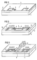
- FIG. 1 shows the SOI base material, which essentially consists of a substrate 1, a buried oxide layer 2 and a silicon layer 3, which is also referred to as a body.
- the thickness of the silicon layer 1 is approximately 170 nm.
- the silicon layer is thus so thick that, after the process-related thinning, the points exposed during the contact hole etching have a thickness which is sufficient for overetch and contact hole aftertreatment.
- a first local oxidation mask which can consist of nitride or oxynitride
- the contact hole regions 4, 5 for the source and the drain connection and also the lead region 6, which in the exemplary embodiment are only embodied in the source lead, are now covered.
- the areas not covered are oxidized to such an extent that the remaining thickness of the silicon layer 1 is so thin that it meets the requirements for "fully depleted", that is to say for completely depleted and thus charge carrier-free MOS devices.
- the silicon layer lying outside the covered areas is first oxidized and then the oxide is removed, so that the thin silicon layer shown in FIG. 1 is formed outside the covered areas. This process step is achieved by local oxidation of the silicon, i.e. by a kind of LOCOS technology.
- a second mask is applied, with which the contact hole regions 4, 5, the active region 8 and the lead regions 6 and 7 are covered.
- This mask is enlarged compared to the first mask so that there is a lead 14 forms around the raised contact hole areas 4, 5, through which the process reliability is further increased.
- an oxidation is carried out with the LOCOS technology.
- the LOCOS technique is carried out completely in an area which was thinned in the first process step and the oxidation must therefore be matched to the thickness of the previously thinned silicon layer. Since there are no different thicknesses in the processed area, significant lateral underoxidation is excluded.
- the LOCOS oxidation creates an increased LOCOS insulation layer 9 outside the contact hole regions 4, 5 of the lead regions 6, 7 of the active region 8 and the leads 14.
Landscapes
- Thin Film Transistor (AREA)
- Internal Circuitry In Semiconductor Integrated Circuit Devices (AREA)
- Electrodes Of Semiconductors (AREA)
- Local Oxidation Of Silicon (AREA)
- Metal-Oxide And Bipolar Metal-Oxide Semiconductor Integrated Circuits (AREA)
Abstract
Description
- Die Erfindung betrifft ein Verfahren zur Kontaktlochherstellung bei MOS-Schaltkreisen in SOI-Technik mit einer Oxidschicht und einer darüberliegenden Siliziumschicht.
- In der SOI-Technik werden Schaltkreise in einem dünnen Siliziumfilm ausgebildet, der auf einem Isolator angeordnet ist. Die Eigenschaften dieser Schaltkreise sind insbesondere dann günstig, wenn die aktive Siliziumschicht so dünn ist, daß eine sogenannte "fully depleted", also eine ladungsträgerfreie Zone im aktiven Siliziumbereich entsteht. Bei sogenannten "surface channel-Schaltungen" und Anwendung der Sub-µm-Technologie liegt die dazu benötigte Dicke vorzugsweise in der Größenordnung von 50 bis 80 nm. Diese extrem dünnen Siliziumschichten stellen besondere Anforderungen an die Prozeßführung, insbesondere an die isotropen Ätzungen von Oxidschichten, da diese nicht beliebig selektiv zu Silizium sind. Kann man sich bei den Spacerätzungen durch geänderte Prozeßfolgen helfen, so ist bei der Kontaktlochätzung eine Einätzung unvermeidlich. Außerdem muß nach der Kontaktlochätzung neben den Polymeren auch noch die oberste Siliziumschicht entfernt werden. Diese ist stark gestört und würde einen erhöhten Kontaktwiderstand verursachen.
- Es ist bekannt, die kritischen Kontaktlochätzung durch Wahl eines SOI-Grundmaterials zu umgehen, dessen Siliziumschicht etwas dicker ist, als es für MOS-Schaltungen mit einem vollständig ladungsträgerfreien aktiven Bereich erforderlich wäre. In einem ersten Prozeßblock wird dabei das Silizium im aktiven Bereich auf die gewünschte Dicke gedünnt. Da aber auf dem SOI-Grundmaterial unterschiedliche Dicken vorliegen, ist jetzt eine weitere Prozeßführung mit einer Isolationstechnik durch lokale vollständige Oxidation der Siliziumschicht nur schwer möglich, da bei dieser Technik die Prozeßführung auf die maximale Siliziumschicht abgestellt werden muß. In diesem Fall liegen jedoch auch Bereiche mit einer deutlich kleineren Dicke vor, in denen sich die Oxidation in lateraler Richtung unter die dabei verwendete Nitridmaske fortsetzt, wodurch ein unvertretbar großer Maßverlust gerade in den kritischen aktiven Bereichen entsteht. Anstelle der lokalen vollständigen Oxidation kann auch eine MESA-Ätzung angewandt werden. Dabei treten aber unerwünschte parasitäre Seitenwandtransistoren und Gateoxiddünnungen an der MESA-Kante auf, deren Kontrolle wieder weitere Prozeßmaßnahmen erfordert.
- Der Erfindung liegt die Aufgabe zugrunde, ein Verfahren der eingangs genannten Art zu schaffen, bei dem die Herstellung der Kontaktlöcher sowie die gesamte Prozeßführung bei gleichzeitiger Vorsehung eines extrem dünnen aktiven Bereichs besonders sicher ist.
- Die Lösung dieser Aufgabe erfolgt mit den Merkmalen des Anspruchs 1. Vorteilhafte Weiterbildungen sind in den Unteransprüchen beschrieben.
- Nach dem Grundgedanken der Erfindung wird die auf der Oxidschicht liegende Siliziumschicht, die auch als Body bezeichnet wird, mit einer Dicke ausgebildet, die größer ist als die für die aktiven Bereiche der MOS-Schaltkreise erforderliche Dicke, eine erste Maske auf die Kontaktlochbereiche aufgebracht und die nicht abgedeckten Bereiche auf eine für die aktiven Bereiche geeignete Dicke gedünnt und mit einer zweiten Maske die aktiven Bereiche, die Zuleitungsbereiche und Kontaktlochbereiche abgedeckt, und die nicht abgedeckten Bereiche mit einer LOCOS-Isolation oxidiert und in weiteren Schritten ein Anschluß an den aktiven Bereich und eine Isolierschicht erzeugt, wobei die eigentliche Kontaktlochätzung durch die Isolierschicht hindurch erfolgt.
- Durch dieses Verfahren werden extrem dünne Siliziumbereiche für "fully depleted" MOS-Schaltungen und Bereiche mit lokal dickerem Silizium für eine ausreichende Prozeßsicherheit bei der Herstellung von Kontaktlöchern geschaffen und gleichzeitig eine mit der LOCOS-Isolation verträgliche Prozeßführung angewandt, mit der eine besonders exakte Oxidierung durchführbar ist. Die Kontaktlochbereiche und deshalb auch die ursprüngliche Siliziumschicht werden verdickt ausgebildet, da bei der letztendlichen Kontaktlochätzung eine Einätzung in die Kontaktlochbereiche unvermeidlich ist und die Siliziumschicht in diesem Bereich nicht vollständig entfernt werden darf.
- In einer bevorzugten Weiterbildung der Erfindung werden mit der ersten Maske auch die Zuleitungsbereiche, insbesondere der Source-Zuleitungsbereich, abgedeckt. Dadurch kann der Zuleitungswiderstand vom Kontaktbereich bis an den aktiven Bereich reduziert werden. Diese Maßnahme ist bei der Source-Zuleitung von besonderer Relevanz, kann aber auch bei der Drain-Zuleitung vorteilhaft eingesetzt werden.
- Die Dünnung der nicht von der ersten Maske abgedeckten Bereiche wird günstigerweise ebenfalls mit einer LOCOS-Technik durchgeführt, da diese eine sichere Prozeßführung ermöglicht. Um sicherzustellen, daß die LOCOS-Isolation bei Verwendung der zweiten Maske nur in Bereichen stattfindet, die im ersten Dünnungsschritt bereits gedünnt worden sind, wird die zweite Maske größer als die erste ausgebildet, so daß auch um die Kontaktlochbereiche herum ein gewisser Vorhalt entsteht.
- Die Anwendung dieser Technik bietet bei CMOS-Schaltkreisen und NMOS-Transistoren besondere Vorteile.
- Nachfolgend wird die Erfindung anhand eines in der Zeichnung dargestellten Ausführungsbeispiels weiter erläutert. Die schematischen Darstellungen zeigen beispielhaft verschiedene Stadien des Herstellungsprozesses für CMOS-Transistoren mit lokal dickerem Silizium im Bereich der Kontaktlöcher und den Bereichen der Transistorzuleitungen. Dabei zeigt
- Figur 1
- den Verfahrensstand nach Anwendung einer ersten Maskentechnik;
- Figur 2
- den Verfahrensstand nach Anwendung einer zweiten Maskentechnik; und
- Figur 3
- den Zustand im einem Endstadium des Verfahrens.
- In Figur 1 ist das SOI-Grundmaterial dargestellt, welches im wesentlichen aus einem Substrat 1, einer vergrabenen Oxidschicht 2 und einer Siliziumschicht 3, die auch als Body bezeichnet wird, besteht. Die Dicke der Siliziumschicht 1 beträgt in etwa 170 nm. Damit ist die Siliziumschicht so dick, daß nach den prozeßbedingten Dünnungen die bei der Kontaktlochätzung freiliegenden Stellen eine für Overetch und Kontaktlochnachbehandlung ausreichende Dicke aufweisen. Bei einer ersten lokalen Oxidationsmaske, die aus Nitrid oder Oxynitrid bestehen kann, werden nun die Kontaktlochbereiche 4, 5 für den Source- und den Drainanschluß und auch der Zuleitungsbereich 6, im Ausführungsbeispiel nur in der Source-Zuleitung ausgeführt, abgedeckt. Die nicht abgedeckten Bereiche werden soweit oxidiert, daß die Restdicke der Siliziumschicht 1 so dünn ist, daß sie den Anforderungen für "fully depleted", also für vollständig verarmte und somit ladungsträgerfreie MOS-Einrichtungen entspricht. Dabei wird die außerhalb der abgedeckten Bereiche liegende Siliziumschicht zunächst oxidiert und dann das Oxid abgetragen, so daß die in Figur 1 dargestellte dünne Siliziumschicht außerhalb der abgedeckten Bereiche entsteht. Dieser Verfahrensschritt wird durch lokale Oxidation des Siliziums, also durch eine Art LOCOS-Technik erreicht.
- Im folgenden wird eine zweite Maske aufgebracht, mit der die Kontaktlochbereiche 4, 5, der aktive Bereich 8 sowie die Zuleitungsbereiche 6 und 7 abgedeckt werden. Diese Maske ist gegenüber der ersten Maske vergrößert, so daß sich ein Vorhalt 14 rings um die erhöhten Kontaktlochbereiche 4, 5 ausbildet, durch den die Prozeßsicherheit weiter erhöht wird. Außerhalb der wiederum aus Nitrid oder Oxynitrid bestehenden Oxidationsmaske wird mit der LOCOS-Technik eine Oxidation durchgeführt. Dabei ist herauszustellen, daß die LOCOS-Technik vollständig auf einem Bereich durchgeführt wird, der im ersten Verfahrensschritt gedünnt worden ist und die Oxidation somit auf die Dicke der zuvor gedünnten Siliziumschicht abgestimmt werden muß. Da in dem prozessierten Bereich keine unterschiedlichen Dicken vorkommen, ist eine deutliche laterale Unteroxidation ausgeschlossen. Durch die LOCOS-Oxidation entsteht außerhalb der Kontaktlochbereiche 4, 5 der Zuleitungsbereiche 6, 7 des aktiven Bereichs 8 und der Vorhalte 14 eine erhöhte LOCOS-Isolationsschicht 9.
- In Figur 3 ist der Verfahrensstand nach einigen weiteren Schritten dargestellt. So wird ein Gateanschluß 12 erzeugt, dessen Siliziumzuführung auf den aktiven Bereich 8 geführt ist, der durch die vorausgehenden Prozeßschritte so dünn ist, daß das Silizium möglichst vollständig verarmt ist. Auf die dargestellte Struktur wird noch eine in Figur 3 nicht dargestellte Isolationsschicht aufgebracht, durch die die Kontaktlochätzungen erfolgen. In der Figur sind das Source-Kontaktloch 10, das Drain-Kontaktloch 11 und das Gate-Kontaktloch 13 dargestellt. Bei der Kontaktlochätzung wird ein Teil der Kontaktlochbereiche 4, 5 abgetragen, wobei jedoch die Siliziumschicht in diesem Bereich nicht vollständig entfernt wird, da durch das beschriebene Verfahren diese Bereiche lokal dicker sind und dadurch die Prozeßsicherheit erhöht wird. Der Zuleitungsbereich 6 vom Source-Kontaktlochbereich 4 zum aktiven Bereich 8 ist ebenfalls verdickt ausgebildet, um den Zuleitungswiderstand zu reduzieren. In gleicher Weise könnte auch der Zuleitungsbereich 7 vom Drain-Kontaktlochbereich 5 zum aktiven Bereich 8 ausgebildet werden.
Claims (5)
- Verfahren zur Kontaktlochherstellung bei MOS-Schaltkreisen in SOI-Technik mit einer Oxidschicht (2) und einer darüber liegenden Siliziumschicht (3), bei demdie Siliziumschicht (3) mit einer Dicke ausgebildet wird, die größer ist als die für die aktiven Bereiche der MOS-Schaltkreise erforderliche Dicke,eine erste Maske auf die Kontaktlochbereiche (4, 5) aufgebracht und die nicht abgedeckten Bereiche auf eine für die aktiven Bereiche geeignete Dicke gedünnt werden,mit einer zweiten Maske die aktiven Bereiche (8), die Zuleitungsbereiche (6, 7) und die Kontaktlochbereiche (4, 5) abgedeckt und die nicht abgedeckten Bereiche mit einer LOCOS-Isolation isoliert werden, undin weiteren Schritten ein Anschluß an den aktiven Bereich und eine Isolierschicht erzeugt werden, durch die die Kontaktloch-Ätzung erfolgt.
- Verfahren nach Anspruch 1,
dadurch gekennzeichnet,
daß mit der ersten Maske auch die Zuleitungsbereiche (6, 7), insbesondere der Source-Zuleitungsbereich (6), abgedeckt werden. - Verfahren nach einem der vorhergehenden Ansprüche,
dadurch gekennzeichnet,
daß im Anschluß an die Aufbringung der ersten Maske eine LOCOS-Technik angewandt wird. - Verfahren nach einem der vorhergehenden Ansprüche,
dadurch gekennzeichnet,
daß die zweite Maske größer ist als die erste Maske und Vorhalte (14) um die Kontaktlochbereiche (4, 5) gebildet werden. - Verfahren nach einem der vorhergehenden Ansprüche,
dadurch gekennzeichnet,
daß CMOS-Schaltungen und insbesondere NMOS-Transistoren hergestellt werden.
Applications Claiming Priority (2)
| Application Number | Priority Date | Filing Date | Title |
|---|---|---|---|
| DE19532380A DE19532380A1 (de) | 1995-09-01 | 1995-09-01 | Verfahren zur Kontaktlochherstellung |
| DE19532380 | 1995-09-01 |
Publications (3)
| Publication Number | Publication Date |
|---|---|
| EP0762485A2 true EP0762485A2 (de) | 1997-03-12 |
| EP0762485A3 EP0762485A3 (de) | 1999-05-06 |
| EP0762485B1 EP0762485B1 (de) | 2002-12-11 |
Family
ID=7771077
Family Applications (1)
| Application Number | Title | Priority Date | Filing Date |
|---|---|---|---|
| EP96113851A Expired - Lifetime EP0762485B1 (de) | 1995-09-01 | 1996-08-29 | Verfahren zur Kontaktlochherstellung |
Country Status (6)
| Country | Link |
|---|---|
| US (1) | US5728609A (de) |
| EP (1) | EP0762485B1 (de) |
| JP (1) | JPH09106960A (de) |
| KR (1) | KR970018089A (de) |
| DE (2) | DE19532380A1 (de) |
| TW (1) | TW332315B (de) |
Families Citing this family (1)
| Publication number | Priority date | Publication date | Assignee | Title |
|---|---|---|---|---|
| JP3265569B2 (ja) * | 1998-04-15 | 2002-03-11 | 日本電気株式会社 | 半導体装置及びその製造方法 |
Family Cites Families (2)
| Publication number | Priority date | Publication date | Assignee | Title |
|---|---|---|---|---|
| US4753896A (en) * | 1986-11-21 | 1988-06-28 | Texas Instruments Incorporated | Sidewall channel stop process |
| US5572040A (en) * | 1993-07-12 | 1996-11-05 | Peregrine Semiconductor Corporation | High-frequency wireless communication system on a single ultrathin silicon on sapphire chip |
-
1995
- 1995-09-01 DE DE19532380A patent/DE19532380A1/de not_active Withdrawn
-
1996
- 1996-08-22 TW TW085110242A patent/TW332315B/zh active
- 1996-08-29 DE DE59609964T patent/DE59609964D1/de not_active Expired - Fee Related
- 1996-08-29 EP EP96113851A patent/EP0762485B1/de not_active Expired - Lifetime
- 1996-08-30 KR KR1019960036624A patent/KR970018089A/ko not_active Abandoned
- 1996-08-30 JP JP8249273A patent/JPH09106960A/ja active Pending
- 1996-09-03 US US08/706,820 patent/US5728609A/en not_active Expired - Fee Related
Non-Patent Citations (3)
| Title |
|---|
| CHOI JH ET AL: "EXTREMELY THIN FILM (10NM) SOI MOSFET CHARACTERISTICS INCLUDING INVERSION LAYER TO ACCUMULATION LAYER TUNNELING" INTERNATIONAL ELECTRON DEVICES MEETING 1994,Dezember 1994, Seiten 645-648, XP000585572 INSTITUTE OF ELECTRICAL AND ELECTRONICS ENGINEERS * |
| FAYNOT O ET AL: "HIGH PERFORMANCE ULTRATHIN SOI MOSFET'S OBTAINED BY LOCALIZED OXIDATION" IEEE ELECTRON DEVICE LETTERS, Bd. 15, Nr. 5, 1. Mai 1994, Seiten 175-177, XP000449442 * |
| RAYNAUD C ET AL: "HIGH PERFORMANCE SUBMICRON SOI DEVICES WITH SILICON FILM THICKNESS BELOW 50NM" INTERNATIONAL SOI CONFERENCE PROCEEDINGS, NANTUCKET ISLAND, OCT. 3 - 6, 1994, 3. Oktober 1994, Seite 55/56 XP000512317 INSTITUTE OF ELECTRICAL AND ELECTRONICS ENGINEERS * |
Also Published As
| Publication number | Publication date |
|---|---|
| TW332315B (en) | 1998-05-21 |
| DE59609964D1 (de) | 2003-01-23 |
| JPH09106960A (ja) | 1997-04-22 |
| US5728609A (en) | 1998-03-17 |
| KR970018089A (ko) | 1997-04-30 |
| DE19532380A1 (de) | 1997-03-06 |
| EP0762485B1 (de) | 2002-12-11 |
| EP0762485A3 (de) | 1999-05-06 |
Similar Documents
| Publication | Publication Date | Title |
|---|---|---|
| DE2832388C2 (de) | Verfahren zum Herstellen von MNOS- und MOS-Transistoren in Silizium-Gate-Technologie auf einem Halbleitersubstrat | |
| DE4235534C2 (de) | Verfahren zum Isolieren von Feldeffekttransistoren | |
| DE3485880T2 (de) | Verfahren zur herstellung von halbleiteranordnungen. | |
| DE69615458T2 (de) | Dünnfilmtransistor über einem isolierten Halbleitersubstrat und Verfahren zur Herstellung | |
| DE3011982C2 (de) | ||
| DE19605235A1 (de) | Halbleitereinrichtung und Verfahren zur Herstellung einer Halbleitereinrichtung | |
| DE2923995A1 (de) | Verfahren zum herstellen von integrierten mos-schaltungen mit und ohne mnos-speichertransistoren in silizium-gate-technologie | |
| DE69627975T2 (de) | MOS-Transistor und Verfahren zu seiner Herstellung | |
| DE19623846A1 (de) | Halbleitereinrichtung | |
| DE4413815A1 (de) | Herstellungsverfahren für eine Halbleitervorrichtung | |
| DE10012141A1 (de) | Verfahren zur Herstellung eines Einzelelektron-Transistors | |
| DE2546314A1 (de) | Feldeffekt-transistorstruktur und verfahren zur herstellung | |
| DE2531927A1 (de) | Polykristallines silizium-widerstandselement fuer integrierte schaltungen | |
| DE4221039C2 (de) | Verfahren zur Herstellung einer Halbleitervorrichtung mit einem vertikalen Halbleiterelement und einem weiteren Halbleiterbauelement | |
| DE4139039C2 (de) | MOS-Halbleitervorrichtung | |
| DE2420239A1 (de) | Verfahren zur herstellung doppelt diffundierter lateraler transistoren | |
| DE69231484T2 (de) | Verfahren zur Herstellung von Isolationszonen des LOCOS-Typs für integrierte Schaltungen vom MOS-Typ | |
| DE2047672A1 (de) | Hochfrequenz Feldeffekttransistor | |
| DE69614326T2 (de) | Mosfet mit niedrigem leckstrom | |
| DE2918888C2 (de) | MNOS-Speicherzelle und Verfahren zu ihrem Betrieb sowie zu ihrer Herstellung | |
| DE19900610A1 (de) | Leistungshalbleiterbauelement mit halbisolierendem polykristallinem Silicium und Herstellungsverfahren hierfür | |
| DE3932445C2 (de) | Komplementäre Halbleitereinrichtung mit einem verbesserten Isolationsbereich | |
| DE19830543B4 (de) | Halbleitereinrichtung mit Hohlraum zwischen den Isolationsseitenwandstücken und dem Halbleitersubstrat und Verfahren zu ihrer Herstellung | |
| EP0762485B1 (de) | Verfahren zur Kontaktlochherstellung | |
| DE102007007096B4 (de) | Halbleitervorrichtung und Verfahren zur Herstellung derselben |
Legal Events
| Date | Code | Title | Description |
|---|---|---|---|
| PUAI | Public reference made under article 153(3) epc to a published international application that has entered the european phase |
Free format text: ORIGINAL CODE: 0009012 |
|
| AK | Designated contracting states |
Kind code of ref document: A2 Designated state(s): DE FR GB IT |
|
| PUAL | Search report despatched |
Free format text: ORIGINAL CODE: 0009013 |
|
| AK | Designated contracting states |
Kind code of ref document: A3 Designated state(s): DE FR GB IT |
|
| 17P | Request for examination filed |
Effective date: 19990607 |
|
| RAP1 | Party data changed (applicant data changed or rights of an application transferred) |
Owner name: INFINEON TECHNOLOGIES AG |
|
| 17Q | First examination report despatched |
Effective date: 20010914 |
|
| GRAG | Despatch of communication of intention to grant |
Free format text: ORIGINAL CODE: EPIDOS AGRA |
|
| GRAG | Despatch of communication of intention to grant |
Free format text: ORIGINAL CODE: EPIDOS AGRA |
|
| GRAH | Despatch of communication of intention to grant a patent |
Free format text: ORIGINAL CODE: EPIDOS IGRA |
|
| GRAH | Despatch of communication of intention to grant a patent |
Free format text: ORIGINAL CODE: EPIDOS IGRA |
|
| GRAA | (expected) grant |
Free format text: ORIGINAL CODE: 0009210 |
|
| AK | Designated contracting states |
Kind code of ref document: B1 Designated state(s): DE FR GB IT |
|
| REG | Reference to a national code |
Ref country code: GB Ref legal event code: FG4D Free format text: NOT ENGLISH |
|
| REF | Corresponds to: |
Ref document number: 59609964 Country of ref document: DE Date of ref document: 20030123 |
|
| GBT | Gb: translation of ep patent filed (gb section 77(6)(a)/1977) |
Effective date: 20030315 |
|
| ET | Fr: translation filed | ||
| PLBE | No opposition filed within time limit |
Free format text: ORIGINAL CODE: 0009261 |
|
| STAA | Information on the status of an ep patent application or granted ep patent |
Free format text: STATUS: NO OPPOSITION FILED WITHIN TIME LIMIT |
|
| 26N | No opposition filed |
Effective date: 20030912 |
|
| PGFP | Annual fee paid to national office [announced via postgrant information from national office to epo] |
Ref country code: FR Payment date: 20060817 Year of fee payment: 11 |
|
| PGFP | Annual fee paid to national office [announced via postgrant information from national office to epo] |
Ref country code: GB Payment date: 20060824 Year of fee payment: 11 |
|
| PGFP | Annual fee paid to national office [announced via postgrant information from national office to epo] |
Ref country code: IT Payment date: 20060831 Year of fee payment: 11 |
|
| PGFP | Annual fee paid to national office [announced via postgrant information from national office to epo] |
Ref country code: DE Payment date: 20061017 Year of fee payment: 11 |
|
| GBPC | Gb: european patent ceased through non-payment of renewal fee |
Effective date: 20070829 |
|
| REG | Reference to a national code |
Ref country code: FR Ref legal event code: ST Effective date: 20080430 |
|
| PG25 | Lapsed in a contracting state [announced via postgrant information from national office to epo] |
Ref country code: DE Free format text: LAPSE BECAUSE OF NON-PAYMENT OF DUE FEES Effective date: 20080301 |
|
| PG25 | Lapsed in a contracting state [announced via postgrant information from national office to epo] |
Ref country code: FR Free format text: LAPSE BECAUSE OF NON-PAYMENT OF DUE FEES Effective date: 20070831 |
|
| PG25 | Lapsed in a contracting state [announced via postgrant information from national office to epo] |
Ref country code: GB Free format text: LAPSE BECAUSE OF NON-PAYMENT OF DUE FEES Effective date: 20070829 |
|
| PG25 | Lapsed in a contracting state [announced via postgrant information from national office to epo] |
Ref country code: IT Free format text: LAPSE BECAUSE OF NON-PAYMENT OF DUE FEES Effective date: 20070829 |