EP0762549A2 - Connecteur électrique - Google Patents
Connecteur électrique Download PDFInfo
- Publication number
- EP0762549A2 EP0762549A2 EP96113146A EP96113146A EP0762549A2 EP 0762549 A2 EP0762549 A2 EP 0762549A2 EP 96113146 A EP96113146 A EP 96113146A EP 96113146 A EP96113146 A EP 96113146A EP 0762549 A2 EP0762549 A2 EP 0762549A2
- Authority
- EP
- European Patent Office
- Prior art keywords
- housing part
- contact elements
- lower housing
- electrical connector
- connection points
- Prior art date
- Legal status (The legal status is an assumption and is not a legal conclusion. Google has not performed a legal analysis and makes no representation as to the accuracy of the status listed.)
- Granted
Links
Images


Classifications
-
- H—ELECTRICITY
- H01—ELECTRIC ELEMENTS
- H01R—ELECTRICALLY-CONDUCTIVE CONNECTIONS; STRUCTURAL ASSOCIATIONS OF A PLURALITY OF MUTUALLY-INSULATED ELECTRICAL CONNECTING ELEMENTS; COUPLING DEVICES; CURRENT COLLECTORS
- H01R43/00—Apparatus or processes specially adapted for manufacturing, assembling, maintaining, or repairing of line connectors or current collectors or for joining electric conductors
- H01R43/20—Apparatus or processes specially adapted for manufacturing, assembling, maintaining, or repairing of line connectors or current collectors or for joining electric conductors for assembling or disassembling contact members with insulating base, case or sleeve
-
- H—ELECTRICITY
- H01—ELECTRIC ELEMENTS
- H01R—ELECTRICALLY-CONDUCTIVE CONNECTIONS; STRUCTURAL ASSOCIATIONS OF A PLURALITY OF MUTUALLY-INSULATED ELECTRICAL CONNECTING ELEMENTS; COUPLING DEVICES; CURRENT COLLECTORS
- H01R43/00—Apparatus or processes specially adapted for manufacturing, assembling, maintaining, or repairing of line connectors or current collectors or for joining electric conductors
- H01R43/16—Apparatus or processes specially adapted for manufacturing, assembling, maintaining, or repairing of line connectors or current collectors or for joining electric conductors for manufacturing contact members, e.g. by punching and by bending
-
- H—ELECTRICITY
- H01—ELECTRIC ELEMENTS
- H01R—ELECTRICALLY-CONDUCTIVE CONNECTIONS; STRUCTURAL ASSOCIATIONS OF A PLURALITY OF MUTUALLY-INSULATED ELECTRICAL CONNECTING ELEMENTS; COUPLING DEVICES; CURRENT COLLECTORS
- H01R13/00—Details of coupling devices of the kinds covered by groups H01R12/70 or H01R24/00 - H01R33/00
- H01R13/46—Bases; Cases
- H01R13/502—Bases; Cases composed of different pieces
- H01R13/506—Bases; Cases composed of different pieces assembled by snap action of the parts
-
- H—ELECTRICITY
- H01—ELECTRIC ELEMENTS
- H01R—ELECTRICALLY-CONDUCTIVE CONNECTIONS; STRUCTURAL ASSOCIATIONS OF A PLURALITY OF MUTUALLY-INSULATED ELECTRICAL CONNECTING ELEMENTS; COUPLING DEVICES; CURRENT COLLECTORS
- H01R13/00—Details of coupling devices of the kinds covered by groups H01R12/70 or H01R24/00 - H01R33/00
- H01R13/66—Structural association with built-in electrical component
- H01R13/6608—Structural association with built-in electrical component with built-in single component
- H01R13/6633—Structural association with built-in electrical component with built-in single component with inductive component, e.g. transformer
Definitions
- the invention relates to a connector according to the preamble of claim 1.
- a connector for an airbag system in the housing of which, in addition to an electrical component, a plurality of stamped contact elements are arranged, which are equipped with plug contacts for connecting corresponding connecting lines.
- Such connectors are dimensioned extremely small due to the limited space in motor vehicles, so that the positioning and connection of individual contact elements in the housing is extremely precise and accordingly expensive.
- DE 43 10 369 C2 describes a contact set for a connector which is made from a one-piece stamped and bent part. After the shaping process has been completed, the non-separated stamped and bent part is assembled with an electrical component and with connecting lines. Only then is the stamped and bent part separated into individual conductor tracks, either immediately afterwards or by closing a two-part housing, with cutting pins on the housing separating the inserted contact set at predetermined breaking points.
- the special design of the housing is shown in DE 44 13 756 C1, at least one housing part having means for positioning and locking the contact set, which do not require any additional method steps.
- the complexity of the assembled contact set before installation in the housing, regardless of whether the conductor tracks have already been separated, requires extremely complex and correspondingly expensive handling technology due to the minimal dimensions of the connector.
- a dimensionally stable plastic part consisting of two half-shells is provided to cover the transition from a cable harness to a plug.
- the two Half-shells are hinged together and foldable lockable.
- EP 0 332 866 A2 describes a manufacturing method for a multiple socket, in which, after the stamped part has been bent and aligned, the material bridges which connect the individual contact elements to one another are severed, followed by realignment and the encapsulation of the contact set.
- the invention is therefore based on the object of designing an electrical connector according to the preamble of claim 1 in such a way that a positionally accurate and effort-saving assembly is possible with minimal space and with the least possible outlay on parts.
- the electrical connector according to claim 1 has the advantage that vibrations of the vehicle do not affect the contact points and stress them, since all components within the connector are positioned by a corresponding design of the housing.
- the conductors and the contact points are fixed by means of mandrels which are formed on one of the housing parts, or pressed against the other housing part in a precisely positioned manner. Furthermore, it is possible to fix the components using appropriately shaped mounting profiles.
- the fitting of the contact elements or the housing with an electrical component is supported by receiving profiles formed in the lower part of the housing, since the minimal dimensions of the overall system lead to problems even with slight tolerances.
- the mounting profile serves as an insertion aid so that slight deviations can be compensated for.
- the connection arms of the electrical component are clamped in the connection points and then soldered, so that here a double attachment takes place, whereby contacting defects are almost impossible.
- the housing is protected by the locking of the upper and lower part against the entry of foreign bodies, so that this also does not affect the function.
- the method according to claim 5 has the advantage that the manufacture of the one-piece stamped and bent part and the separation into three separate contact elements takes place in one process step in one tool. After the webs have been removed, the contact elements are held in position in the tool in relation to the shape of the housing and inserted synchronously into the housing part. The exact alignment of the contact elements to one another and to the housing part is therefore already predetermined by the tool.
- This assembly process is neither complex in terms of process technology nor mechanical engineering and, despite the minimal dimensions of the components, ensures a high positional accuracy, which enables the bottom part of the housing to be easily fitted with the three contact elements.
- the subsequent fixing of the contact elements to the lower part of the housing is carried out by materially deforming thorns. The correctness of the fixation can be checked optically.
- the three contact elements are attached directly to the upper or lower part of the housing. Due to the new procedure, the fastening of the undivided is no longer necessary one-piece stamped and bent part on a support body, which then served as a sufficiently stable base for the separation process, and later ensured that even after separating the connecting webs, the then separated conductor tracks kept their distance from each other. Due to the exact arrangement of the contact elements in the housing, the subsequent assembly and connection of the electrical components is also unproblematic.
- the connector is assembled with cables using various types of connection points, which are either freely accessible for subsequent connection after the housing has been closed, or which are suitable for immediate connection within the housing.
- Such a design of the connector supports the manufacturing process.
- the soldering of a connection point is not as complex as other contacting processes, which require high-precision machine technology, especially in this miniature application.
- the receiving profiles formed in the housing for the components and contact elements support the positioning process of the machines, because any tolerances in the assembly paths of the machines can be compensated for by the receiving profiles which then act as an insertion aid.
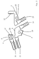
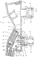
- Figures 1 and 2 show a stamped and bent part 1 or three contact elements 2, 3 and 4 on an enlarged scale of 5: 1, while Figures 3 and 4 also represent an insulating body 22 on the same scale of 5: 1.
- the one-piece stamped and bent part 1 is shown, which consists for example of hardened brass sheet with a thickness of 0.25 mm. From this sheet brass, a blank was punched according to the scheme of the connector 5, which has three openings 6, 7 and 8, which are explained elsewhere. Usually, several blanks and a carrier strip 9 are produced in one piece with the punching process, so that the individual arrangement but the entire arrangement cannot be handled during further processing. The outer dimensions of a blank including the carrier strip 9 are approximately 25 x 25 mm. From each blank three contact elements 2, 3 and 4 are then bent, which are mechanically connected by webs 10 and 11 and represent the one-piece stamped and bent part 1.
- Each contact element 2, 3 and 4 has two different types of connection points 12, 13; 14, 15 and 16, 17, which are electrically connected to one another by perforated conductor tracks 18, 19 and 20.
- the punched and bent part 1 created in this way is inserted into a tool in which the two webs 10 and 11 are separated and the carrier strip 9 is removed.
- the contact elements 2, 3 and 4 are inserted into receiving profiles 23, 24 and 25 formed in the lower housing part 21, while at the same time the openings 6, 7 and 8 interact with mandrels 26, 27 and 28 formed in the lower housing part 21.
- the fixation of the contact elements 2, 3 and 4 is ended by hot stamping the mandrels 26, 27 and 28, so that no change in position is possible. (see Figure 3)
- the insulating body 22 is made of a plastic and is composed of an upper housing part 29 and the lower housing part 21, so that the insulating body 22 has an angular outer shape when closed.
- the contact elements 2 and 4 each have a connection point 12, 17 realized as a soldering clamp contact, between which a receiving profile 30 is formed in the lower housing part 21.
- An electrical component 40 in this case a choke coil, is inserted into this receiving profile 30 after equipping the lower housing part 21 with the contact elements 2, 3 and 4, its connecting arms 41 and 42 being clamped and soldered in the connecting points 12 and 17.
- connection point 13 of the contact element 2 and the connection point 14 of the contact element 3 are parallel to each other in a housing leg 31 and are designed as box contacts. Stripped lines (not shown) of a cable set are inserted and soldered into these connection points 13 and 14.
- the connection point 15 of the contact element 3 and the connection point 16 of the contact element 4 are also parallel to one another in a housing leg 33 and are designed as solder lugs bent in their longitudinal extent.
- the connection points 15 and 16 are not yet connected with contact pins.
- the insulating body 22, including the housing legs 31, 32 and 33, has an angled outer shape in the closed state (FIG. 4).
- the housing legs 31 and 32 are located on each other and are locked via the recesses 35 and the lugs 37.
- the housing leg 33 remains without a counterpart, so that the ignition cartridge (not shown) can be contacted and soldered at the connection points 15 and 16 only immediately before the connector 5 is installed in a motor vehicle.
Landscapes
- Engineering & Computer Science (AREA)
- Manufacturing & Machinery (AREA)
- Connector Housings Or Holding Contact Members (AREA)
- Coupling Device And Connection With Printed Circuit (AREA)
- Details Of Connecting Devices For Male And Female Coupling (AREA)
- Manufacturing Of Electrical Connectors (AREA)
Applications Claiming Priority (2)
| Application Number | Priority Date | Filing Date | Title |
|---|---|---|---|
| DE19531126A DE19531126C1 (de) | 1995-08-24 | 1995-08-24 | Verfahren zur Herstellung eines elektrischen Verbinders |
| DE19531126 | 1995-08-24 |
Publications (3)
| Publication Number | Publication Date |
|---|---|
| EP0762549A2 true EP0762549A2 (fr) | 1997-03-12 |
| EP0762549A3 EP0762549A3 (fr) | 1998-06-17 |
| EP0762549B1 EP0762549B1 (fr) | 2000-08-30 |
Family
ID=7770266
Family Applications (1)
| Application Number | Title | Priority Date | Filing Date |
|---|---|---|---|
| EP96113146A Expired - Lifetime EP0762549B1 (fr) | 1995-08-24 | 1996-08-16 | Connecteur électrique |
Country Status (3)
| Country | Link |
|---|---|
| EP (1) | EP0762549B1 (fr) |
| DE (2) | DE19531126C1 (fr) |
| ES (1) | ES2149409T3 (fr) |
Cited By (1)
| Publication number | Priority date | Publication date | Assignee | Title |
|---|---|---|---|---|
| EP1555865A3 (fr) * | 2004-01-14 | 2006-01-18 | MD Elektronik GmbH | Assemblage d'un circuit bouchon avec des composants électroniques discrets et passifs |
Families Citing this family (3)
| Publication number | Priority date | Publication date | Assignee | Title |
|---|---|---|---|---|
| DE19804170A1 (de) * | 1998-02-03 | 1999-08-05 | Siemens Ag | Elektrische Baueinheit sowie Verfahren zur Herstellung einer elektrischen Baueinheit |
| DE10039623A1 (de) * | 2000-08-09 | 2002-02-28 | Falko Eidner | Elektrische Steckverbindung und Verfahren zur Herstellung |
| DE10039624A1 (de) * | 2000-08-09 | 2002-02-28 | Falko Eidner | Elektrische Steckverbindung und Verfahren zur Herstellung derselben |
Family Cites Families (11)
| Publication number | Priority date | Publication date | Assignee | Title |
|---|---|---|---|---|
| DE820915C (de) * | 1948-04-16 | 1951-11-15 | Robert Kapp | Verfahren zur Herstellung von vielteiligen elektrischen und radio-elektrischen Apparaten |
| FR2344151A1 (fr) * | 1976-03-08 | 1977-10-07 | Amp Inc | Connecteur electrique et son procede de production |
| FR2361007A1 (fr) * | 1976-08-06 | 1978-03-03 | Sev Marchal | Procede de fabrication d'un circuit electrique notamment pour un pont redresseur d'alternateur de vehicule automobile |
| DE3612576C1 (de) * | 1986-04-15 | 1987-06-19 | Preh Elektro Feinmechanik | Elektrisches Bauteil mit Kunststoffmantel und Verfahren zu dessen Herstellung |
| CH675931A5 (fr) * | 1988-03-14 | 1990-11-15 | Feller Ag | |
| US5031310A (en) * | 1988-09-29 | 1991-07-16 | Northern Telecom Limited | Method of manufacturing electrical receptacles |
| GB9225118D0 (en) * | 1992-12-01 | 1993-01-20 | Amp Gmbh | Shunted airbag connector |
| DE4303738C2 (de) * | 1993-02-03 | 2002-10-24 | Siemens Ag | Abdeckung für das mit einem Stecker versehene Ende eines Kabelbaumes |
| DE4310369C2 (de) * | 1993-03-30 | 1995-08-03 | Amphenol Tuchel Elect | Kontaktsatz für einen Steckverbinder |
| DE4445658C2 (de) * | 1994-04-15 | 1997-10-23 | Phoenix Contact Gmbh & Co | Verfahren zur Bestückung einer Grundleiste eines Steckverbinders für eine Printplatte mit Kontaktanschlüssen |
| DE4413756C1 (de) * | 1994-04-21 | 1995-07-13 | Amphenol Tuchel Elect | Gehäuse für einen Steckverbinder |
-
1995
- 1995-08-24 DE DE19531126A patent/DE19531126C1/de not_active Expired - Lifetime
-
1996
- 1996-08-16 ES ES96113146T patent/ES2149409T3/es not_active Expired - Lifetime
- 1996-08-16 EP EP96113146A patent/EP0762549B1/fr not_active Expired - Lifetime
- 1996-08-16 DE DE59605816T patent/DE59605816D1/de not_active Expired - Fee Related
Cited By (2)
| Publication number | Priority date | Publication date | Assignee | Title |
|---|---|---|---|---|
| EP1555865A3 (fr) * | 2004-01-14 | 2006-01-18 | MD Elektronik GmbH | Assemblage d'un circuit bouchon avec des composants électroniques discrets et passifs |
| US7468705B2 (en) | 2004-01-14 | 2008-12-23 | Md Elektronik Gmbh | Anti-resonant circuit arrangement |
Also Published As
| Publication number | Publication date |
|---|---|
| ES2149409T3 (es) | 2000-11-01 |
| DE59605816D1 (de) | 2000-10-05 |
| EP0762549B1 (fr) | 2000-08-30 |
| DE19531126C1 (de) | 1996-12-12 |
| EP0762549A3 (fr) | 1998-06-17 |
Similar Documents
| Publication | Publication Date | Title |
|---|---|---|
| DE69812774T2 (de) | Sammelschienenstruktur | |
| DE69513509T2 (de) | Verbesserte elektrische Verbindungsvorrichtung | |
| DE10232650B4 (de) | Elektrischer Verbindungskasten und Verfahren zur Herstellung desselben | |
| DE3912210A1 (de) | Elektrisches verteilergehaeuse und verfahren zu dessen herstellung | |
| EP0863530A2 (fr) | Panneau à circuit électrique et procédé de fabrication | |
| EP1199913A2 (fr) | Méthode de fabrication d'unités comprenant une feuille de circuit et un boítier de support | |
| EP3477781A1 (fr) | Douille enfichable pour cartes de circuits imprimés | |
| DE4310369C2 (de) | Kontaktsatz für einen Steckverbinder | |
| DE4404986A1 (de) | Einrichtung zur Kontaktierung elektrischer Leiter sowie Verfahren zur Herstellung einer derartigen Einrichtung | |
| DE102011076817B4 (de) | Leiterplatte für ein Steuergerät eines Fahrzeuggetriebes, Steuersystem für ein Fahrzeuggetriebe, und Verfahren zum Verbinden einer Leiterplatte für ein Steuergerät eines Fahrzeuggetriebes mit zumindest einer elektrischen Anschlussleitung | |
| DE19804170A1 (de) | Elektrische Baueinheit sowie Verfahren zur Herstellung einer elektrischen Baueinheit | |
| EP1734621B1 (fr) | Dispositif et méthode pour connecter électriquement un circuit électronique dans un boîtier | |
| EP0762549B1 (fr) | Connecteur électrique | |
| EP1238443B1 (fr) | Procede pour equiper un objet d'un faisceau de cables constitue d'au moins un conducteur plat et appareils electriques/electroniques connectes a celui-ci | |
| EP2548421B1 (fr) | Ensemble comportant un module électrique et/ou électronique et un support de circuit | |
| DE10038390C1 (de) | Funktionell asymmetrische Schaltungsträgeranordnung mit spiegelsymmetrischer Bauteileanordnung | |
| DE102015106518A1 (de) | Elektrisches Bauteil | |
| DE19749145A1 (de) | Elektrischer Anschlußbehälter | |
| DE19801409B4 (de) | Verfahren zur Herstellung von sich aus einem ersten und einem zweiten Verbinderteil zusammensetzenden Steckverbindern | |
| WO2003055008A1 (fr) | Element de contact electrique | |
| EP3216329B1 (fr) | Procédé de fabrication d'un ensemble comprenant une pièce de boîtier et au moins deux rubans conducteurs | |
| DE10209524B4 (de) | Elektrische Verkabelungsvorrichtung | |
| DE102023129565B4 (de) | Leiterplattenadapter zur kompakten und direkten elektrischen Kontaktierung von Leitern mit einer Leiterplatte | |
| EP0950271B1 (fr) | Piece pour la mise en contact d'une unite de mesure et procede de production de ladite piece | |
| DE29508805U1 (de) | Mehrpoliger elektrischer Steckverbinder |
Legal Events
| Date | Code | Title | Description |
|---|---|---|---|
| PUAI | Public reference made under article 153(3) epc to a published international application that has entered the european phase |
Free format text: ORIGINAL CODE: 0009012 |
|
| AK | Designated contracting states |
Kind code of ref document: A2 Designated state(s): DE ES FR GB IT |
|
| PUAL | Search report despatched |
Free format text: ORIGINAL CODE: 0009013 |
|
| AK | Designated contracting states |
Kind code of ref document: A3 Designated state(s): DE ES FR GB IT |
|
| RHK1 | Main classification (correction) |
Ipc: H01R 43/16 |
|
| 17P | Request for examination filed |
Effective date: 19981217 |
|
| GRAG | Despatch of communication of intention to grant |
Free format text: ORIGINAL CODE: EPIDOS AGRA |
|
| 17Q | First examination report despatched |
Effective date: 19991117 |
|
| GRAG | Despatch of communication of intention to grant |
Free format text: ORIGINAL CODE: EPIDOS AGRA |
|
| GRAH | Despatch of communication of intention to grant a patent |
Free format text: ORIGINAL CODE: EPIDOS IGRA |
|
| GRAH | Despatch of communication of intention to grant a patent |
Free format text: ORIGINAL CODE: EPIDOS IGRA |
|
| GRAA | (expected) grant |
Free format text: ORIGINAL CODE: 0009210 |
|
| ITF | It: translation for a ep patent filed | ||
| AK | Designated contracting states |
Kind code of ref document: B1 Designated state(s): DE ES FR GB IT |
|
| GBT | Gb: translation of ep patent filed (gb section 77(6)(a)/1977) |
Effective date: 20000831 |
|
| REF | Corresponds to: |
Ref document number: 59605816 Country of ref document: DE Date of ref document: 20001005 |
|
| ET | Fr: translation filed | ||
| REG | Reference to a national code |
Ref country code: ES Ref legal event code: FG2A Ref document number: 2149409 Country of ref document: ES Kind code of ref document: T3 |
|
| PLBE | No opposition filed within time limit |
Free format text: ORIGINAL CODE: 0009261 |
|
| STAA | Information on the status of an ep patent application or granted ep patent |
Free format text: STATUS: NO OPPOSITION FILED WITHIN TIME LIMIT |
|
| 26N | No opposition filed | ||
| REG | Reference to a national code |
Ref country code: GB Ref legal event code: IF02 |
|
| PGFP | Annual fee paid to national office [announced via postgrant information from national office to epo] |
Ref country code: ES Payment date: 20030829 Year of fee payment: 8 |
|
| PGFP | Annual fee paid to national office [announced via postgrant information from national office to epo] |
Ref country code: GB Payment date: 20030901 Year of fee payment: 8 |
|
| PG25 | Lapsed in a contracting state [announced via postgrant information from national office to epo] |
Ref country code: GB Free format text: LAPSE BECAUSE OF NON-PAYMENT OF DUE FEES Effective date: 20040816 |
|
| PG25 | Lapsed in a contracting state [announced via postgrant information from national office to epo] |
Ref country code: ES Free format text: LAPSE BECAUSE OF NON-PAYMENT OF DUE FEES Effective date: 20040817 |
|
| GBPC | Gb: european patent ceased through non-payment of renewal fee |
Effective date: 20040816 |
|
| PGFP | Annual fee paid to national office [announced via postgrant information from national office to epo] |
Ref country code: FR Payment date: 20050809 Year of fee payment: 10 |
|
| PGFP | Annual fee paid to national office [announced via postgrant information from national office to epo] |
Ref country code: DE Payment date: 20050811 Year of fee payment: 10 |
|
| REG | Reference to a national code |
Ref country code: ES Ref legal event code: FD2A Effective date: 20040817 |
|
| PGFP | Annual fee paid to national office [announced via postgrant information from national office to epo] |
Ref country code: IT Payment date: 20060831 Year of fee payment: 11 |
|
| PG25 | Lapsed in a contracting state [announced via postgrant information from national office to epo] |
Ref country code: DE Free format text: LAPSE BECAUSE OF NON-PAYMENT OF DUE FEES Effective date: 20070301 |
|
| REG | Reference to a national code |
Ref country code: FR Ref legal event code: ST Effective date: 20070430 |
|
| PG25 | Lapsed in a contracting state [announced via postgrant information from national office to epo] |
Ref country code: FR Free format text: LAPSE BECAUSE OF NON-PAYMENT OF DUE FEES Effective date: 20060831 |
|
| PG25 | Lapsed in a contracting state [announced via postgrant information from national office to epo] |
Ref country code: IT Free format text: LAPSE BECAUSE OF NON-PAYMENT OF DUE FEES Effective date: 20070816 |