EP0762818A2 - Dispositif pour réaliser une connexion à une plaquette de circuit - Google Patents
Dispositif pour réaliser une connexion à une plaquette de circuit Download PDFInfo
- Publication number
- EP0762818A2 EP0762818A2 EP96114209A EP96114209A EP0762818A2 EP 0762818 A2 EP0762818 A2 EP 0762818A2 EP 96114209 A EP96114209 A EP 96114209A EP 96114209 A EP96114209 A EP 96114209A EP 0762818 A2 EP0762818 A2 EP 0762818A2
- Authority
- EP
- European Patent Office
- Prior art keywords
- circuit board
- counter bearing
- carrier
- pad
- printed circuit
- Prior art date
- Legal status (The legal status is an assumption and is not a legal conclusion. Google has not performed a legal analysis and makes no representation as to the accuracy of the status listed.)
- Withdrawn
Links
Images

Classifications
-
- H—ELECTRICITY
- H05—ELECTRIC TECHNIQUES NOT OTHERWISE PROVIDED FOR
- H05K—PRINTED CIRCUITS; CASINGS OR CONSTRUCTIONAL DETAILS OF ELECTRIC APPARATUS; MANUFACTURE OF ASSEMBLAGES OF ELECTRICAL COMPONENTS
- H05K7/00—Constructional details common to different types of electric apparatus
- H05K7/14—Mounting supporting structure in casing or on frame or rack
- H05K7/1438—Back panels or connecting means therefor; Terminals; Coding means to avoid wrong insertion
- H05K7/1439—Back panel mother boards
-
- H—ELECTRICITY
- H05—ELECTRIC TECHNIQUES NOT OTHERWISE PROVIDED FOR
- H05K—PRINTED CIRCUITS; CASINGS OR CONSTRUCTIONAL DETAILS OF ELECTRIC APPARATUS; MANUFACTURE OF ASSEMBLAGES OF ELECTRICAL COMPONENTS
- H05K7/00—Constructional details common to different types of electric apparatus
- H05K7/14—Mounting supporting structure in casing or on frame or rack
Definitions
- the invention relates to a device for producing an electrical connection.
- a plug connection can meet these requirements, it requires a locking device for moving and releasing the parts of the plug connection. Such a device ensures that all contacts are closed and, on the other hand, that these contacts do not come loose during operation.
- EP 03 69 025 a device is described with which cards can be connected to the circuit board and released again.
- the device consists of an elastic locking part which is connected to the card, the locking part having a movable end part and an operating lever which is rotatably mounted on the card.
- the operating lever and the locking part are arranged with respect to one another such that when the operating lever is rotated, the locking part performs a translatory movement due to the curved surface of the operating lever, as a result of which a connection is established between the card and the circuit board.
- the movable end part falls into a groove provided on the operating lever and remains in this position, as a result of which the card is fixed in this position.
- a disadvantage of this device is, in particular, that the pressure exerted by the pushing-in force constantly rests on the circuit board, so that the circuit board is under high tension during connection to the card. In addition, it cannot be ruled out that the insertion force is so great due to the many contacts that have to be made by the plug connection that the circuit board bends. A permanent bending of the board leads to cracks on the board, so that the printed lines are destroyed.
- Another disadvantage of this device results from the fact that, due to the aforementioned problems, the number of contacts that can be made by a plug connection is limited, i.e. that large cards with a large number of contacts cannot be locked with this device. The functions must therefore be distributed over several cards, which leads to larger housings.
- a device of the type mentioned above for locking and releasing a connection for electrical plug contacts is in the IBM Technical Disclosure Bulletin, Vol. 31, No. 11, April 1989, pp. 76-80.
- This device consists of locking levers, which are arranged at the upper and lower corner of the card or the protective housing, and locks, which are attached to the housing.
- a lock is functionally assigned to each locking lever such that the locking lever can only come into engagement with the lock when an effective connection between the card and the circuit board has been established.
- a major disadvantage of this device is that the pressure required to connect the card to the board is on the parts of the connector during operation. Otherwise, this device has the same disadvantages that were listed in European application EP 03 69 025.
- DE 4042060 C1 discloses a device for connecting and disconnecting an electrical plug connection.
- the device consists of locking levers which are rotatably arranged on the lower and upper corner area of a protective housing or a card, and flexibly designed parts, in particular springs, which are either attached to an inflexible locking part or directly to the housing. There is a driver part on the flexible parts.
- the known devices have the disadvantage in common that only a relatively limited number of connections can be made with them.
- the problem arises in particular in the case of plug-in connections that the insertion force to be applied increases with an increasing number of contact pins.
- the push-in force must not exceed a permissible maximum in order to avoid damage to the printed circuit boards and also in order to save an expensive mechanical construction for applying the necessary push-in force.
- the maximum number of connections that can be produced with the device known from DE 40 42 060 is 600 connections for a printed circuit board.
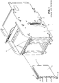
- FIG. 1 shows such a device known from DE 40 42 060.
- one or more cards 3 are inserted in parallel into a housing 1 and connected to a circuit board 5 within the housing 1.
- the cards 3, particularly if they are electronic cards, are usually stored in a protective housing 6 for protection against electromagnetic radiation.
- This protective housing 6 is designed so that it has an opening from which a contact connection part 4 protrudes, which is connected to a contact connection part 7 of the circuit board 5.
- the housing 1 there are locks 11 in the upper and lower areas, into which the latching levers 9 can only engage when an effective connection has been established between the contact connection part 7 of the circuit board 5 and the contact connection part 4 of the card 3.
- the locks 11 can be attached individually or together to a part, attached to the housing 1.
- the contact connection part 4 can be a so-called 600-pin connector, for example.
- An increase in the number of pins beyond 600 would require an excessive plug-in force which would no longer be able to be applied by muscle strength and which could also damage the card 3 or its housing 6.
- the invention is therefore based on the object of providing a device for producing a connection which makes it possible to produce a larger number of connections between a printed circuit board and a carrier printed circuit board.
- pad-on-pad connectors are used in the device according to the invention. With pad-on-pad connectors, the electrical contact is made via a contact surface, whereas with conventional pin-and-hole technology, it is necessary to insert a contact pin into an appropriate connector.
- Pad-on-pad connectors as such are known from the prior art for so-called module packaging and for connecting cables (IBM TDB Vol. 37, No. 11, November 1994, pages 581-584, IBM Research Disclosure, No. 346, February 1993, JL Rice and FH Smith, TDB No. 6, November 1992, pages 259-260 and TDB March 1985, pages 5962-5965 and TDB No. 6, November 1992, pages 259-260).
- pad-on-pad connectors minimizes the insertion force required to establish a connection between a circuit card and a carrier circuit board. This is mainly due to the fact that the friction of the contact pins when inserting into the mating connector is eliminated.
- the number of connections that can be made between a printed circuit board and a carrier printed circuit board is therefore not limited to about 600, as in the prior art, due to the frictional forces, but can also be, for example, 1,800 connections for signal transmission.
- circuit boards and carrier circuit boards that are equipped with a device according to the invention can have the same size as circuit boards equipped with pin-and-hole connectors, although the circuit cards according to the invention, for. B. have a double number of signal outputs.
- the printed circuit boards according to the invention can therefore be constructed so that they are compatible with the mechanical structure shown in FIG. 1.
- a counter bearing which is curved in the form of a circular arc for pressing the carrier circuit board onto the circuit board. If the curvature of the counterbearing is selected according to the elasticity of the material of the counterbearing and the contact pressure, the counter bearing deforms when a contact pressure is introduced so that the counter bearing bears against the carrier circuit board along its entire length. Then a particularly secure contact of the circuit board and the carrier circuit board is ensured via the pad-on-pad connectors.
- the counter bearing can be suspended on the carrier circuit board with play using elastic elements. That proves is advantageous when adjusting the circuit board and the carrier circuit board during insertion. This supports self-adjustment.
- Another advantage of the elastic suspension is the shock absorption when transporting the carrier circuit board with the built-in circuit board. This reduces the mechanical load on the printed circuit board and thus also on the carrier printed circuit board.
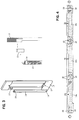
- a circuit card 12 is shown in FIG. 2, which has a pad-on-pad connector 14.
- the counterpart to the pad-on-pad connector 14 is located on the carrier circuit board 13.
- the carrier circuit board 13 corresponds to the circuit board 5 of FIG. 1, which however only has pin-and-hole connectors.
- the card 6 is contacted on the carrier circuit board 13 - as is known from the prior art - by means of a pin-and-hole connector.
- connection between the circuit card 12 and the carrier circuit card 13 is established according to the invention by a pad-on-pad connector 14.
- the pad-on-pad connector 14 consists of a total of 3 individual connectors arranged next to one another (cf. FIG. 4).
- the connector 14 and its counterpart located on the carrier circuit board 13 are pressed together by means of the screws 16 in order to ensure reliable contacting.
- a pressure force is introduced by the screws 16 into the counter bearing 15 located on the carrier circuit board 13 (cf. FIG. 3).
- the mechanical structure corresponds to the structure shown in FIG. 1.
- the individual printed circuit boards 12 also have locking levers 9.
- the counter bearing 15 is fixed in the assembled state on the carrier circuit board 13 by means of elastic elements 17.
- the elastic elements 17 can be made of plastic, for example.
- the counter bearing 15 is curved in a circular arc. The radius of the circular arc is much larger than its length. The center of the circle lies on the side facing away from the printed circuit board 12.
- the bores 18 in the counter bearing 15 are provided with an internal thread.
- the circuit board 12 is first inserted into a housing which corresponds to the housing 1 in FIG. 1.
- the circuit board 12 is pre-adjusted with respect to the carrier circuit board 13.
- the screws 16 are screwed into the holes 18 in the counter bearing 15.
- a contact pressure is thereby introduced into the counter bearing 15.
- the pad-on-pad connector 14 is finely adjusted with respect to its counterpart on the carrier circuit board 13 during screwing.
- the preliminary and fine adjustment supported by the conical elements 19 and 20 (Fig. 4).
- the conical elements 19 and 20 are located on the individual connectors 14a, 14b, 14c.
- the elements 19 and 20 are cylindrical with a truncated cone attachment, that is to say shaped like a beveled bolt.
- the elements 19 are kept floating so that they can move sideways.
- the elements 20, however, are fixedly attached to the individual connectors 14a, 14b, 14c.
- the individual connectors 14a, 14b, 14c correspond to connectors on the carrier circuit board 13, via which the signal connections are made.
- FIG. 4 therefore quasi shows a footprint of the corresponding connectors of the carrier circuit board 13.
- the conical elements 19 are inserted into receiving bores in the carrier circuit board 13. This is facilitated by the lateral play of the elements 19.
- the connectors 14a, 14b, 14c are pre-adjusted to their corresponding counterparts. The fine adjustment then takes place when the elements 20 are introduced into their corresponding receiving bores. This occurs after the pre-adjustment, since the elements 20 have a smaller height expansion than the elements 19.
Landscapes
- Engineering & Computer Science (AREA)
- Microelectronics & Electronic Packaging (AREA)
- Coupling Device And Connection With Printed Circuit (AREA)
Applications Claiming Priority (2)
| Application Number | Priority Date | Filing Date | Title |
|---|---|---|---|
| DE19533569 | 1995-09-11 | ||
| DE1995133569 DE19533569C2 (de) | 1995-09-11 | 1995-09-11 | Vorrichtung zur Herstellung einer Verbindung mit einer Leiterplatte |
Publications (2)
| Publication Number | Publication Date |
|---|---|
| EP0762818A2 true EP0762818A2 (fr) | 1997-03-12 |
| EP0762818A3 EP0762818A3 (fr) | 1997-05-14 |
Family
ID=7771838
Family Applications (1)
| Application Number | Title | Priority Date | Filing Date |
|---|---|---|---|
| EP96114209A Withdrawn EP0762818A3 (fr) | 1995-09-11 | 1996-09-05 | Dispositif pour réaliser une connexion à une plaquette de circuit |
Country Status (3)
| Country | Link |
|---|---|
| EP (1) | EP0762818A3 (fr) |
| JP (1) | JPH09115622A (fr) |
| DE (1) | DE19533569C2 (fr) |
Families Citing this family (2)
| Publication number | Priority date | Publication date | Assignee | Title |
|---|---|---|---|---|
| DE20117188U1 (de) | 2001-10-19 | 2002-01-03 | STOCKO Contact GmbH & Co. KG, 42327 Wuppertal | Adapter zum Kontaktieren von Chipkarten |
| DE102016118630B3 (de) | 2016-09-30 | 2018-02-22 | Fujitsu Limited | Computersystem |
Family Cites Families (10)
| Publication number | Priority date | Publication date | Assignee | Title |
|---|---|---|---|---|
| US2993187A (en) * | 1960-06-29 | 1961-07-18 | South Chester Corp | Module board fastener |
| DE3507482A1 (de) * | 1985-03-02 | 1986-09-04 | Telefonbau Und Normalzeit Gmbh, 6000 Frankfurt | Andruckverbindersystem fuer mehrlagenleiterplatten |
| EP0369025B1 (fr) * | 1988-04-30 | 1994-06-22 | Fujitsu Limited | Mecanisme d'insertion et de retrait d'unites de cartes imprimees pour dispositifs a circuits electroniques |
| DE3917527A1 (de) * | 1989-05-30 | 1990-12-06 | Kloeckner Becorit Gmbh | Steuergeraet, insbesondere fuer die elektrohydraulische steuerung eines grubenausbaugestelles |
| ATE105458T1 (de) * | 1990-08-03 | 1994-05-15 | Siemens Nixdorf Inf Syst | Einbausystem fuer elektrische funktionseinheiten insbesondere fuer die datentechnik. |
| DE4042060C1 (fr) * | 1990-12-28 | 1992-06-25 | International Business Machines Corp., Armonk, N.Y., Us | |
| JPH0746618B2 (ja) * | 1991-07-30 | 1995-05-17 | インターナショナル・ビジネス・マシーンズ・コーポレイション | 回路接続装置およびそれを使用する電気回路システム |
| US5161986A (en) * | 1991-10-15 | 1992-11-10 | Ceridian Corporation | Low inductance circuit apparatus with controlled impedance cross-unders and connector for connecting to backpanels |
| US5254016A (en) * | 1992-06-17 | 1993-10-19 | Compaq Computer Corporation | Interconnect device mounting apparatus for printed circuit boards |
| US5395249A (en) * | 1993-06-01 | 1995-03-07 | Westinghouse Electric Corporation | Solder-free backplane connector |
-
1995
- 1995-09-11 DE DE1995133569 patent/DE19533569C2/de not_active Expired - Fee Related
-
1996
- 1996-09-04 JP JP8234548A patent/JPH09115622A/ja active Pending
- 1996-09-05 EP EP96114209A patent/EP0762818A3/fr not_active Withdrawn
Also Published As
| Publication number | Publication date |
|---|---|
| EP0762818A3 (fr) | 1997-05-14 |
| DE19533569A1 (de) | 1997-03-13 |
| DE19533569C2 (de) | 1997-08-07 |
| JPH09115622A (ja) | 1997-05-02 |
Similar Documents
| Publication | Publication Date | Title |
|---|---|---|
| DE68915973T2 (de) | Elektrischer Verbinder unter Verwendung einer Leiterplatte. | |
| DE3887872T2 (de) | Verriegelungssystem. | |
| DE19654206A1 (de) | Computer-System mit leicht erweiterbaren Funktionen | |
| DE3537400A1 (de) | Gehaeuse fuer eine erweiterbare periphere interface-einheit | |
| DE10133662B4 (de) | Steckverbinder zur Verbindung mit einer Leiterplatte | |
| EP0260425A1 (fr) | Dispositif de soulagement de la traction | |
| EP1245933A2 (fr) | Dispositif électromécanique pour le montage d' un équipement électronique sur un support, en particulier pour le montage d' un instrument indicateur encastré dans un tableau de bord | |
| EP2481126A1 (fr) | Broche à pression à branches multiples | |
| DE69104310T2 (de) | Elektrischer verbinder für prüfstand. | |
| EP2240004B1 (fr) | Aide au montage pour connecteur enfichable de cartes de circuits imprimés | |
| DE4437316A1 (de) | Dezentrale Ein/Ausgabebaugruppe für elektronische Steuerungen | |
| EP3493333A1 (fr) | Fiche de raccordement électrique destinée à la transmission de données | |
| DE2912740A1 (de) | Vorrichtung zum entriegeln und herausziehen fuer eine elektrische verbindung sowie mit einer derartigen vorrichtung ausgeruestete elektrische verbindung | |
| DE69112005T2 (de) | Vorrichtung zum Stecken und Ziehen eines elektrischen Verbinders. | |
| DE69307103T2 (de) | Verfahren zur Befestigung eines beweglichen auf einen festen Verbinder und Befestigungsteil dafür | |
| EP2077704A1 (fr) | Module électronique enfichable destiné à la réception dans un support de composants | |
| DE69017250T2 (de) | Gerät zur nacheinanderfolgenden Verbindung von elektrischen Leiterplatten. | |
| EP1237395B1 (fr) | Assemblage de panneaux à circuit imprimé | |
| WO2007110053A2 (fr) | Fond de panier pour un support de modules électronique | |
| EP1264369A1 (fr) | Connexion par enfichage | |
| EP1929848B1 (fr) | Connexion de deux cartes de circuits imprimes ou de modules plats au moyen d'un systeme de verrouillage mecanique | |
| DE102016118630B3 (de) | Computersystem | |
| DE19533569C2 (de) | Vorrichtung zur Herstellung einer Verbindung mit einer Leiterplatte | |
| EP2689496B1 (fr) | Élément d'enfichage direct, en particulier pour appareils de commande de véhicule | |
| EP0784354A2 (fr) | Serre-câble de courant fort pour un assemblage de plaque à circuit |
Legal Events
| Date | Code | Title | Description |
|---|---|---|---|
| PUAI | Public reference made under article 153(3) epc to a published international application that has entered the european phase |
Free format text: ORIGINAL CODE: 0009012 |
|
| AK | Designated contracting states |
Kind code of ref document: A2 Designated state(s): DE FR GB |
|
| PUAL | Search report despatched |
Free format text: ORIGINAL CODE: 0009013 |
|
| AK | Designated contracting states |
Kind code of ref document: A3 Designated state(s): DE FR GB |
|
| STAA | Information on the status of an ep patent application or granted ep patent |
Free format text: STATUS: THE APPLICATION IS DEEMED TO BE WITHDRAWN |
|
| 18D | Application deemed to be withdrawn |
Effective date: 19971115 |