EP0763832A1 - Bistabiles magnetisches Element und Verfahren zu seiner Herstellung - Google Patents
Bistabiles magnetisches Element und Verfahren zu seiner Herstellung Download PDFInfo
- Publication number
- EP0763832A1 EP0763832A1 EP96114631A EP96114631A EP0763832A1 EP 0763832 A1 EP0763832 A1 EP 0763832A1 EP 96114631 A EP96114631 A EP 96114631A EP 96114631 A EP96114631 A EP 96114631A EP 0763832 A1 EP0763832 A1 EP 0763832A1
- Authority
- EP
- European Patent Office
- Prior art keywords
- wire
- bistable
- magnetic
- magnetic element
- magnetic material
- Prior art date
- Legal status (The legal status is an assumption and is not a legal conclusion. Google has not performed a legal analysis and makes no representation as to the accuracy of the status listed.)
- Granted
Links
Images


Classifications
-
- G—PHYSICS
- G11—INFORMATION STORAGE
- G11C—STATIC STORES
- G11C11/00—Digital stores characterised by the use of particular electric or magnetic storage elements; Storage elements therefor
- G11C11/02—Digital stores characterised by the use of particular electric or magnetic storage elements; Storage elements therefor using magnetic elements
- G11C11/14—Digital stores characterised by the use of particular electric or magnetic storage elements; Storage elements therefor using magnetic elements using thin-film elements
- G11C11/155—Digital stores characterised by the use of particular electric or magnetic storage elements; Storage elements therefor using magnetic elements using thin-film elements with cylindrical configuration
-
- G—PHYSICS
- G01—MEASURING; TESTING
- G01R—MEASURING ELECTRIC VARIABLES; MEASURING MAGNETIC VARIABLES
- G01R33/00—Arrangements or instruments for measuring magnetic variables
- G01R33/02—Measuring direction or magnitude of magnetic fields or magnetic flux
-
- G—PHYSICS
- G11—INFORMATION STORAGE
- G11C—STATIC STORES
- G11C11/00—Digital stores characterised by the use of particular electric or magnetic storage elements; Storage elements therefor
- G11C11/02—Digital stores characterised by the use of particular electric or magnetic storage elements; Storage elements therefor using magnetic elements
- G11C11/14—Digital stores characterised by the use of particular electric or magnetic storage elements; Storage elements therefor using magnetic elements using thin-film elements
-
- H—ELECTRICITY
- H01—ELECTRIC ELEMENTS
- H01F—MAGNETS; INDUCTANCES; TRANSFORMERS; SELECTION OF MATERIALS FOR THEIR MAGNETIC PROPERTIES
- H01F1/00—Magnets or magnetic bodies characterised by the magnetic materials therefor; Selection of materials for their magnetic properties
- H01F1/01—Magnets or magnetic bodies characterised by the magnetic materials therefor; Selection of materials for their magnetic properties of inorganic materials
- H01F1/03—Magnets or magnetic bodies characterised by the magnetic materials therefor; Selection of materials for their magnetic properties of inorganic materials characterised by their coercivity
- H01F1/0302—Magnets or magnetic bodies characterised by the magnetic materials therefor; Selection of materials for their magnetic properties of inorganic materials characterised by their coercivity characterised by unspecified or heterogeneous hardness or specially adapted for magnetic hardness transitions
- H01F1/0304—Magnets or magnetic bodies characterised by the magnetic materials therefor; Selection of materials for their magnetic properties of inorganic materials characterised by their coercivity characterised by unspecified or heterogeneous hardness or specially adapted for magnetic hardness transitions adapted for large Barkhausen jumps or domain wall rotations, e.g. WIEGAND or MATTEUCCI effect
-
- H—ELECTRICITY
- H01—ELECTRIC ELEMENTS
- H01F—MAGNETS; INDUCTANCES; TRANSFORMERS; SELECTION OF MATERIALS FOR THEIR MAGNETIC PROPERTIES
- H01F1/00—Magnets or magnetic bodies characterised by the magnetic materials therefor; Selection of materials for their magnetic properties
- H01F1/01—Magnets or magnetic bodies characterised by the magnetic materials therefor; Selection of materials for their magnetic properties of inorganic materials
- H01F1/03—Magnets or magnetic bodies characterised by the magnetic materials therefor; Selection of materials for their magnetic properties of inorganic materials characterised by their coercivity
- H01F1/12—Magnets or magnetic bodies characterised by the magnetic materials therefor; Selection of materials for their magnetic properties of inorganic materials characterised by their coercivity of soft-magnetic materials
- H01F1/14—Magnets or magnetic bodies characterised by the magnetic materials therefor; Selection of materials for their magnetic properties of inorganic materials characterised by their coercivity of soft-magnetic materials metals or alloys
- H01F1/147—Alloys characterised by their composition
- H01F1/153—Amorphous metallic alloys, e.g. glassy metals
- H01F1/15391—Elongated structures, e.g. wires
-
- H—ELECTRICITY
- H01—ELECTRIC ELEMENTS
- H01F—MAGNETS; INDUCTANCES; TRANSFORMERS; SELECTION OF MATERIALS FOR THEIR MAGNETIC PROPERTIES
- H01F10/00—Thin magnetic films, e.g. of one-domain structure
- H01F10/08—Thin magnetic films, e.g. of one-domain structure characterised by magnetic layers
- H01F10/10—Thin magnetic films, e.g. of one-domain structure characterised by magnetic layers characterised by the composition
- H01F10/12—Thin magnetic films, e.g. of one-domain structure characterised by magnetic layers characterised by the composition being metals or alloys
- H01F10/13—Amorphous metallic alloys, e.g. glassy metals
- H01F10/132—Amorphous metallic alloys, e.g. glassy metals containing cobalt
Definitions
- the present invention relates to a bistable magnetic element which is compact and has high sensitivity and high response speed and a method of manufacturing such a bistable magnetic element.
- the bistable magnetic element of the present invention is suitable for use in magnetic sensor switches such as a proximity switch and a digital magnetic switch which are used in input devices for computers and information equipment and in equipment for factory automation (FA), and is also suitable for use in digital magnetic memory cells and the like for computers and information equipment which allow high speed read/write operation.
- micro-sized digital memory cell which has high sensitivity and high response speed and which has a simple shape and a desired sensor function.
- magnetic elements which satisfy the above-described requirements have not yet been developed.
- a parametron element was used as a nondestructive magnetic memory.
- the rise time of parametric excitation upon reception of a trigger pulse is long (i.e., a few microseconds), and coils are required, which makes it difficult to fabricate the parametron element as a part of an integrated circuit. Accordingly, the parametron element is not used in these days.
- twistor memory element in which electrically conductive permalloy foil is wound helically has been invented.
- the twistor memory element operates as a bistable magnetic memory, the manufacture thereof is troublesome, and it is necessary to supply a large current to the memory element.
- the twistor memory element is also difficult to fabricate as a part of an integrated circuit. Due to these drawbacks, the twistor memory element is not used in these days.
- a huge number of magnetic type proximity switches are used in keyboards and mice for computers and word processors, joy sticks for game machines, and proximity sensors for FA.
- a combination module of a Hall element or MR element and a hysteresis comparator used in the magnetic proximity switches requires a magnetic field of a few tens gausses or higher to operate, which means that the sensitivity of the module is low.
- the temperature characteristics of the module is not stable.
- a head including a fluxgate sensor can be used to obtain high sensitivity.
- the size of the head cannot be reduced.
- the response speed of the head is low because the head is excited by coil current.
- An object of the present invention is to solve the above-mentioned problems and to provide a bistable magnetic element which is compact and which has high sensitivity and high response speed.
- Another object of the present invention is to provide a method of manufacturing the bistable magnetic element as set forth above.
- the present invention provides a bistable magnetic element, in which a pulse current or a dc-biased high frequency current is supplied to a soft magnetic material having a helical magnetic anisotropy.
- a pulse current or a dc-biased high frequency current is supplied to a soft magnetic material having a helical magnetic anisotropy.
- bistable magnetic element which has high sensitivity and high response speed.
- the soft magnetic material is an amorphous magnetic material.
- the impedance can be increased and the size of the bistable magnetic element can be decreased further.
- the amorphous magnetic material is an amorphous wire.
- the size of the bistable magnetic element can be decreased further to the order of less than one millimeter, and it is possible to obtain large voltage variations with respect to variations in external magnetic fields.
- the soft magnetic material is a thin film.
- the size of the bistable magnetic element can be decreased further to the order of less than one millimeter, and it is possible to obtain large voltage variations with respect to variations in external magnetic fields.
- the present invention also provides a method of manufacturing a bistable magnetic element.
- This method includes the steps of drawing an elongated soft magnetic material having a magnetostriction as to obtain a thin wire; annealing the wire while applying a tension thereto; twisting the wire by a predetermined amount; and fixing both ends of the wire to electrodes.
- a twist stress is applied to the wire so as to induce helical magnetic anisotropy utilizing the inverse magnetostrictive effect. Accordingly, it is possible to easily manufacture a bistable magnetic element which is compact and which has high sensitivity and high response speed.
- the soft magnetic material wire is preferably an amorphous wire having a composition of FeCoSiB.
- the present invention also provides a method of manufacturing a bistable magnetic element.
- This method includes the steps of drawing an elongated soft magnetic material having a magnetostriction as to obtain a thin wire; annealing the wire in a state in which the wire has been twisted by a predetermined amount; quenching the wire; and fixing both ends of the wire to electrodes.
- the wire is heated and quenched in a state in which a twist stress has been applied to the wire so as to induce helical magnetic anisotropy. Accordingly, it is possible to easily manufacture a bistable magnetic element which is compact and which has high sensitivity and high response speed.
- the soft magnetic material wire is preferably an amorphous wire having a composition of CoSiB.
- the present invention also provides a method of manufacturing a bistable magnetic element.
- This method includes the steps of forming an elongated thin film of a soft magnetic material having zero magnetostriction; annealing the thin film in a state in which a circulating dc magnetic field and a longitudinal dc magnetic field are simultaneously applied to the thin film; and fixing both ends of the annealed thin film to electrodes.
- helical magnetic anisotropy is induced by a so-called “orthogonal magnetic field annealing method" in which annealing is performed in a state in which a dc current (i.e., circulating dc magnetic field) and a longitudinal dc magnetic field are simultaneously applied to the thin film. Accordingly, it is possible to easily manufacture a bistable magnetic element which is compact and which has high sensitivity and high response speed.
- an amorphous sputtered thin film having a composition of FeCoB is preferably used as the thin film of the soft magnetic material.
- the present invention provides a micro-sized bistable magnetic element which has high sensitivity and high response speed.
- the bistable magnetic element utilizes an elongated soft magnetic material having a high permeability in which helical magnetic anisotropy has been induced.
- An external magnetic field is applied to the magnetic material in the longitudinal direction thereof, so that bistable magnetic operation is caused by a jumping hysteresis phenomenon of the magnetization rotation.
- a sharp pulse current or a dc-biased high frequency current is supplied to the magnetic material, a large voltage variation is induced between opposite ends of the magnetic material in accordance with the bistable magnetization due to high speed magnetization rotation.
- FIG. 1 is a circuit diagram showing the structure of a bistable magnetic element according to the present invention.
- a high frequency power supply (e ac )2 and a direct current power supply (E dc ) (or a pulse generator) 3 are connected to a soft magnetic material (amorphous wire) 1 having helical magnetic anisotropy via a resistor (R) 4, thereby supplying to the soft magnetic material 1 a high frequency current on which a direct current or a pulse current is superposed.
- a resistor (R) 4 thereby supplying to the soft magnetic material 1 a high frequency current on which a direct current or a pulse current is superposed.
- the magnetic material no limitation is imposed on the magnetic material, provided that it has helical magnetic anisotropy.
- the magnetic material has an elongated shape, it is possible to reduce the size and to obtain increased variations in the output voltage.
- the impedance of the magnetic material can be increased because of its large electrical resistivity. This makes it possible to reduce the size further, and to obtain further increased variations in the output voltage.
- twist stress is applied to the wire to utilize the inverse magnetostrictive effect, or a so-called “twist annealing method" is used in which heating and quenching are performed in a state in which a twist stress has been applied to the wire, thereby inducing the helical magnetic anisotropy.
- a so-called “transverse magnetic field annealing method” is used in which annealing is performed in a state in which a direct current (i.e., circulated dc magnetic field) and a dc magnetic field are simultaneously applied to the thin film in the longitudinal direction thereof.
- the helical anisotropy is induced only in the surface layer of the magnetic material.
- these inducing methods are sufficiently effective, because induction of a voltage depends only on the magnetic characteristic of the surface layer due to the skin effect of a pulse current or a high frequency current.
- the above-described bistable magnetic element is manufactured as follows.
- An amorphous wire (diameter: 30 ⁇ m, length: 1 mm, zero magnetostriction) is twisted, and both ends of the wire are soldered to electrodes.
- a sharp pulse current having a pulse width of about 5 ns and a height of about 15 mA is supplied to the wire, the wire exhibits a clear bistable operation in response to application of magnetic fields of about ⁇ 1 gauss (or oersted) in the longitudinal direction of the wire.
- the magnitudes of the memory voltage pulses are about 200 mV and about 400 mV.
- thin wire having a high permeability such as wire made of amorphous material or made of permalloy or wire of silicon steel may be used.
- Two methods are generally used to realize a bistable element using a magnetic material.
- flux reversal due to domain wall propagation is utilized.
- flux reversal due to rotation of the magnetization vector is utilized.
- Amorphous wire is widely used in security sensor tags.
- this domain wall propagation type bistable magnetic element a sharp pulse (pulse width at the half amplitude: several micro seconds) is induced in a detection coil (in the case of a twisted wire, in the detection coil or between both ends of the wire) regardless of the excitation frequency (0.01 - 50 kHz) of an external magnetic field.
- the bistable magnetic element in order to avoid the effect of the demagnetizing field, the bistable magnetic element must have a length corresponding to the length of the domain wall.
- the wire In the case of a tension-annealed amorphous wire, the wire must have a length of 10 mm or greater after being drawn.
- the wire In the case of an as-cast wire, the wire must have a length of 80 mm or greater after being drawn.
- the following techniques are employed to provide a highly sensitive bistable magnetic element. That is, in order to meet the requirement (i), a high frequency current or a very sharp pulse current is applied to a magnetic material, so that domain walls are prevented from moving by a strong suppressing force generated by eddy current. In order to meet the requirement (ii), a twist stress is applied to the magnetic wire so as to induce helical magnetic anisotropy in the surface layer of the wire utilizing the reverse effect of the magnetostriction such that the helical magnetic anisotropy is induced with an angle of about ⁇ 45° with respect to the longitudinal axis of the wire.
- These techniques make it possible to provide a highly sensitive bistable magnetic element which has a very small length of about 1 mm, which has a considerably high response speed (several nano seconds), and which has a small threshold magnetic field of about 1 oersted (Oe).
- the inventors of the present invention has already proposed a micro-sized magnetic sensor element (magneto-impedance (MI) element) (see Japanese Patent Application Laid-Open (kokai) No. 7-181239).
- MI element magnetic-impedance
- a magnetic thin wire is driven by a high frequency current so as to utilize the skin effect.
- the MI element has high sensitivity and high response speed.
- the inventors found that when helical magnetic anisotropy is added to the MI element functioning as an analog element and a sharp pulse current is supplied to the MI element, a remarkable bistable digital operation can be obtained.
- the bistable magnetic element of the present invention is based on this finding.
- FIG. 2 is a graph showing the relationship between an external magnetic field (Oe) applied to a bistable magnetic element (amorphous wire) according to a first embodiment of the present invention and the output voltage (V) of the bistable magnetic element.
- Oe external magnetic field
- V output voltage
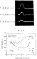
- FIGS. 3(a) - 3(c) show the waveform of current supplied to the bistable magnetic element (amorphous wire) shown in FIG. 2 and the waveforms of the output voltage of the bistable magnetic element, wherein FIG. 3(a) shows the waveform of a pulse current supplied to the amorphous wire shown in FIG. 2, FIG. 3(b) shows the waveform of the output voltage of the amorphous wire shown in FIG. 2 for the storage level 1 , and FIG. 3(c) shows the waveform of the output voltage of the amorphous wire shown in FIG. 2 for the storage level 2 .
- the bistable magnetic element of the present invention can be used as a proximity switch which has high sensitivity and high response speed, and as an NDRO high speed magnetic digital memory element. Since conventional proximity switches for FA are very large (length: about 30 mm, width: about 10 mm, thickness: about 3 mm), they cannot be used in certain technical fields, such as the field of semiconductor manufacturing apparatus, which require small proximity switches.
- the bistable magnetic element of the present invention can be used, as micro proximity switches, in such technical fields.
- FIG. 4 is a graph showing the relationship between an external magnetic field (Oe) applied to a bistable magnetic element (twisted amorphous wire) according to a second embodiment of the present invention and the output voltage (V) of the bistable magnetic element.
- Oe external magnetic field
- V output voltage
- the amorphous wire of the first embodiment shown in FIG. 2 was twisted 20 turns per meter, and the twisted wire was then heated at 500°C for 20 minutes in the air in a furnace.
- the amorphous wire was then quenched in the air outside the furnace. Both ends of the quenched wire having a length of 1 mm were soldered to electrodes, thereby obtaining a sample. This sample was subjected to the same experiment as that in the first embodiment.
- FIGS. 5(a) - 5(c) show the waveform of current supplied to the bistable magnetic element (amorphous wire) shown in FIG. 4 and the waveforms of the output voltage of the bistable magnetic element. That is, FIG. 5(a) shows the waveform of a sharp pulse current (rising time: 3.5 ns, fall time: 3.2 ns, half-value width: 5.8 ns, height: 30 mA) which was supplied to the amorphous wire shown in FIG. 4.
- FIG. 5(b) shows the waveform of the output voltage of the amorphous wire shown in FIG. 4 for the storage level 1
- FIG. 5(c) shows the waveform of the output voltage of the amorphous wire shown in FIG. 4 for the storage level 2 .
- the magnetic field was slightly larger than that in the first embodiment, i.e., about 1.2 Oe.
- the voltage levels for storing the pulse voltage were about 200 mV and about 400 mV.
- the electrodes of the element can be formed easily.
- FIG. 6 is a graph showing the relationship between an external magnetic field (Oe) applied to a bistable magnetic element (amorphous sputtered thin film having no magnetostriction) according to a third embodiment of the present invention and the output voltage (V) of the bistable magnetic element.
- Oe external magnetic field
- V output voltage
- FIG. 6 shows the relationship between the external magnetic field and the output voltage produced between both ends of the wire.
- the amount of jumping and the variation rate are smaller than that those of the amorphous wires of the first and second embodiments.
- An amorphous wire (Co 72.5 Si 12.5 B 15.0 ) of 30 ⁇ m ⁇ (annealed at 475°C for one minute with a tension of 2 kg/mm 2 ) was twisted, and both ends of the wire were soldered to electrodes.
- the wire has a length of 0.5 mm.
- a sharp pulse current (magnitude: 5 mA, frequency: 1 MHz, pulse width: 30 ns) was directly applied to the wire so as to excite it.
- a dc external magnetic field H ex was applied and the pulse-shape output voltage V 0 produced between both ends of the sample was measured.
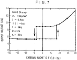
- FIG. 7 is a graph showing the relationship between an external magnetic field (Oe) applied to a bistable magnetic element according to a fourth embodiment of the present invention and the output voltage (mV) of the bistable magnetic element.
- FIG. 7 shows a bistable characteristic for the case where the amount of twist was two turns. The magnitude of the external magnetic field at which the output voltage jumped increased to 8 Oe in the positive range, and to 4 Oe in the negative range.
- the magnitude of the external magnetic field at which the output voltage jumped was about 1 Oe, and the pulse width had to be reduced.
- the effect of the disturbance magnetic fields such as the terrestrial field can be reduced.
- the reason why the bistable characteristics is exhibited is considered that a large Barkhausen effect occurs in the surface portion of the wire.
- the direction of an external magnetic field H ex is close to the direction of the magnetic vector which is inclined at an angle of 45° due to the twist stress, the excitation by the pulse current easily rotates the magnetization vector, so that a high voltage is produced.
- the angle between the external magnetic field Hex and the magnetization vector is equal to or greater than 90° , it becomes difficult to rotate the magnetization vector, so that a low voltage is produced.
- the present invention provides the following effects.
- a micro-sized bistable magnetic element which has high sensitivity and high response speed can be obtained by applying helical magnetic anisotropy to an amorphous wire or the like and by exciting it using a pulse current or a dc-biased high frequency current.
- bistable magnetic element a highly sensitive small-sized proximity switch and an NDRO digital magnetic recording element can be formed. This makes it possible to constitute a magnetic recording apparatus which can perform read/write operation electronically.
Landscapes
- Engineering & Computer Science (AREA)
- Physics & Mathematics (AREA)
- Power Engineering (AREA)
- Computer Hardware Design (AREA)
- Condensed Matter Physics & Semiconductors (AREA)
- General Physics & Mathematics (AREA)
- Electromagnetism (AREA)
- Chemical & Material Sciences (AREA)
- Dispersion Chemistry (AREA)
- Hall/Mr Elements (AREA)
- Soft Magnetic Materials (AREA)
- Measuring Magnetic Variables (AREA)
Applications Claiming Priority (3)
| Application Number | Priority Date | Filing Date | Title |
|---|---|---|---|
| JP23631895A JP3321341B2 (ja) | 1995-09-14 | 1995-09-14 | 双安定磁気素子及びその製造方法 |
| JP236318/95 | 1995-09-14 | ||
| JP23631895 | 1995-09-14 |
Publications (2)
| Publication Number | Publication Date |
|---|---|
| EP0763832A1 true EP0763832A1 (de) | 1997-03-19 |
| EP0763832B1 EP0763832B1 (de) | 2002-06-12 |
Family
ID=16999029
Family Applications (1)
| Application Number | Title | Priority Date | Filing Date |
|---|---|---|---|
| EP96114631A Expired - Lifetime EP0763832B1 (de) | 1995-09-14 | 1996-09-12 | Bistabiles magnetisches Element und Verfahren zu seiner Herstellung |
Country Status (4)
| Country | Link |
|---|---|
| US (1) | US5870328A (de) |
| EP (1) | EP0763832B1 (de) |
| JP (1) | JP3321341B2 (de) |
| DE (1) | DE69621727T2 (de) |
Cited By (5)
| Publication number | Priority date | Publication date | Assignee | Title |
|---|---|---|---|---|
| EP0798751A4 (de) * | 1995-10-13 | 1998-11-18 | Sumitomo Metal Mining Co | Amorphe magnetsubstanz und magnetischer sensor |
| EP0773449A3 (de) * | 1995-11-09 | 1998-11-25 | Research Development Corporation Of Japan | Magnetfeldfühler |
| GB2465369A (en) * | 2008-11-13 | 2010-05-19 | Ingenia Holdings | Magnetic data storage device formed of nanowires with spiral anisotropy in which data is shifted along the wires by application of a rotating magnetic field |
| WO2011009971A1 (es) * | 2009-07-20 | 2011-01-27 | Consejo Superior De Investigaciones Científicas (Csic) | Hilos magnéticos bimetálicos con anisotropía helicoidal, proceso de fabricación y aplicaciones |
| WO2012022300A3 (de) * | 2010-08-14 | 2012-06-14 | Micro-Epsilon Messtechnik Gmbh & Co. Kg | Verfahren und vorrichtung zur erfassung von magnetfeldern |
Families Citing this family (10)
| Publication number | Priority date | Publication date | Assignee | Title |
|---|---|---|---|---|
| SE521232C2 (sv) * | 1997-02-17 | 2003-10-14 | Rso Corp | Givare och metod för beröringsfri detektering av föremål |
| US20030221199A1 (en) * | 1998-10-20 | 2003-11-27 | Whitsett Jeffrey A. | Surfactant protein D for the prevention and diagnosis of pulmonary emphysema |
| DE102005040612A1 (de) * | 2005-08-27 | 2007-03-01 | Behr Gmbh & Co. Kg | Abgaswärmeübertrager |
| DE102005052906A1 (de) * | 2005-11-03 | 2007-05-10 | Heinrich-Heine-Universität Düsseldorf | Sensoranordnung |
| KR100846510B1 (ko) * | 2006-12-22 | 2008-07-17 | 삼성전자주식회사 | 자구벽 이동을 이용한 정보 저장 장치 및 그 제조방법 |
| US7957175B2 (en) | 2006-12-22 | 2011-06-07 | Samsung Electronics Co., Ltd. | Information storage devices using movement of magnetic domain walls and methods of manufacturing the same |
| KR101323716B1 (ko) * | 2007-01-03 | 2013-10-30 | 삼성전자주식회사 | 자구벽 이동을 이용한 정보 저장 장치 및 그 동작방법 |
| CZ2007220A3 (cs) * | 2007-03-23 | 2008-12-17 | Ceské vysoké ucení technické v Praze Fakulta elektrotechnická | Feromagnetická sonda |
| JP5152712B2 (ja) * | 2007-07-17 | 2013-02-27 | 独立行政法人理化学研究所 | 磁化状態制御装置および磁気情報記録装置 |
| ES2581127B2 (es) * | 2016-04-13 | 2017-05-04 | Universidad Complutense De Madrid | Etiqueta, sistema y método para la detección de objetos a larga distancia |
Citations (1)
| Publication number | Priority date | Publication date | Assignee | Title |
|---|---|---|---|---|
| EP0448114A1 (de) * | 1990-03-23 | 1991-09-25 | Unitika Ltd. | Dünnfilm magnetisches Material und Verfahren zur Herstellung |
Family Cites Families (7)
| Publication number | Priority date | Publication date | Assignee | Title |
|---|---|---|---|---|
| US3173131A (en) * | 1958-03-19 | 1965-03-09 | Bell Telephone Labor Inc | Magneostrictive apparatus |
| US3320596A (en) * | 1961-12-07 | 1967-05-16 | Shell Oil Co | Storing and recalling signals |
| US3902167A (en) * | 1974-02-25 | 1975-08-26 | Honeywell Inc | Magnetic thin film switch |
| US4236230A (en) * | 1977-12-19 | 1980-11-25 | International Business Machines Corporation | Bistable magnetostrictive device |
| US4451876A (en) * | 1981-06-19 | 1984-05-29 | Hitachi Metals, Ltd. | Switching regulator |
| US4913750A (en) * | 1987-03-06 | 1990-04-03 | Jeco Company Limited | Amorphous magnetic wire |
| DE3843087C2 (de) * | 1987-12-21 | 2001-09-13 | Tdk Corp | Magnetfeldsensor |
-
1995
- 1995-09-14 JP JP23631895A patent/JP3321341B2/ja not_active Expired - Fee Related
-
1996
- 1996-09-09 US US08/709,907 patent/US5870328A/en not_active Expired - Fee Related
- 1996-09-12 DE DE69621727T patent/DE69621727T2/de not_active Expired - Lifetime
- 1996-09-12 EP EP96114631A patent/EP0763832B1/de not_active Expired - Lifetime
Patent Citations (1)
| Publication number | Priority date | Publication date | Assignee | Title |
|---|---|---|---|---|
| EP0448114A1 (de) * | 1990-03-23 | 1991-09-25 | Unitika Ltd. | Dünnfilm magnetisches Material und Verfahren zur Herstellung |
Non-Patent Citations (5)
| Title |
|---|
| KITO T ET AL: "ASYMMETRICAL MAGNETO-IMPEDANCE IN TWISTED AMORPHOUS WIRES MAGNETIZED WITH ASYMMETRICAL CURRENT FOR LINEAR FIELD SENSORS", 18 April 1995, 1995 DIGESTS OF INTERMAG. INTERNATIONAL MAGNETICS CONFERENCE, SAN ANTONIO, APR. 18 - 21, 1995, PAGE(S) AS-03, INSTITUTE OF ELECTRICAL AND ELECTRONICS ENGINEERS, XP000581847 * |
| MIZUTANI M ET AL: "DISTANCE SENSORS USING DOMAIN WALL PROPAGATION DRIVEN BY A WIRE CURRENT PULSE TRAIN AMORPHOUS MAGNETOSTRICTIVE WIRES", IEEE TRANSLATION JOURNAL ON MAGNETICS IN JAPAN, vol. 9, no. 6, 1 November 1994 (1994-11-01), pages 15 - 20, XP000548720 * |
| Y.SHIMADA ET AL: "Sputtering of FeCoB Amorphous Films with Soft Magnetic Properties", IEEE TRANSACTIONS ON MAGNETICS, vol. 17, no. 2, March 1981 (1981-03-01), NEW YORK US, pages 1199 - 1203, XP002023757 * |
| YAMASAKI J ET AL: "HELICAL ANISOTROPY AND MATTEUCCI EFFECT IN CO-SI-B AMORPHOUS WIRES WITH NEGATIVE MAGNETOSTRICTION", JOURNAL OF APPLIED PHYSICS, vol. 75, no. 10, PART 02B, 15 May 1994 (1994-05-15), pages 6958, XP000458270 * |
| YAMASAKI J: "SENSING FUNCTION IN AMORPHOUS MAGNETIC MATERIALS", IEEE TRANSLATION JOURNAL ON MAGNETICS IN JAPAN, vol. 7, no. 9, 1 September 1992 (1992-09-01), pages 694 - 704, XP000348905 * |
Cited By (10)
| Publication number | Priority date | Publication date | Assignee | Title |
|---|---|---|---|---|
| EP0798751A4 (de) * | 1995-10-13 | 1998-11-18 | Sumitomo Metal Mining Co | Amorphe magnetsubstanz und magnetischer sensor |
| EP0773449A3 (de) * | 1995-11-09 | 1998-11-25 | Research Development Corporation Of Japan | Magnetfeldfühler |
| GB2465369A (en) * | 2008-11-13 | 2010-05-19 | Ingenia Holdings | Magnetic data storage device formed of nanowires with spiral anisotropy in which data is shifted along the wires by application of a rotating magnetic field |
| GB2465369B (en) * | 2008-11-13 | 2011-01-12 | Ingenia Holdings | Magnetic data storage device and method |
| WO2011009971A1 (es) * | 2009-07-20 | 2011-01-27 | Consejo Superior De Investigaciones Científicas (Csic) | Hilos magnéticos bimetálicos con anisotropía helicoidal, proceso de fabricación y aplicaciones |
| ES2352631A1 (es) * | 2009-07-20 | 2011-02-22 | Consejo Superior De Investigaciones Cientificas (Csic) | Hilos magneticos bimetalicos con anisotropia helicoidal, proceso de fabricacion y aplicaciones. |
| WO2012022300A3 (de) * | 2010-08-14 | 2012-06-14 | Micro-Epsilon Messtechnik Gmbh & Co. Kg | Verfahren und vorrichtung zur erfassung von magnetfeldern |
| CN103140741A (zh) * | 2010-08-14 | 2013-06-05 | 微-埃普西龙测量技术有限两合公司 | 用于检测磁场的方法和设备 |
| CN103140741B (zh) * | 2010-08-14 | 2016-04-27 | 微-埃普西龙测量技术有限两合公司 | 用于检测磁场的方法和设备 |
| US9574865B2 (en) | 2010-08-14 | 2017-02-21 | Micro-Epsilon Messtechnik Gmbh & Co. Kg | Method and apparatus for sensing magnetic fields |
Also Published As
| Publication number | Publication date |
|---|---|
| DE69621727D1 (de) | 2002-07-18 |
| JPH0982082A (ja) | 1997-03-28 |
| JP3321341B2 (ja) | 2002-09-03 |
| EP0763832B1 (de) | 2002-06-12 |
| DE69621727T2 (de) | 2003-01-30 |
| US5870328A (en) | 1999-02-09 |
Similar Documents
| Publication | Publication Date | Title |
|---|---|---|
| EP0763832B1 (de) | Bistabiles magnetisches Element und Verfahren zu seiner Herstellung | |
| US6809515B1 (en) | Passive solid-state magnetic field sensors and applications therefor | |
| Hristoforou et al. | Magnetostriction and magnetostrictive materials for sensing applications | |
| US6809516B1 (en) | Passive magnetic field sensors having magnetostrictive and piezoelectric materials | |
| US4247601A (en) | Switchable magnetic device | |
| KR101030110B1 (ko) | 박막형 3축 플럭스게이트 및 그 제조방법 | |
| Vazquez et al. | Magnetic bistability of amorphous wires and sensor applications | |
| US5994899A (en) | Asymmetrical magneto-impedance element having a thin magnetic wire with a spiral magnetic anisotropy | |
| JPS61260321A (ja) | 位置検出装置 | |
| JP6514515B2 (ja) | 起電力発生装置 | |
| US4591788A (en) | Magnetic field sensing device | |
| Mohri et al. | Sensitive bistable magnetic sensors using twisted amorphous magnetostrictive ribbons due to Matteucci effect | |
| EP0321791A2 (de) | Magnetischer Dehnungsmessstreifen | |
| CN105355778B (zh) | 磁电隔离器、磁存储器、磁电流传感器和磁温度传感器 | |
| JPH11109006A (ja) | 磁気インピーダンスセンサ | |
| Datta et al. | Saturation and engineering magnetostriction of an iron‐base amorphous alloy for power applications | |
| Wun-Fogle et al. | Enhancement of magnetostrictive effects for sensor applications | |
| Pohm et al. | Magnetic film memories, a survey | |
| Yamasaki | Sensing function in amorphous magnetic materials | |
| Garcı́a-Miquel et al. | Domain wall propagation in bistable amorphous wires | |
| Abe et al. | Annealing and torsion stress effect on magnetic anisotropy and magnetostriction of Vicalloy fine wire | |
| US3735369A (en) | Magnetic memory employing force detecting element | |
| US2711509A (en) | Testing of magnetic materials | |
| Abe et al. | Dependence of large Barkhausen jump on length of a vicalloy fine wire with torsion stress | |
| Abe et al. | Induced pulse voltage in twisted Vicalloy wire with compound magnetic effect |
Legal Events
| Date | Code | Title | Description |
|---|---|---|---|
| PUAI | Public reference made under article 153(3) epc to a published international application that has entered the european phase |
Free format text: ORIGINAL CODE: 0009012 |
|
| AK | Designated contracting states |
Kind code of ref document: A1 Designated state(s): DE FR GB |
|
| 17P | Request for examination filed |
Effective date: 19970828 |
|
| 17Q | First examination report despatched |
Effective date: 19990525 |
|
| GRAG | Despatch of communication of intention to grant |
Free format text: ORIGINAL CODE: EPIDOS AGRA |
|
| GRAG | Despatch of communication of intention to grant |
Free format text: ORIGINAL CODE: EPIDOS AGRA |
|
| GRAH | Despatch of communication of intention to grant a patent |
Free format text: ORIGINAL CODE: EPIDOS IGRA |
|
| GRAH | Despatch of communication of intention to grant a patent |
Free format text: ORIGINAL CODE: EPIDOS IGRA |
|
| GRAA | (expected) grant |
Free format text: ORIGINAL CODE: 0009210 |
|
| AK | Designated contracting states |
Kind code of ref document: B1 Designated state(s): DE FR GB |
|
| REG | Reference to a national code |
Ref country code: GB Ref legal event code: FG4D |
|
| REF | Corresponds to: |
Ref document number: 69621727 Country of ref document: DE Date of ref document: 20020718 |
|
| ET | Fr: translation filed | ||
| PLBE | No opposition filed within time limit |
Free format text: ORIGINAL CODE: 0009261 |
|
| STAA | Information on the status of an ep patent application or granted ep patent |
Free format text: STATUS: NO OPPOSITION FILED WITHIN TIME LIMIT |
|
| 26N | No opposition filed |
Effective date: 20030313 |
|
| PGFP | Annual fee paid to national office [announced via postgrant information from national office to epo] |
Ref country code: FR Payment date: 20060821 Year of fee payment: 11 |
|
| PGFP | Annual fee paid to national office [announced via postgrant information from national office to epo] |
Ref country code: GB Payment date: 20060906 Year of fee payment: 11 |
|
| PGFP | Annual fee paid to national office [announced via postgrant information from national office to epo] |
Ref country code: DE Payment date: 20060929 Year of fee payment: 11 |
|
| PG25 | Lapsed in a contracting state [announced via postgrant information from national office to epo] |
Ref country code: DE Free format text: LAPSE BECAUSE OF THE APPLICANT RENOUNCES Effective date: 20070711 |
|
| GBPC | Gb: european patent ceased through non-payment of renewal fee |
Effective date: 20070912 |
|
| REG | Reference to a national code |
Ref country code: FR Ref legal event code: ST Effective date: 20080531 |
|
| PG25 | Lapsed in a contracting state [announced via postgrant information from national office to epo] |
Ref country code: FR Free format text: LAPSE BECAUSE OF NON-PAYMENT OF DUE FEES Effective date: 20071001 |
|
| PG25 | Lapsed in a contracting state [announced via postgrant information from national office to epo] |
Ref country code: GB Free format text: LAPSE BECAUSE OF NON-PAYMENT OF DUE FEES Effective date: 20070912 |