EP0764868A1 - Verfahren zur Korrektur von Bildfeldwölbung und dessen Anwendung in einer optischen Strahlabtastvorrichtung - Google Patents
Verfahren zur Korrektur von Bildfeldwölbung und dessen Anwendung in einer optischen Strahlabtastvorrichtung Download PDFInfo
- Publication number
- EP0764868A1 EP0764868A1 EP96115155A EP96115155A EP0764868A1 EP 0764868 A1 EP0764868 A1 EP 0764868A1 EP 96115155 A EP96115155 A EP 96115155A EP 96115155 A EP96115155 A EP 96115155A EP 0764868 A1 EP0764868 A1 EP 0764868A1
- Authority
- EP
- European Patent Office
- Prior art keywords
- optical beam
- lens
- scanning
- optical
- image surface
- Prior art date
- Legal status (The legal status is an assumption and is not a legal conclusion. Google has not performed a legal analysis and makes no representation as to the accuracy of the status listed.)
- Withdrawn
Links
- 230000003287 optical effect Effects 0.000 title claims abstract description 180
- 238000000034 method Methods 0.000 title claims abstract description 20
- 239000004065 semiconductor Substances 0.000 claims description 31
- 238000003384 imaging method Methods 0.000 claims description 19
- 230000008859 change Effects 0.000 claims description 11
- 238000006073 displacement reaction Methods 0.000 description 4
- XKRFYHLGVUSROY-UHFFFAOYSA-N Argon Chemical compound [Ar] XKRFYHLGVUSROY-UHFFFAOYSA-N 0.000 description 2
- 230000002411 adverse Effects 0.000 description 2
- 229910052786 argon Inorganic materials 0.000 description 1
- 230000006866 deterioration Effects 0.000 description 1
- CPBQJMYROZQQJC-UHFFFAOYSA-N helium neon Chemical compound [He].[Ne] CPBQJMYROZQQJC-UHFFFAOYSA-N 0.000 description 1
- 239000000463 material Substances 0.000 description 1
- 230000007246 mechanism Effects 0.000 description 1
- 238000012986 modification Methods 0.000 description 1
- 230000004048 modification Effects 0.000 description 1
- 230000004044 response Effects 0.000 description 1
- 230000001629 suppression Effects 0.000 description 1
- 238000011144 upstream manufacturing Methods 0.000 description 1
Images





Classifications
-
- G—PHYSICS
- G02—OPTICS
- G02B—OPTICAL ELEMENTS, SYSTEMS OR APPARATUS
- G02B26/00—Optical devices or arrangements for the control of light using movable or deformable optical elements
- G02B26/08—Optical devices or arrangements for the control of light using movable or deformable optical elements for controlling the direction of light
- G02B26/10—Scanning systems
- G02B26/12—Scanning systems using multifaceted mirrors
- G02B26/124—Details of the optical system between the light source and the polygonal mirror
Definitions
- the present invention relates to a method of correcting curvature of image surface which is created in an optical beam scanning apparatus in which an optical beam from a light source impinges upon a deflecting system and a surface-to-be-scanned is scanned through a scanning lens with the light beam which is deflected by the deflecting system in a main scanning direction, and also relates to an optical beam scanning apparatus for such a method.
- curvature of image surface refers to curvature of image surface in a main scanning direction.
- Fig. 13 is a plan view showing a conventional optical beam scanning apparatus.
- this optical beam scanning apparatus comprises a first optical part 10 which is formed by a semiconductor laser 11 and a collimator lens 12. An optical beam emitted from the semiconductor laser 11 is shaped by the collimator lens 12, and then emitted toward a galvanometer 30 which rotates about an axis 31.
- a scanning lens 40 is disposed between the galvanometer 30 and a surface-to-be-scanned S so that an optical beam deflected by the galvanometer 30 is focused on the surface-to-be-scanned S.
- the optical beam scanning apparatus shown in Fig. 13 is a pre-objective type optical beam scanning apparatus in which the galvanometer 30 is disposed on an upstream side to the scanning lens 40, i.e., on the first optical part 10 side.
- An optical beam from the first optical part 10 is deflected by the galvanometer 30, and a deflected light beam scans the surface-to-be-scanned S through the scanning lens 40 in the main scanning direction Y.
- a beam diameter within an optical beam scanning apparatus is relatively large and a depth of focus d is relatively deep as shown in Fig. 13. Therefore, it is possible to position an image surface I within the depth of focus d over the entire scanning range and hence to draw excellently, even if the curvature of image surface in the main scanning direction Y is somewhat large.
- curvature of image surface is suppressed by designing the scanning lens 40 so that curvature of image surface is reduced as much as possible, it is not possible to suppress curvature of image surface only by means of optimum designing. This is because curvature of image surface is susceptible to the surface accuracy of a lens, so that a deterioration in the surface accuracy of the lens during processing of the lens remarkably increases curvature of image surface and therefore the problem above is created. On the other hand, if the surface accuracy of the lens during processing of the lens is increased for the purpose of suppressing curvature of image surface, another problem of an increased cost is created.
- the image surface I may be adjusted so as to be positioned within the depth of focus over the entire scanning range by moving the imaging position in an optical axis direction Z.
- the depth of focus is relatively shallow as compared with the curvature of image surface as shown in Fig. 13, it is impossible to position the entire image surface I within the depth of focus even though the imaging position is simply moved.
- the present invention is directed to a curvature of image surface correction method for correcting curvature of image surface which is created in an optical beam scanning apparatus in which an optical beam from a light source impinges upon a deflecting system and a deflected optical beam from the deflecting system scans a surface-to-be-scanned through a scanning lens in a main scanning direction, comprising the steps of: (a) scanning the surface-to-be-scanned with the optical beam; (b) judging whether an image surface which is created by the optical beam scanning apparatus is positioned within the depth of focus of the optical beam scanning apparatus over an entire scanning range; and (c) changing the degree of parallel of the optical beam which is incident upon the deflecting system and adjusting the shape of the image surface when the image surface is not positioned within the depth of focus of the optical beam scanning apparatus over the entire scanning range, to thereby position the image surface within the depth of focus of the optical beam scanning apparatus over the entire scanning range.
- a first object of the present invention is to provide for a curvature of image surface correction method with which curvature of image surface is reduced without improving the surface accuracy of a lens.
- a second object of the present invention is to provide for an optical beam scanning apparatus for use with the curvature of image surface correction method above, with which by reducing curvature of image surface it is possible to draw at an excellent image quality over an entire scanning range.
- the method further comprises the step of: (d) moving optical elements starting from the light source to the scanning lens as one unit along an optical axis of the optical beam scanning apparatus after adjusting the shape of the image surface, to thereby approximately coincide an imaging position of the optical beam scanning apparatus with the surface-to-be-scanned.
- the deflecting system includes a polygon mirror
- the optical beam scanning apparatus includes a plurality of inclination compensation lenses for compensating inclination of reflecting surfaces of the polygon mirror
- the method further comprises the step of: (e) moving each one of the plurality of inclination compensation lenses to thereby compensate inclination of the reflecting surfaces of the polygon mirror.
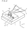
- Fig. 1 is a perspective view of an optical beam scanning apparatus according to a first preferred embodiment of the present invention.
- a guide 2 is fixedly adhered on an optical base 1, and another optical base 3 is disposed along the guide 2 for free reciprocal movement.
- a semiconductor laser 11 is held by a laser holder 13, and a collimator lens 12 is held by a lens holder 14.
- the semiconductor laser 11 is directly modulated and drived based on a signal which is received from a control part (not shown) which controls the entire apparatus, so that on a surface-to-be-scanned S, an optical beam is emitted from the semiconductor laser 11 over a pixel which is to be recorded so as to irradiate and expose the surface-to-be-scanned S, and emission of an optical beam from the semiconductor laser 11 is stopped over a pixel which is not to be recorded.
- An optical beam which is emitted from the semiconductor laser 11 in this manner is shaped by the collimator lens 12 and discharged toward a galvanometer 30.
- the optical beam from the semiconductor laser 11 is shaped by the collimator lens 12 into a parallel optical beam and discharged toward the galvanometer 30.
- a first optical part 10 is formed by the semiconductor laser 11 and the collimator lens 12 in this preferred embodiment
- the structure of the first optical part 10 is not limited to this, but may be formed by a light source such as a helium-neon laser and an argon laser which cannot be directly modulated and a modulator which modulates an optical beam from the light source, for instance.
- an LED Light Emitting Diode
- the laser holder 13 is fixedly adhered to the optical base 3, while the semiconductor laser 11 is fixed to the optical base 3.
- the lens holder 14 is freely movable on the optical base 3 along a guide 15.
- an operator manipulates an adjustment screw 16
- the lens holder 14 moves, thereby moving and positioning the collimator lens 12 along an optical axis OA.
- adjusting means for changing the degree of parallel of an optical beam which is to be incident upon the galvanometer (i.e., deflecting system) 30 is formed by the lens holder 14, the guide 15, and the adjustment screw 16, and the shape of the image surface is changed when the degree of parallel of an optical beam which is incident upon the galvanometer 30 is changed by the adjusting means.
- deflecting system i.e., deflecting system
- the galvanometer 30 is disposed on the optical base 3, for free rotation about an axis 31, so as to deflect an optical beam from the first optical part 10 and guide the same toward the scanning lens 40 side.
- the deflecting system for deflecting an optical beam is not limited to the galvanometer 30, but may be a resonant scanner (resonance type galvanometer), a penta-prism, a monogon mirror, a polygon mirror, etc.
- a polygon mirror is used as the deflecting system, it is essential to compensate inclination of reflecting surfaces of the polygon mirror. As this is a little different from this preferred embodiment, this will be described in detail later as another preferred embodiment.
- the scanning lens 40 is fixedly adhered to the optical base 3 while held by a lens holder 41, so as to guide an optical beam from the galvanometer 30 toward the surface-to-be-scanned S.
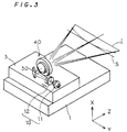
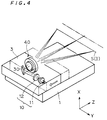
- an adjustment knob 4 is linked to the optical base 3 seating the semiconductor laser 11, the collimator lens 12, the adjusting means, the galvanometer 30, and the scanning lens 40. Therefore, the optical base 3 is moved along the guide 2 when an operator manipulates the adjustment knob 4, so that the optical elements starting from the first optical part 10 to the scanning lens 40 (i.e., the semiconductor laser 11, the collimator lens 12, the adjusting means, the galvanometer 30, and the scanning lens 40) are moved and positioned as one unit.
- the imaging position of an image surface which is formed by the optical beam scanning apparatus is moved in the optical axis direction Z.
- imaging position changing means functioning as such is formed by the guide 2 and the adjustment knob 4.
- the imaging position i.e., the position of the image surface I
- the adjustment knob 4 is operated to move the optical base 3 in the direction of the white arrow and move the optical elements mounted on the optical base 3 (i.e., the semiconductor laser 11, the collimator lens 12, the galvanometer 30, and the scanning lens 40) as one unit in a direction (-Z), so that the image surface I is coincided with the surface-to-be-scanned S. Since this positions the entire image surface within the depth of focus over the entire scanning range without fail, drawing is performed with an excellent image quality.
- the optical beam scanning apparatus can reduce curvature of image surface and perform drawing with an excellent image quality over the entire scanning range while preventing an increase in a cost of the apparatus.
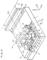
- Fig. 5 is a perspective view of an optical beam scanning apparatus according to a second preferred embodiment of the present invention. This optical beam scanning apparatus is largely different from that of the first preferred embodiment described above with respect to the following three points.
- a first difference is use of a polygon mirror 32 as the deflecting system.
- a second difference is disposition of cylindrical lenses 20, 50 each having a power only in a sub scanning direction X for the purpose of compensating inclination of reflecting surfaces of the polygon mirror which is associated with use of the polygon mirror 32.
- the cylindrical lens 20 is disposed between a mirror 17, which guides an optical beam from the collimator lens 12 toward the polygon mirror 32 side, and the polygon mirror 32.
- the cylindrical lens 50 is disposed between the scanning lens 40 and the surface-to-be-scanned S.
- the cylindrical lenses 20 and 50 are held by lens holder 21 and 51, respectively, and are freely movable along the optical axis OA on optical bases 3 and 1, respectively.
- the lens holder 21 is movable along a guide 22 which is fixedly adhered to the optical base 3, so that by moving the lens holder 21 by means of an adjustment screw 23, the cylindrical lens 20 is positioned.
- curvature of image surface may be created as in the first preferred embodiment.
- the image surface is carved toward an over side.
- the cylindrical lens (i.e., first inclination compensation lens) 20 is moved toward the collimator lens 12 side as indicated by the arrow R 2 in Fig. 6, so that the semiconductor laser 11 and the mirror surface 33 of the polygon mirror 32 are adjusted so as to be optically conjugate with each other in the sub scanning direction X.
- the lens holder 21 since an operator moves the lens holder 21 along the guide 22 by means of the adjustment screw 23, the lens holder 21, the guide 22 and the adjustment screw 23 serve as first moving means for inclination compensation which make the semiconductor laser 11 and the mirror surface 33 of the polygon mirror 32 optically conjugate with each other in the sub scanning direction X.
- cylindrical lens (i.e., first inclination compensation lens) 20 is moved after the shape of the image surface is adjusted by moving the collimator lens 12 in this preferred embodiment, such adjustment may be achieved by performing these operations in a reverse order or by moving the lenses 12 and 20 alternately.
- the imaging position i.e., the position of the image surface I
- the adjustment knob 4 is operated to move the optical base 3 in the direction of the arrow R 3 and move the optical elements which are mounted on the optical base 3 (i.e., the elements enclosed in the dotted line in Fig. 7: the semiconductor laser 11, the collimator lens 12, the mirror 17, the cylindrical lens 20, the polygon mirror 32 and the scanning lens 40) as one unit, so that the image surface I is coincided with the surface-to-be-scanned S. Since this position the entire image surface within the depth of focus over the entire scanning range without fail, drawing is performed with an excellent image quality.
- the mirror surface 33 of the polygon mirror 32 and the surface-to-be-scanned S are not optically conjugate with each other any more in the sub scanning direction X as the scanning lens 40 is moved, in many cases, since the quantity of displacement from the conjugate relationship is relatively small (this is because displacement is approximately within the range of the depth of focus), there is almost no influence due to inclination of reflecting surfaces of the polygon mirror 32.
- the cylindrical lens 50 is moved toward the surface-to-be-scanned S side as indicated by the arrow R 4 in Fig. 8 and accordingly adjusting the mirror surface 33 of the polygon mirror 32 and the surface-to-be-scanned S so as to be completely optically conjugate with each other in the sub scanning direction X.
- two long holes 52 are formed in a lower portion of the lens holder 51. After moving and positioning the cylindrical lens 50 within the range between the long holes 52, the lens holder 51 is fixed to the optical base 1 by means of a bolt (not shown). This structure corresponds to second moving means for inclination compensation of inclination of reflecting surfaces of the polygon mirror.
- the optical beam scanning apparatus can reduce curvature of image surface and perform drawing with an excellent image quality over the entire scanning range while preventing an increase in a cost of the appratus.
- cylindrical lenses 20, 50 for compensation of inclination of reflecting surfaces of the polygon mirror are freely movable in the optical axis direction Z, and inclination of reflecting surfaces of the polygon mirror is compensated moving the cylindrical lens 20 in accordance with movement of the collimator lens 12 and/or the cylindrical lens 50 in accordance with movement of the optical base 3, it is possible to perform excellent drawing while suppressing an influence of inclination of reflecting surfaces of the polygon mirror.
- the imaging position changing means for moving the optical base 3, the adjusting means for moving the collimator lens 12, the first moving means for compensating inclination of reflecting surfaces of the polygon mirror which moves the cylindrical lens 20, and the second moving means for compensating inclination of reflecting surfaces of the polygon mirror which moves the cylindrical lens 50 are not limited to the structures described above. Rather, a motor driving mechanism may be mounted instead of the adjustment knob 4 to automatically adjust in response to a signal from the control part.
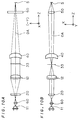
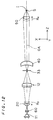
- Fig. 9 is a perspective view of an optical beam scanning apparatus according to a third preferred embodiment of the present invention.
- Figs. 10A and 10B are plan views of the optical beam scanning apparatus of Fig. 9.
- Fig. 10A is a plan view taken at a main scanning surface (i.e., YZ plane), while Fig. 10B is a plan view taken at a sub scanning surface (i.e., XZ plane).
- this optical beam scanning apparatus is different from that of the third preferred embodiment with respect to the following points.
- the semiconductor laser 11 and a relay lens 60 are held by the lens holder 13, so that an intermediate image of the semiconductor laser 11 is formed at an emission side of the relay lens 60.
- a positional relationship between the cylindrical lens 20 and the collimator lens 12 is reverse. That is, in the optical beam scanning apparatus according to this preferred embodiment, as shown in Figs. 9, 10A and 10B, an optical beam from the semiconductor laser 11 is incident upon the cylindrical lens 20, which has a power only in the sub scanning direction X, through the relay lens 60, shaped by the collimator lens 12, and thereafter guided into the polygon mirror 32 through the mirror 17.
- the optical beam scanning apparatus shown in Fig. 5 requires all optical elements from the semiconductor laser 11 to the scanning lens 40 to be mounted on the optical base 3 so that these optical elements are freely movable in the optical axis direction Z as one unit
- the optical beam scanning apparatus according to this preferred embodiment only the mirror 17, the polygon mirror 32 and the scanning lens 40 are fixed on the optical base 3 so that only the mirror 17, the polygon mirror 32 and the scanning lens 40 are freely moved in the optical axis direction Z as the adjustment knob 4 is manipulated.
- curvature of image surface may be created as in the preferred embodiments describe earlier. In this preferred embodiment as well, for convenience of description, it is assumed here that the image surface is carved toward an over side.
- the imaging position i.e., the position of the image surface I
- the adjustment knob 4 is operated to move the mirror 17, the polygon mirror 32 and the scanning lens 40 as one unit together with the optical base 3, thereby moving the scanning lens 40 away from the surface-to-be-scanned S as indicated by the arrow R 22 in Fig. 11.
- the mirror surface 33 of the polygon mirror 32 is moved away from the collimator lens 12 as indicated by the arrow R 21 in Fig. 11. While Fig.
- FIG. 11 shows the mirror surface 33 of the polygon mirror 32 and the scanning lens 40 as they come close to each other as the optical base 3 is moved in this manner, this is to clearly illustrate a manner in which the mirror surface 33 and the scanning lens 40 are moved away from the collimator lens 12 and the surface-to-be-scanned S, respectively.
- a distance between the both optical elements (i.e., the polygon mirror 32 and the scanning lens 40) which are fixed to the optical base 3 is always constant, as can be understood from Fig. 9.
- the mirror surface 33 of the polygon mirror 32 and the surface-to-be-scanned S are not optically conjugate with each other any more in the sub scanning direction X as the polygon mirror 32 and the scanning lens 40 are moved, in many cases, since the quantity of displacement from the conjugate relationship is relatively small (this is because displacement is approximately within the range of the depth of focus), there is almost no influence due to inclination of reflecting surfaces of the polygon mirror 32.
- the optical beam scanning apparatus can reduce curvature of image surface and perform drawing with an excellent image quality over the entire scanning range while preventing an increase in a cost of the appratus.
- cylindrical lenses 20, 50 for compensating inclination of reflecting surfaces of the polygon mirror are freely movable in the optical axis direction Z and inclination of reflecting surfaces of the polygon mirror is compensated by moving the cylindrical lenses 20, 50 if necessary, it is possible to perform excellent drawing while compensating inclination of reflecting surfaces of the polygon mirror.
- the adjusting means moves the collimator lens 12 so that the degree of parallel of an optical beam which is incident upon the deflecting system is changed and the shape of the image surface is adjusted
- the collimator lens 12 may be fixed while only the semiconductor laser 11 may be moved, or both the semiconductor laser 11 and the collimator lens 12 may be moved.
- a cylindrical lens having a power in the main scanning direction Y may be disposed between the first optical part 10 and the deflecting system, and the adjusting means may be structured so as to move this cylindrical lens along the optical axis OA.
- Such adjusting means as well can change the degree of parallel of an optical beam which impinges upon the deflecting system and adjust the shape of the image surface, like the adjusting means described above.
Landscapes
- Physics & Mathematics (AREA)
- General Physics & Mathematics (AREA)
- Optics & Photonics (AREA)
- Mechanical Optical Scanning Systems (AREA)
Applications Claiming Priority (4)
| Application Number | Priority Date | Filing Date | Title |
|---|---|---|---|
| JP244435/95 | 1995-09-22 | ||
| JP24443595 | 1995-09-22 | ||
| JP28350695A JP3545115B2 (ja) | 1995-09-22 | 1995-10-31 | 像面湾曲の補正方法および該方法に使用する光ビーム走査装置 |
| JP283506/95 | 1995-10-31 |
Publications (1)
| Publication Number | Publication Date |
|---|---|
| EP0764868A1 true EP0764868A1 (de) | 1997-03-26 |
Family
ID=26536740
Family Applications (1)
| Application Number | Title | Priority Date | Filing Date |
|---|---|---|---|
| EP96115155A Withdrawn EP0764868A1 (de) | 1995-09-22 | 1996-09-20 | Verfahren zur Korrektur von Bildfeldwölbung und dessen Anwendung in einer optischen Strahlabtastvorrichtung |
Country Status (3)
| Country | Link |
|---|---|
| US (1) | US5808774A (de) |
| EP (1) | EP0764868A1 (de) |
| JP (1) | JP3545115B2 (de) |
Cited By (1)
| Publication number | Priority date | Publication date | Assignee | Title |
|---|---|---|---|---|
| EP1014149A1 (de) * | 1998-12-21 | 2000-06-28 | Xerox Corporation | Rasterabtastvorrichtung |
Families Citing this family (12)
| Publication number | Priority date | Publication date | Assignee | Title |
|---|---|---|---|---|
| JP3679560B2 (ja) * | 1997-08-22 | 2005-08-03 | キヤノン株式会社 | 走査光学系の調整方法 |
| JPH11305152A (ja) * | 1998-04-21 | 1999-11-05 | Asahi Optical Co Ltd | 走査光学装置 |
| JP2000105347A (ja) * | 1998-07-29 | 2000-04-11 | Ricoh Co Ltd | マルチビ―ム光源装置、マルチビ―ム走査装置および画像形成装置 |
| JP4007705B2 (ja) | 1998-11-20 | 2007-11-14 | 富士通株式会社 | 光走査型タッチパネル |
| US6657760B2 (en) * | 2000-01-14 | 2003-12-02 | Canon Kabushiki Kaisha | Image scanning apparatus |
| US7158321B2 (en) * | 2004-03-19 | 2007-01-02 | Lexmark International, Inc. | Pre-scan assembly for aligning a pre-scan lens in a laser scanning unit |
| JP5112098B2 (ja) * | 2008-02-05 | 2013-01-09 | 株式会社リコー | 光走査装置及び画像形成装置 |
| JP2010002852A (ja) * | 2008-06-23 | 2010-01-07 | Ricoh Co Ltd | 光走査光学系、光走査装置並びにそれを用いた画像形成装置 |
| JP6016645B2 (ja) * | 2013-01-09 | 2016-10-26 | シャープ株式会社 | 光走査装置、及びそれを備えた画像形成装置 |
| CN104536132A (zh) * | 2014-12-09 | 2015-04-22 | 中国科学院上海技术物理研究所 | 一种多孔径近距大视区光学系统及扫描镜的设计方法 |
| JP6504450B2 (ja) * | 2015-06-16 | 2019-04-24 | 株式会社リコー | 光源装置及びこの光源装置を用いた光走査装置、物体検出装置 |
| GB2566695A (en) * | 2017-09-20 | 2019-03-27 | Stratec Biomedical Ag | Scanning device and method for use in an automated analyzer |
Citations (5)
| Publication number | Priority date | Publication date | Assignee | Title |
|---|---|---|---|---|
| JPS58190920A (ja) * | 1982-05-01 | 1983-11-08 | Ricoh Co Ltd | 光走査装置 |
| JPS63216018A (ja) * | 1987-03-05 | 1988-09-08 | Sankyo Seiki Mfg Co Ltd | 光走査装置 |
| US4941719A (en) * | 1986-05-23 | 1990-07-17 | Hitachi, Ltd. | Light scanning system |
| EP0465136A2 (de) * | 1990-06-27 | 1992-01-08 | Xerox Corporation | Optischer Abtastapparat mit submikoner Schwankungskorrektur |
| EP0599542A1 (de) * | 1992-11-27 | 1994-06-01 | Xerox Corporation | Optisches System aus zwei Elementen zur Kompensation des Brennpunktsfehlers in Laserabtastsystemen |
Family Cites Families (3)
| Publication number | Priority date | Publication date | Assignee | Title |
|---|---|---|---|---|
| JPS58192015A (ja) * | 1982-05-04 | 1983-11-09 | Toshiba Corp | 複数光束走査装置 |
| US5054866A (en) * | 1988-12-29 | 1991-10-08 | Ricoh Company, Ltd. | Scanning optical apparatus |
| US5134511A (en) * | 1989-12-08 | 1992-07-28 | Kabushiki Kaisha Toshiba | Optical unit for use in laser beam printer or the like |
-
1995
- 1995-10-31 JP JP28350695A patent/JP3545115B2/ja not_active Expired - Lifetime
-
1996
- 1996-09-19 US US08/715,547 patent/US5808774A/en not_active Expired - Lifetime
- 1996-09-20 EP EP96115155A patent/EP0764868A1/de not_active Withdrawn
Patent Citations (5)
| Publication number | Priority date | Publication date | Assignee | Title |
|---|---|---|---|---|
| JPS58190920A (ja) * | 1982-05-01 | 1983-11-08 | Ricoh Co Ltd | 光走査装置 |
| US4941719A (en) * | 1986-05-23 | 1990-07-17 | Hitachi, Ltd. | Light scanning system |
| JPS63216018A (ja) * | 1987-03-05 | 1988-09-08 | Sankyo Seiki Mfg Co Ltd | 光走査装置 |
| EP0465136A2 (de) * | 1990-06-27 | 1992-01-08 | Xerox Corporation | Optischer Abtastapparat mit submikoner Schwankungskorrektur |
| EP0599542A1 (de) * | 1992-11-27 | 1994-06-01 | Xerox Corporation | Optisches System aus zwei Elementen zur Kompensation des Brennpunktsfehlers in Laserabtastsystemen |
Non-Patent Citations (2)
| Title |
|---|
| PATENT ABSTRACTS OF JAPAN vol. 008, no. 038 (P - 255) 18 February 1984 (1984-02-18) * |
| PATENT ABSTRACTS OF JAPAN vol. 013, no. 007 (P - 810) 10 January 1989 (1989-01-10) * |
Cited By (1)
| Publication number | Priority date | Publication date | Assignee | Title |
|---|---|---|---|---|
| EP1014149A1 (de) * | 1998-12-21 | 2000-06-28 | Xerox Corporation | Rasterabtastvorrichtung |
Also Published As
| Publication number | Publication date |
|---|---|
| US5808774A (en) | 1998-09-15 |
| JP3545115B2 (ja) | 2004-07-21 |
| JPH09146026A (ja) | 1997-06-06 |
Similar Documents
| Publication | Publication Date | Title |
|---|---|---|
| KR100374271B1 (ko) | 다중 빔 주사 광학 시스템 및 그것을 이용한 화상 형성 장치 | |
| US6288819B1 (en) | Scanning image forming lens and optical scanning apparatus | |
| US5808774A (en) | Method of correcting curvature of image surface and optical beam scanning apparatus for use with the same | |
| US6489982B2 (en) | Error reduction in a multi-beam scanning optical system, and image-forming apparatus using the same | |
| JP4677657B2 (ja) | 走査光学装置 | |
| US20030053038A1 (en) | Exposing device and image magnification adjusting method | |
| JPH10221618A (ja) | マルチビーム光学装置 | |
| EP0465136A2 (de) | Optischer Abtastapparat mit submikoner Schwankungskorrektur | |
| JPH07128604A (ja) | 走査光学装置 | |
| JP3327760B2 (ja) | 光走査装置及び該装置のレンズ組立方法 | |
| US5952650A (en) | Scanning optical device having a movable compound optical system | |
| JP3192537B2 (ja) | 走査光学装置 | |
| JPH0618802A (ja) | 光走査装置 | |
| JP2002258186A (ja) | 光源装置 | |
| JPH0980331A (ja) | 複数ビーム走査装置 | |
| US20030068126A1 (en) | Array refracting element and exposure device | |
| JPH0772408A (ja) | 走査光学系 | |
| JP3726928B2 (ja) | 面倒れ補正光学系 | |
| JP2001021823A (ja) | 光走査装置の光学調整方法 | |
| JPH0573619U (ja) | 光走査装置 | |
| JP3571808B2 (ja) | 光走査光学系及びそれを備えるレーザービームプリンタ | |
| WO2023003598A1 (en) | Optical scanner to reduce deterioration of beam spot | |
| JP2986851B2 (ja) | 光走査装置における線像結像レンズ | |
| JPH10325929A (ja) | 走査光学装置 | |
| JP2817454B2 (ja) | 走査光学装置 |
Legal Events
| Date | Code | Title | Description |
|---|---|---|---|
| PUAI | Public reference made under article 153(3) epc to a published international application that has entered the european phase |
Free format text: ORIGINAL CODE: 0009012 |
|
| AK | Designated contracting states |
Kind code of ref document: A1 Designated state(s): DE FR GB |
|
| 17P | Request for examination filed |
Effective date: 19970409 |
|
| 17Q | First examination report despatched |
Effective date: 19981201 |
|
| STAA | Information on the status of an ep patent application or granted ep patent |
Free format text: STATUS: THE APPLICATION IS DEEMED TO BE WITHDRAWN |
|
| 18D | Application deemed to be withdrawn |
Effective date: 19990412 |