EP0764988A2 - Isolierter Leistungstransistor - Google Patents
Isolierter Leistungstransistor Download PDFInfo
- Publication number
- EP0764988A2 EP0764988A2 EP96306319A EP96306319A EP0764988A2 EP 0764988 A2 EP0764988 A2 EP 0764988A2 EP 96306319 A EP96306319 A EP 96306319A EP 96306319 A EP96306319 A EP 96306319A EP 0764988 A2 EP0764988 A2 EP 0764988A2
- Authority
- EP
- European Patent Office
- Prior art keywords
- region
- conductivity type
- doped drain
- proximate
- lightly
- Prior art date
- Legal status (The legal status is an assumption and is not a legal conclusion. Google has not performed a legal analysis and makes no representation as to the accuracy of the status listed.)
- Withdrawn
Links
Images

Classifications
-
- H—ELECTRICITY
- H10—SEMICONDUCTOR DEVICES; ELECTRIC SOLID-STATE DEVICES NOT OTHERWISE PROVIDED FOR
- H10D—INORGANIC ELECTRIC SEMICONDUCTOR DEVICES
- H10D30/00—Field-effect transistors [FET]
- H10D30/01—Manufacture or treatment
- H10D30/021—Manufacture or treatment of FETs having insulated gates [IGFET]
- H10D30/0221—Manufacture or treatment of FETs having insulated gates [IGFET] having asymmetry in the channel direction, e.g. lateral high-voltage MISFETs having drain offset region or extended-drain MOSFETs [EDMOS]
-
- H—ELECTRICITY
- H10—SEMICONDUCTOR DEVICES; ELECTRIC SOLID-STATE DEVICES NOT OTHERWISE PROVIDED FOR
- H10D—INORGANIC ELECTRIC SEMICONDUCTOR DEVICES
- H10D30/00—Field-effect transistors [FET]
- H10D30/01—Manufacture or treatment
- H10D30/021—Manufacture or treatment of FETs having insulated gates [IGFET]
- H10D30/028—Manufacture or treatment of FETs having insulated gates [IGFET] of double-diffused metal oxide semiconductor [DMOS] FETs
-
- H—ELECTRICITY
- H10—SEMICONDUCTOR DEVICES; ELECTRIC SOLID-STATE DEVICES NOT OTHERWISE PROVIDED FOR
- H10D—INORGANIC ELECTRIC SEMICONDUCTOR DEVICES
- H10D30/00—Field-effect transistors [FET]
- H10D30/01—Manufacture or treatment
- H10D30/021—Manufacture or treatment of FETs having insulated gates [IGFET]
- H10D30/028—Manufacture or treatment of FETs having insulated gates [IGFET] of double-diffused metal oxide semiconductor [DMOS] FETs
- H10D30/0281—Manufacture or treatment of FETs having insulated gates [IGFET] of double-diffused metal oxide semiconductor [DMOS] FETs of lateral DMOS [LDMOS] FETs
- H10D30/0285—Manufacture or treatment of FETs having insulated gates [IGFET] of double-diffused metal oxide semiconductor [DMOS] FETs of lateral DMOS [LDMOS] FETs using formation of insulating sidewall spacers
-
- H—ELECTRICITY
- H10—SEMICONDUCTOR DEVICES; ELECTRIC SOLID-STATE DEVICES NOT OTHERWISE PROVIDED FOR
- H10D—INORGANIC ELECTRIC SEMICONDUCTOR DEVICES
- H10D30/00—Field-effect transistors [FET]
- H10D30/60—Insulated-gate field-effect transistors [IGFET]
- H10D30/64—Double-diffused metal-oxide semiconductor [DMOS] FETs
-
- H—ELECTRICITY
- H10—SEMICONDUCTOR DEVICES; ELECTRIC SOLID-STATE DEVICES NOT OTHERWISE PROVIDED FOR
- H10D—INORGANIC ELECTRIC SEMICONDUCTOR DEVICES
- H10D30/00—Field-effect transistors [FET]
- H10D30/60—Insulated-gate field-effect transistors [IGFET]
- H10D30/64—Double-diffused metal-oxide semiconductor [DMOS] FETs
- H10D30/65—Lateral DMOS [LDMOS] FETs
-
- H—ELECTRICITY
- H10—SEMICONDUCTOR DEVICES; ELECTRIC SOLID-STATE DEVICES NOT OTHERWISE PROVIDED FOR
- H10D—INORGANIC ELECTRIC SEMICONDUCTOR DEVICES
- H10D62/00—Semiconductor bodies, or regions thereof, of devices having potential barriers
- H10D62/10—Shapes, relative sizes or dispositions of the regions of the semiconductor bodies; Shapes of the semiconductor bodies
- H10D62/17—Semiconductor regions connected to electrodes not carrying current to be rectified, amplified or switched, e.g. channel regions
- H10D62/351—Substrate regions of field-effect devices
- H10D62/357—Substrate regions of field-effect devices of FETs
- H10D62/364—Substrate regions of field-effect devices of FETs of IGFETs
-
- H—ELECTRICITY
- H10—SEMICONDUCTOR DEVICES; ELECTRIC SOLID-STATE DEVICES NOT OTHERWISE PROVIDED FOR
- H10W—GENERIC PACKAGES, INTERCONNECTIONS, CONNECTORS OR OTHER CONSTRUCTIONAL DETAILS OF DEVICES COVERED BY CLASS H10
- H10W10/00—Isolation regions in semiconductor bodies between components of integrated devices
- H10W10/01—Manufacture or treatment
- H10W10/031—Manufacture or treatment of isolation regions comprising PN junctions
-
- H—ELECTRICITY
- H10—SEMICONDUCTOR DEVICES; ELECTRIC SOLID-STATE DEVICES NOT OTHERWISE PROVIDED FOR
- H10W—GENERIC PACKAGES, INTERCONNECTIONS, CONNECTORS OR OTHER CONSTRUCTIONAL DETAILS OF DEVICES COVERED BY CLASS H10
- H10W10/00—Isolation regions in semiconductor bodies between components of integrated devices
- H10W10/30—Isolation regions comprising PN junctions
-
- H—ELECTRICITY
- H10—SEMICONDUCTOR DEVICES; ELECTRIC SOLID-STATE DEVICES NOT OTHERWISE PROVIDED FOR
- H10D—INORGANIC ELECTRIC SEMICONDUCTOR DEVICES
- H10D62/00—Semiconductor bodies, or regions thereof, of devices having potential barriers
- H10D62/10—Shapes, relative sizes or dispositions of the regions of the semiconductor bodies; Shapes of the semiconductor bodies
- H10D62/13—Semiconductor regions connected to electrodes carrying current to be rectified, amplified or switched, e.g. source or drain regions
- H10D62/149—Source or drain regions of field-effect devices
- H10D62/151—Source or drain regions of field-effect devices of IGFETs
-
- H—ELECTRICITY
- H10—SEMICONDUCTOR DEVICES; ELECTRIC SOLID-STATE DEVICES NOT OTHERWISE PROVIDED FOR
- H10D—INORGANIC ELECTRIC SEMICONDUCTOR DEVICES
- H10D62/00—Semiconductor bodies, or regions thereof, of devices having potential barriers
- H10D62/10—Shapes, relative sizes or dispositions of the regions of the semiconductor bodies; Shapes of the semiconductor bodies
- H10D62/13—Semiconductor regions connected to electrodes carrying current to be rectified, amplified or switched, e.g. source or drain regions
- H10D62/149—Source or drain regions of field-effect devices
- H10D62/151—Source or drain regions of field-effect devices of IGFETs
- H10D62/152—Source regions of DMOS transistors
- H10D62/153—Impurity concentrations or distributions
-
- H—ELECTRICITY
- H10—SEMICONDUCTOR DEVICES; ELECTRIC SOLID-STATE DEVICES NOT OTHERWISE PROVIDED FOR
- H10D—INORGANIC ELECTRIC SEMICONDUCTOR DEVICES
- H10D62/00—Semiconductor bodies, or regions thereof, of devices having potential barriers
- H10D62/10—Shapes, relative sizes or dispositions of the regions of the semiconductor bodies; Shapes of the semiconductor bodies
- H10D62/13—Semiconductor regions connected to electrodes carrying current to be rectified, amplified or switched, e.g. source or drain regions
- H10D62/149—Source or drain regions of field-effect devices
- H10D62/151—Source or drain regions of field-effect devices of IGFETs
- H10D62/156—Drain regions of DMOS transistors
- H10D62/157—Impurity concentrations or distributions
Definitions
- This invention relates in general to the field of electronic devices and more particularly to an isolated power transistor and method of forming the same.
- Solid state devices that are used to provide power for motors and RF devices are often implemented using field effect transistors. These field effect devices may be used in both source follower and common source configurations to provide drive current for the devices.
- the power transistors comprise relatively large gate conductors which are inter-digitated between source and drain regions.
- the transistor architectures must provide for high current capability while maintaining large voltage drops between the gate, source and drains of the devices.
- a need has arisen for a field effect device which provides for high current-carrying capability with relatively high breakdown voltages but which allow isolation of the device from the substrate voltage to allow the device to be used in source follower or common source configurations within an integrated power system.
- a power transistor comprising a substrate having a first conductivity type with an epitaxial layer formed in contact with the substrate, the epitaxial tank comprising a second conductivity type.
- An isolation region is formed surrounding an active region within the epitaxial layer.
- the transistor further comprises a highly-doped drain region and a lightly-doped drain region.
- the device also comprises a conductive gate and a source region, the conductive gate controlling a channel region formed between the source region and the lightly-doped drain region.
- a D-well region is formed in contact with the source regions and comprises impurities of the first conductivity type.
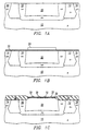
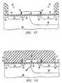
- FIGUREs 1a - 1g are a series of schematic cross-sectional diagrams illustrating the construction of one embodiment of a power transistor according to the teachings of the present invention.
- FIGUREs 1a - 1g illustrate the sequential processing steps which may be used to construct a power field effect transistor according to the teachings of the present invention.
- a p-type substrate 10 is provided that comprises a resistivity on the order of 12-16 ohm centimeters.
- the outer surface of the substrate 10 is provided with diffused regions prior to the growth of an n- epitaxial layer 12.
- the diffused regions and the outer surface of the substrate 10 are then augmented by diffusions to the outer surface of epitaxial layer 12 to provide for p+ isolation regions 14 and 16 and n+ isolation ring 18.
- Isolation regions 14, 16 and 18 isolate and define an active region 20 in which the power transistor of the present invention is formed.
- the power transistor formed in active region 20 is isolated from other devices formed on substrate 10 in epitaxial layer 12 by the isolation effects of isolation regions 14 and 16 and the junction between epitaxial layer 12 and substrate 10. Isolation ring 18 prevents the injection of holes into substrate 10 during particular loading and transient conditions for the power transistor.
- the power transistor formed in active region 20 can be used in either a source follower or common source configuration of a power circuit. This is in contrast to other devices which are not formed in isolated regions of an epitaxial layer and are thus automatically coupled to the voltage of the substrate in which they are formed. These devices may only be used in common source configurations.
- a 500-angstrom layer 22 of silicon dioxide is grown on the outer surface of epitaxial layer 12.
- a silicon nitride mask body 24 is then formed by depositing on the order of 1400 angstroms of silicon nitride and photolithographically patterning and etching the silicon nitride layer to form mask body 24 covering most of the outer surface of active region 20.
- the structure shown in FIGURE 1b is then subjected to an oxidation process which forms field oxide bodies 26 and 28 shown in FIGURE 1c.
- the silicon nitride mask body 24 is then removed as well as the remainder of layer 22.
- a series of conventional processing steps are then used to grow a 500-angstrom thick gate oxide layer 30 shown in FIGURE 1c.
- a layer of polycrystalline silicon is then deposited covering the entire structure.
- This layer is patterned and etched using conventional photolithographic processes to form an intricate gate conductor which comprises a number of gate conductor fingers 32 shown in FIGURE 1c.
- the gate conductor fingers 32 are insulated from the outer surface of active region 20 by the gate oxide 30.
- the spaces between the gate conductor fingers 32 are alternating instances of source regions and drain regions, the structure of each of which will be fully described herein.
- FIGURE 1d shows an expanded view of a single gate conductor 32.
- Gate conductor 32 has a source region indicated generally at 34 on the right side of gate conductor 32.
- a drain region indicated generally at 36 is on the left side of gate conductor 32.
- the processing of the transistor of the present invention continues by covering the drain region 36 with a photoresist mask 38 shown in FIGURE 1d.
- a D-well implant step is then used to form a D-well region 40 within source region 34.
- the D-well implant step comprises the implantation of boron ions at a dose of 4E13 ions per square centimeter and at an energy of 40 keV.
- the implanted structure is then subjected to a D-well diffusion step which comprises heating the structure at 1100 C for on the order of 12 hours. These steps result in the profile of D-well region 40 shown in FIGURE 1d. Photoresist mask 38 is then removed.
- sidewall insulator bodies 42 and 44 are formed by first depositing 3,000 angstroms of oxide using a TEOS deposition process. The 3,000 angstrom oxide is then etched anisotropically to leave sidewall insulator bodies 42 and 44. This etching process also removes the portions of gate oxide layer 30 which are not covered by gate conductor 32 or sidewall insulator bodies 42 or 44. A second TEOS deposition of 300 angstroms of oxide is then performed to form insulator layer 46 covering the device including the source region 34, drain region 36, and gate region 32.
- Regions 48 and 50 are formed by first forming a photoresist mask which is not shown to keep the n-type impurities to be implanted out of contact regions to D-well 40. The n- regions 48 and 50 are then formed using a phosphorous implant which is self-aligned to the exposed edges of insulator bodies 42 and 44. The phosphor implant is performed at dosage of 4e14 ions per square centimeter at an energy on the order 80 keV. The regions are than annealed for forty-five minutes at approximately 900 C.
- n+ source region 52 and n+ drain region 54 are formed by first forming a photoresist mask 56. An implantation of arsenic ions is then performed at a dosage of 3E15 and an energy on the order of 135 keV. The arsenic implant is then annealed for forty-five minutes at approximately 900 C. The arsenic implant is, once again, self-aligned to the exposed edges of insulator bodies 42 and 44.
- Region 58 is formed by first forming a photoresist mask 60 and then performing two boron implants.
- the first boron implant is at a dosage of 2E15 at 40 keV.
- the second boron implant is also at a dosage of 2E15 but at an energy of 120 keV. After annealing, these implants provide a contact to D-well region 40. Conventional methods may then be used to form circuit contacts to D-well contact region 58, source region 52, drain region 54 and gate conductor 32.
- the voltage on gate conductor 32 controls the conductance of a channel region indicated generally at 62. Due to the incorporation of drain region 50 and source region 48 which both comprise lightly-doped n-type regions, the device shown in FIGURE 1g enjoys a very low source-to-drain resistance when the channel region 62 is activated. In addition, because the highly-doped drain region 54 is spaced apart from the gate conductor 32 because of the use of sidewall insulator 44, the device is able to withstand a large source-to-drain voltage and drain-to-gate voltage difference without experiencing breakdown.
- the device is constructed within an active region 20 which comprises an n-type epitaxial tank constructed within a p-type substrate. For this reason, the back gate 40 is not coupled automatically to the substrate voltage. As such, the device shown in FIGURE 1g can be used in an isolated context in either a common source or a source follower driver configuration.
- an additional masking step could be used to prevent the formation of sidewall insulator body 42.
- the source-to-drain resistance could be further reduced by allowing the highly-doped source region 52 to be formed in an implantation step which was self-aligned to the right edge of gate conductor 32 as opposed to the outer edge of sidewall insulator body 42.
- This alternative embodiment includes an extra masking step to prevent the formation of sidewall insulator body 42.
- isolation regions 14 and 16 A variety of alternative methods may be used to form the isolation regions 14 and 16 described previously.
- the method described with reference to FIGURE 1a was the combination of a surface implant of p-type impurities and a buried implant formed prior to the formation of the epitaxial layer 12.
- trench isolation techniques may be used. For example, trenches can be formed through etching processes. The trenches may then be filled with oxide or other suitable insulator to provide isolation of the active region 20 from the remaining circuits.
- n-type epitaxial tank formed on a p-type substrate the invention is equally applicable to the reverse of these conductivity types.
- the same structure could be formed in a p-type epitaxial tank formed on an n-type substrate.
- the regions described as formed with n-type implantations would be formed with the opposite conductivity type.
Landscapes
- Insulated Gate Type Field-Effect Transistor (AREA)
- Element Separation (AREA)
Applications Claiming Priority (2)
| Application Number | Priority Date | Filing Date | Title |
|---|---|---|---|
| US308895P | 1995-08-31 | 1995-08-31 | |
| US3088 | 1995-08-31 |
Publications (2)
| Publication Number | Publication Date |
|---|---|
| EP0764988A2 true EP0764988A2 (de) | 1997-03-26 |
| EP0764988A3 EP0764988A3 (de) | 1998-03-04 |
Family
ID=21704082
Family Applications (1)
| Application Number | Title | Priority Date | Filing Date |
|---|---|---|---|
| EP96306319A Withdrawn EP0764988A3 (de) | 1995-08-31 | 1996-08-30 | Isolierter Leistungstransistor |
Country Status (3)
| Country | Link |
|---|---|
| US (1) | US5719423A (de) |
| EP (1) | EP0764988A3 (de) |
| KR (1) | KR100399690B1 (de) |
Cited By (3)
| Publication number | Priority date | Publication date | Assignee | Title |
|---|---|---|---|---|
| EP0880183A3 (de) * | 1997-05-23 | 1999-07-28 | Texas Instruments Incorporated | LDMOS-Leistungsanordnung |
| WO1999041780A1 (de) * | 1998-02-12 | 1999-08-19 | Siemens Aktiengesellschaft | Halbleiterbauelement mit struktur zur vermeidung von querströmen |
| EP2302677A1 (de) * | 2000-12-28 | 2011-03-30 | Canon Kabushiki Kaisha | Herstellungsverfahren für eine Halbleiteranordnung |
Families Citing this family (4)
| Publication number | Priority date | Publication date | Assignee | Title |
|---|---|---|---|---|
| KR100278661B1 (ko) * | 1998-11-13 | 2001-02-01 | 윤종용 | 비휘발성 메모리소자 및 그 제조방법 |
| US6911695B2 (en) * | 2002-09-19 | 2005-06-28 | Intel Corporation | Transistor having insulating spacers on gate sidewalls to reduce overlap between the gate and doped extension regions of the source and drain |
| JP4419699B2 (ja) * | 2004-06-16 | 2010-02-24 | ソニー株式会社 | 不揮発性半導体メモリ装置およびその動作方法 |
| JP2009521126A (ja) * | 2005-12-22 | 2009-05-28 | エヌエックスピー ビー ヴィ | フィールドプレートを具える半導体デバイス及びその製造方法 |
Family Cites Families (14)
| Publication number | Priority date | Publication date | Assignee | Title |
|---|---|---|---|---|
| JP2547729B2 (ja) * | 1986-01-16 | 1996-10-23 | 株式会社東芝 | 高耐圧パワ−集積回路 |
| KR930001894B1 (ko) * | 1989-05-16 | 1993-03-19 | 한민구 | 그루브를 가지는 전력트랜지스터 및 그 제조방법 |
| US4910160A (en) * | 1989-06-06 | 1990-03-20 | National Semiconductor Corporation | High voltage complementary NPN/PNP process |
| JPH03155638A (ja) * | 1989-11-14 | 1991-07-03 | Hitachi Ltd | 半導体集積回路装置及びその製造方法 |
| JPH03229427A (ja) * | 1990-02-05 | 1991-10-11 | Matsushita Electron Corp | Mos型半導体装置の製造方法 |
| DE69029942T2 (de) * | 1990-10-16 | 1997-08-28 | Cons Ric Microelettronica | Verfahren zur Herstellung von MOS-Leistungstransistoren mit vertikalem Strom |
| US5424567A (en) * | 1991-05-15 | 1995-06-13 | North American Philips Corporation | Protected programmable transistor with reduced parasitic capacitances and method of fabrication |
| US5306652A (en) * | 1991-12-30 | 1994-04-26 | Texas Instruments Incorporated | Lateral double diffused insulated gate field effect transistor fabrication process |
| EP0562271B1 (de) * | 1992-03-26 | 1998-01-14 | Texas Instruments Incorporated | Hochspannungstruktur mit oxydisolierter Source und RESURF-Drift-Zone in Massivsilizium |
| JP3221766B2 (ja) * | 1993-04-23 | 2001-10-22 | 三菱電機株式会社 | 電界効果トランジスタの製造方法 |
| JP3141672B2 (ja) * | 1993-09-29 | 2001-03-05 | 富士電機株式会社 | 横型電界効果トランジスタ |
| JPH07176640A (ja) * | 1993-10-26 | 1995-07-14 | Fuji Electric Co Ltd | 半導体装置の製造方法 |
| US5548147A (en) * | 1994-04-08 | 1996-08-20 | Texas Instruments Incorporated | Extended drain resurf lateral DMOS devices |
| JPH08139318A (ja) * | 1994-11-11 | 1996-05-31 | Fuji Electric Co Ltd | 横型電界効果トランジスタ |
-
1996
- 1996-08-28 US US08/697,661 patent/US5719423A/en not_active Expired - Lifetime
- 1996-08-30 EP EP96306319A patent/EP0764988A3/de not_active Withdrawn
- 1996-08-31 KR KR1019960037472A patent/KR100399690B1/ko not_active Expired - Lifetime
Cited By (4)
| Publication number | Priority date | Publication date | Assignee | Title |
|---|---|---|---|---|
| EP0880183A3 (de) * | 1997-05-23 | 1999-07-28 | Texas Instruments Incorporated | LDMOS-Leistungsanordnung |
| WO1999041780A1 (de) * | 1998-02-12 | 1999-08-19 | Siemens Aktiengesellschaft | Halbleiterbauelement mit struktur zur vermeidung von querströmen |
| US6469365B1 (en) | 1998-02-12 | 2002-10-22 | Infineon Technologies Ag | Semiconductor component with a structure for avoiding parallel-path currents and method for fabricating a semiconductor component |
| EP2302677A1 (de) * | 2000-12-28 | 2011-03-30 | Canon Kabushiki Kaisha | Herstellungsverfahren für eine Halbleiteranordnung |
Also Published As
| Publication number | Publication date |
|---|---|
| US5719423A (en) | 1998-02-17 |
| KR100399690B1 (ko) | 2004-06-04 |
| EP0764988A3 (de) | 1998-03-04 |
Similar Documents
| Publication | Publication Date | Title |
|---|---|---|
| US6160290A (en) | Reduced surface field device having an extended field plate and method for forming the same | |
| US5359219A (en) | Silicon on insulator device comprising improved substrate doping | |
| US5627097A (en) | Method for making CMOS device having reduced parasitic capacitance | |
| US6855581B2 (en) | Method for fabricating a high-voltage high-power integrated circuit device | |
| US5970329A (en) | Method of forming power semiconductor devices having insulated gate electrodes | |
| US5534447A (en) | Process for fabricating MOS LDD transistor with pocket implant | |
| EP0747966A2 (de) | Quasi-vertikaler DMOS in MOS- oder BICMOS-Verfahren mit hohem Wirkungsgrad | |
| EP0676799B1 (de) | Resurf-laterale-DMOS-Bauelemente mit erweitertem Drain | |
| US6861303B2 (en) | JFET structure for integrated circuit and fabrication method | |
| US20060011985A1 (en) | Asymmetric hetero-doped high-voltage MOSFET (AH2MOS) | |
| US5382536A (en) | Method of fabricating lateral DMOS structure | |
| US4914051A (en) | Method for making a vertical power DMOS transistor with small signal bipolar transistors | |
| US6599782B1 (en) | Semiconductor device and method of fabricating thereof | |
| EP0442296A2 (de) | Hochgeschwindigkeits-SOI-Bauelement und Herstellungsverfahren dafür | |
| US3873372A (en) | Method for producing improved transistor devices | |
| KR100368847B1 (ko) | 절연게이트반도체장치및그제조방법 | |
| US5229633A (en) | High voltage lateral enhancement IGFET | |
| KR0128501B1 (ko) | 반도체 장치 및 그 제조방법 | |
| US5719423A (en) | Isolated power transistor | |
| US5010034A (en) | CMOS and bipolar fabrication process using selective epitaxial growth scalable to below 0.5 micron | |
| US6080612A (en) | Method of forming an ultra-thin SOI electrostatic discharge protection device | |
| US7968415B2 (en) | Transistor with reduced short channel effects and method | |
| US5976924A (en) | Method of making a self-aligned disposable gate electrode for advanced CMOS design | |
| US6806541B2 (en) | Field effect transistor with improved isolation structures | |
| US6908859B2 (en) | Low leakage power transistor and method of forming |
Legal Events
| Date | Code | Title | Description |
|---|---|---|---|
| PUAI | Public reference made under article 153(3) epc to a published international application that has entered the european phase |
Free format text: ORIGINAL CODE: 0009012 |
|
| AK | Designated contracting states |
Kind code of ref document: A2 Designated state(s): DE FR GB IT NL |
|
| PUAL | Search report despatched |
Free format text: ORIGINAL CODE: 0009013 |
|
| AK | Designated contracting states |
Kind code of ref document: A3 Designated state(s): DE FR GB IT NL |
|
| 17P | Request for examination filed |
Effective date: 19980904 |
|
| AKX | Designation fees paid |
Free format text: DE FR GB IT NL |
|
| RBV | Designated contracting states (corrected) |
Designated state(s): DE FR GB IT NL |
|
| 17Q | First examination report despatched |
Effective date: 20020204 |
|
| STAA | Information on the status of an ep patent application or granted ep patent |
Free format text: STATUS: THE APPLICATION IS DEEMED TO BE WITHDRAWN |
|
| 18D | Application deemed to be withdrawn |
Effective date: 20020618 |