EP0766060A1 - Mikromechanisches Teil mit mindestens einem aus Diamant bestehendem Stift und Verfahren zu seiner Herstellung - Google Patents
Mikromechanisches Teil mit mindestens einem aus Diamant bestehendem Stift und Verfahren zu seiner Herstellung Download PDFInfo
- Publication number
- EP0766060A1 EP0766060A1 EP96402074A EP96402074A EP0766060A1 EP 0766060 A1 EP0766060 A1 EP 0766060A1 EP 96402074 A EP96402074 A EP 96402074A EP 96402074 A EP96402074 A EP 96402074A EP 0766060 A1 EP0766060 A1 EP 0766060A1
- Authority
- EP
- European Patent Office
- Prior art keywords
- diamond
- layer
- lever
- substrate
- silicon
- Prior art date
- Legal status (The legal status is an assumption and is not a legal conclusion. Google has not performed a legal analysis and makes no representation as to the accuracy of the status listed.)
- Granted
Links
Images




Classifications
-
- G—PHYSICS
- G01—MEASURING; TESTING
- G01Q—SCANNING-PROBE TECHNIQUES OR APPARATUS; APPLICATIONS OF SCANNING-PROBE TECHNIQUES, e.g. SCANNING PROBE MICROSCOPY [SPM]
- G01Q70/00—General aspects of SPM probes, their manufacture or their related instrumentation, insofar as they are not specially adapted to a single SPM technique covered by group G01Q60/00
- G01Q70/16—Probe manufacture
-
- B—PERFORMING OPERATIONS; TRANSPORTING
- B82—NANOTECHNOLOGY
- B82Y—SPECIFIC USES OR APPLICATIONS OF NANOSTRUCTURES; MEASUREMENT OR ANALYSIS OF NANOSTRUCTURES; MANUFACTURE OR TREATMENT OF NANOSTRUCTURES
- B82Y35/00—Methods or apparatus for measurement or analysis of nanostructures
-
- G—PHYSICS
- G01—MEASURING; TESTING
- G01Q—SCANNING-PROBE TECHNIQUES OR APPARATUS; APPLICATIONS OF SCANNING-PROBE TECHNIQUES, e.g. SCANNING PROBE MICROSCOPY [SPM]
- G01Q70/00—General aspects of SPM probes, their manufacture or their related instrumentation, insofar as they are not specially adapted to a single SPM technique covered by group G01Q60/00
- G01Q70/08—Probe characteristics
- G01Q70/14—Particular materials
Definitions
- the invention relates more particularly, but not exclusively, to such a method for the manufacture of a micromechanical detector for an atomic force microscope or the like.
- a process of this kind is known, in particular from US-A-5,221,415 or from EP-B-0,413,041.
- the diamond tip produced with an accuracy much less than a micron is fixed to the end of a lever whose other end is secured to a block which can be moved by appropriate means along submicrometric distances in three orthogonal directions.
- the diamond point makes it possible to explore the surface of a sample and to produce, using sensors detecting the submicrometric displacements of the end of the lever provided with the point, profiles of the topography of the surface of the sample.
- the forces that can be detected with such a lever and tip system are very low and can be of the order of nanonewton (nN).
- the spring constant k of the lever have a appropriate value of the order of 1N / m (1 newton / meter), while the resonance frequency of the lever must be relatively high, in particular at least equal to 10 kHz.
- radius of curvature of the end of the diamond point Another factor involved in the precision and sensitivity of the micromechanical detector is the radius of curvature of the end of the diamond point.
- This radius of curvature has a value of the order of 100 nm (100 nanometers), a value which it is desirable to reduce, in particular to improve the precision of surface analysis.
- the object of the invention is therefore, above all, to provide a manufacturing process which makes it possible to obtain a diamond point whose end has a radius of curvature significantly less than 100 nm and advantageously of the order of 20 nm.
- the invention also aims to provide a method for making the diamond part with the tip, under reliable and relatively economical conditions.
- the invention also aims to provide a manufacturing process which allows the lever to be produced in good conditions and to easily integrate the diamond point into the lever.
- fine diamond particles consisting of small diamond crystals, allows a regular growth of the diamond layer during vapor deposition.
- the surface density of fine diamond particles is preferably greater than 10 10 / cm 2
- Chemical vapor deposition takes place in a reactor at a temperature of around 800 ° C, in particular in the presence of a plasma composed of methane (CH 4 ) and hydrogen (H2).
- a diamond layer of the order of one micrometer is produced.
- this lever can itself be made of diamond; according to the method of the invention the primary layer of fine diamond particles is deposited over the entire surface of the imprint including that corresponding to the lever, and the lever and the point are made in one piece with diamond.
- the part comprises a lever provided with a diamond point at one end
- the lever may consist of a thin layer of a material other than the diamond of the point, this thin layer being integral with the substrate and crossed by the impression before depositing the diamond so that the diamond tip is linked to the thin layer after depositing the diamond in the impression.
- the thin layer in particular of the same material as the substrate, can be placed against a face of the substrate from which it is separated by an intermediate layer, in particular of oxide in accordance with the technology that is usually designated by "silicon on insulator ".
- this thin layer consists of a part of the substrate, in particular of silicon, in which the diamond structure has been molded.
- Said thin layer of silicon, intended to form the lever can be doped, in particular with boron, to stop the chemical attack on silicon, when removing part of the substrate.
- a circular or substantially circular window is delimited by a mask, on one face of the substrate, and by a dry attack, notably with plasma, of the substrate through this window, a shaped imprint is produced. pointed cone, in which the diamond deposit is made.
- an oxide layer can be formed by thermal oxidation on the wall of the impression, which oxide layer is then removed after depositing the diamond.
- a square window is delimited by a mask on one face of a silicon substrate and, by a wet attack on the silicon substrate, in particular by KOH, we make an inverted pyramid print (plans 111).
- the diamond layer After depositing the diamond layer, it is covered by a support structure, or a connection is established between this diamond layer and an appropriate support.
- the substrate can be made of silicon, silicon oxide or equivalent.
- the diamond layer can be made electrically conductive for certain applications, or electrically insulating for other applications.
- the invention also relates to a micromechanical part comprising a diamond point, obtained in particular by a method as defined above, this part being characterized in that the radius of curvature of the end of the diamond point is less than or equal to 20 nm (20 nanometers).
- the piece can include two, or more than two, diamond points, in particular one fine in pointed cone, the other in inverted pyramid.
- the part comprises two separate levers integral with a same base, associated respectively with each of the diamond points.
- the pyramidal tip is intended, in particular, to carry out micro-indentations on a sample, in particular for hardness measurement; the lever of the pyramidal point is generally thicker than the lever of the fine point.
- At least one piezoresistive element or a strain gauge is incorporated into the lever for measuring the mechanical stresses on this lever.
- the piezoresistive element or elements or strain gauges advantageously consist of zones of the lever (s) in silicon having undergone an appropriate treatment.
- the part is preferably attached by arms, intended to be broken, to the sides of a grid carrying several identical parts, and intended to be placed against a grid of supports of identical geometric configuration, for the connection of all the parts of a grid with all the supports of a grid, in particular by gluing or welding.
- the part is equipped with a fine point in an acute diamond cone, and this point is arranged as an electrode in a cavity of similar shape formed in a layer of suitable material to form a source of electrons.
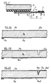
- Figure 1 of these drawings is an elevational diagram of a lever provided with a diamond point, according to the invention, fixed under a support.
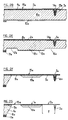
- FIGS. 2A to 2G are diagrams illustrating successive stages of the method of the invention for the manufacture of a part comprising a fine point and a diamond lever.
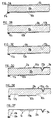
- FIGS. 3A to 3F are diagrams illustrating the steps of the method according to the invention for the manufacture of a part comprising a pyramidal point and a diamond lever.
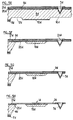
- FIGS. 4A to 4H are diagrams illustrating the successive stages of the process for the manufacture of a part comprising a fine diamond point and a silicon lever.
- FIGS. 5A to 5H are diagrams illustrating the successive stages of the method for the manufacture of a part comprising a pyramidal point in diamond and a lever in silicon.
- Figure 6 is a vertical schematic longitudinal section of a part comprising a lever and a diamond tip according to the invention, equipped with a piezo-resistance.
- Figure 7 is a schematic top view of a part comprising two separate levers integral with the same base and equipped respectively with a fine tip and a pyramidal tip, as well as strain gauges.
- Figures 8A to 8C are diagrams illustrating the assembly of micromechanical parts and supports arranged in grids.
- Figure 9 is a diagram of an electron source equipped with a fine diamond point.
- a micromechanical part 1 comprising a lever 2 (or beam) at one end of which is fixed a diamond point 3.
- the end of the lever 2 remote from the point 3 is secured to a thicker base 4, fixed under a support 5 of larger dimensions.
- Figure 1 is drawn on a very large scale, and to clarify the ideas, the orders of magnitude of the dimensions of the room are recalled below.
- the distance 1 between the end of the tip 3 and the start of the embedding area of maximum section of the base 4 is of the order of 500 ⁇ m (500 micrometers).
- the length j of the transition zone 6 where the section gradually increases between the lever 2 and the base 4 is of the order of 100 ⁇ m.
- the base 4 consists, for example, of a substantially rectangular plate of dimensions 1.6 x 3.5 mm. This base 4 may comprise, perpendicular to its short sides, several parallel levers 2 as illustrated in FIG. 7. More generally, the levers 2 have a length of between 300 and 500 ⁇ m, a width (dimension along the direction perpendicular to the plane of Figure 1) between 30 and 100 ⁇ m, and a thickness e less than 20 ⁇ m, typically 2 ⁇ m.
- the base 4 has a thickness greater than that of the lever, of the order of double, which can reach 40 ⁇ m.
- the support 5, to which the base is fixed by gluing or welding, can have a thickness of the order of 380 ⁇ m which is that of a typical silicon wafer.
- micromechanical parts are used for various applications, two of which will be cited for the record and to clarify ideas.
- a first application relates to atomic force microscopes which allow the exploration of the surface of a sample and the obtaining of high precision images, by application and displacement of the tip 3 against the surface of the sample.
- the force of application of the tip 3 against the surface is very low, of the order of a nanonewton and is obtained by the elasticity of the lever 2 forming a beam, the support 5 being moved by means of submicrometric displacements.
- the spring constant of lever 2 is chosen to be of the order of 1 N / m, and the displacement is very small.
- Displacements are measured by appropriate sensors; in particular, the lever 2 may include a reflective layer on which a laser beam is directed; the deflection of the reflected beam allows the measurement of the deformation of the lever 2 and of the displacement of the tip 3. Such a sensor detects displacements to within an angstrom.
- points 3 in the form of cones with a small angle at the top.
- the end of the tip 3 has a radius of curvature as small as possible, and less than that of the devices of the prior art.
- the tip 3 can be made electrically conductive, which makes it possible to carry out electrical measurements and to detect, for example, on the surface of the explored sample an insulating layer, zones of different conductivity and, more generally to detect certain properties of the material of the sample whose surface is explored by the tip 3.
- FIG. 1 Another application of a micromechanical part of the kind illustrated in FIG. 1 relates to a "nanoindenter” which, in the sample to be studied, indents very small dimensions (nanoindentation) with the diamond tip 3, to a measure of the hardness of the sample surface.
- the force exerted on the tip 3 is then higher than that used in the application of the atomic force microscope.
- a pyramidal point 3 that is to say in the shape of an inverted pyramid whose point is directed downwards.
- FIGS. 2A to 2G schematically illustrate the steps of the method for manufacturing a part 1a (FIG. 2G) with a fine point 3a and a lever 2a in diamond, the end of the tip 3a having a radius of curvature significantly less than 100 nm, and in particular less than or equal to 20 nm.
- a double-sided silicon wafer 8a is used, the thickness of which is for example 380 ⁇ m. Oxidation is carried out on the two faces of the wafer 8a to obtain a layer 9a, 10a of silicon oxide SiO 2 on each face.
- the thickness of the oxide layers 9a, 10a can be of the order of 7000 angstroms, while the thickness of the nitride layer is of the order of 1000 angstroms.
- the structuring of the silicon nitride and of the oxide layer 10a on the underside is carried out.
- the structuring consists in carrying out a photo-mask on the face concerned, with an appropriate resin, for tracing the outline of the zones to be preserved or removed, and then in carrying out an etching, that is to say an attack. with an appropriate product or means, to remove a certain quantity of material in the areas not protected by the photomask.
- the nitride layer is removed from the upper face and the upper oxide layer 9a is structured, with a window 12a having a circular, or substantially circular, outline towards the right end.
- the surface of the silicon wafer 8a is therefore no longer protected by the layer 9a at the level of the window 12a.
- an anisotropic dry attack of the silicon is carried out.
- Such an attack can be carried out with RIE plasma (Reactive Ion Etching or attack by reactive ions), this plasma comprising a mixture of CHF 3 , O 2 and SF 6 in proportions experimentally defined so as to have a cavity or imprint 13a (FIG. 2B) in the form of a cone whose angle at the top is about 10 °.
- RIE plasma Reactive Ion Etching or attack by reactive ions
- oxidation is carried out at low temperature and an oxide layer 14a is formed on the wall of the cavity 13a; the thickness of the layer 14a is less in the bottom so that the remaining space of the cavity 13a is more pointed after the formation of this oxide layer 14a.
- a photoresist layer is deposited on the upper Ra1 and lower Ra2 faces. The upper photoresist layer Ra1 which is then structured to define the areas where the growth of the diamond will take place.
- the process is then carried out, typically for 30 minutes, of a preparation layer composed of fine particles of diamond.
- This operation allows diamond particles, the size of which is less than 10 nm, to be deposited on the predefined area of the wafer.
- the surface density of these particles or germs is of the order of 10 10 / cm 2 .
- a chemical vapor deposition is carried out causing the diamond layer to grow in order to obtain a layer 15a (FIG. 2D).
- This layer 15a forms, continuously, the tip 3a and the lever 2a.
- the part is then taken out of the reactor and an etching operation of the oxide layer 10a and then of the silicon of the wafer 8a is carried out to make a first recess 16a in the silicon below the tip 3a, coated with the layer 14a , and a second recess 17a comprised between the zone coated with the layer 11a of silicon nitride and a central zone 18a whose lower face remains covered with the oxide layer 10a.
- etching of the oxide layer 9a is then carried out on either side of this central area 19a in order to eliminate this oxide and to release the tip 3a and the diamond layer 15a on either side of the central area 19a.
- the etching operations are carried out by chemical attack.
- a metallic layer, or a combination of metallic layers, for example a layer of titanium Ti and a layer of gold (Au) can be deposited on the upper surface of the lever and above the tip 3a.
- a metal layer makes it possible to facilitate welding or bonding of the part with a support 5 (FIG. 1) and ensures electrical contact with the diamond tip 3a.
- this metal layer can serve as a reflecting layer for detecting the displacement of the tip 3a and the deformation of the lever 2a by deflection of an optical beam, in particular a laser beam.
- FIGS. 3A to 3F illustrate the steps of the method for producing a part composed of a pyramidal point 3b (FIG. 3F) and a lever 2b made of diamond.
- FIG. 3A corresponds substantially to that of FIG. 2A and the description will not be reprise.
- the different parts are designated by the same reference numbers followed by the letter b, instead of a.
- a photolithography and etching operation is carried out on the oxide layer 9b of the upper face of the wafer 8b to determine an opening 12b, with a square outline, in the layer d 'oxide 9b.
- the silicon wafer 8b is subjected to etching or anisotropic attack with potassium hydroxide (KOH) at the level of the window 12b, at a temperature of the order of 60 ° C.
- KOH potassium hydroxide
- the progression of such an etching is of the order of 14 ⁇ m / h and it stops on planes (111) of the silicon.
- the result of this etching is shown, as illustrated in FIG. 3C, by a recess 13b in the form of an inverted pyramid with a square base, with an opening angle of 70.5 °.
- the duration of the attack depends on the size desired for the tip 3b and therefore for the recess 13b.
- an etching operation is carried out in the oxide layer 9b of the upper face to expose the silicon of the part 2b forming a lever.
- the recess 13b and the imprint corresponding to the lever 2b are placed on the wall of a primary layer of fine diamond particles, as already explained with reference to FIG. 2D, of diameter less than 10 nm, to act as germs.
- the part is introduced into the reactor for the growth of the diamond layer by vapor deposition.
- the oxide layer 9b prevents nucleation in regions other than those corresponding to the silicon surfaces released from this layer.
- the diamond layer 15b is obtained (FIG. 3D) continuously forming the tip 3b and the lever 2b.
- the etching of the oxide is continued in the central zone of the lower layer 10b and the etching of the silicon until complete drilling to reach the lever 2b.
- a central zone 19b of silicon remains corresponding to a doped zone allowing the chemical attack to be stopped at the p-n junction.
- the lever 2b associated with a pyramidal point 3b may have a thickness greater than that of a lever 2a associated with a fine point 3a, in particular due to the greater forces brought into play when it comes to carrying out a micro- indentation with the pyramidal tip 3b.
- FIGS. 4A to 4H relate to the manufacture of a part comprising a fine point 3c in diamond and a lever 2c in silicon.
- the same reference numerals, followed by the letter c instead of a, will designate the parts similar or analogous to those already described in connection with FIGS. 2A to 2G, without repeating their description in detail.
- the combination of a silicon wafer 8c is used on a face (the upper face in the case of FIG. 4A) of which a thin layer 20c of is formed.
- silicon oxide SiO 2 and on this layer 20c is deposited a layer of silicon 21c slightly thicker than the layer 20c.
- the thickness of the layer 20c is of the order of 100 nm while the thickness of the layer 21c is of the order of 2 to 20 ⁇ m.
- Oxidation is carried out on both sides leading to the layers 9c, 10c of silicon oxide.
- a deposition of silicon nitride is carried out on both sides, then the structuring of the silicon nitride and the oxide layer is carried out on the underside, which leads to the remaining part llc of silicon nitride and to the layer 10c silicon oxide shown in Figure 4A.
- the removal of the silicon nitride from the upper face and the structuring of the oxide layer 9c from the upper face are carried out.
- a photoetching of the oxide layer 9c, of the silicon layer 21c and of the oxide layer 20c is carried out so as to obtain the window 12c with a circular outline opening onto the substrate formed by the plate 8c.
- An anisotropic dry etching of the silicon of the substrate 8c is then carried out through the window 12c to obtain the conical recess 13c.
- an oxidation is carried out at low temperature ensuring the formation of an oxide layer 14c in the imprint 13c.
- a protective layer Rc of photoresist is deposited on the lower face and a protective layer 22c of photoresist on the upper face.
- the upper layer 22c of photoresist is then structured, so as to determine the contours of the unprotected zone 23c on which the subsequent diamond deposition will take place.
- the zone 23c surrounds the base of the recess 13c. The configuration obtained is that shown in FIG. 4C.
- the next step consists in depositing the primary layer of fine diamond particles, of diameter less than 10 nm, in the recess 13c and in the zone 23c. Then, the photoresist layers Rc and 22c are removed.
- the part is then introduced into the reactor for the growth of the diamond layer by vapor deposition as already explained with reference to FIG. 2D.
- the diagram of FIG. 4D where the diamond point 3c is located in the mold delimited by the oxide layer 14c in the imprint 13c.
- the tip 3c is integral with a base 24c in the form of a crown corresponding to the layer of diamond which has formed in the area 23c. This ring is linked to the part of the oxide layer 9c situated between it and the silicon layer 21c.
- the etching of the lower oxide layer 10c is continued, as well as the etching of the silicon of the substrate 8c with stopping on the oxide layer 20c, which leads to the diagram of FIG. 4F, with conservation of a central part of silicon 19c.
- the elimination is then carried out by etching of the zones of the oxide layer 20c situated on either side of the central part 19c and of the upper oxide layer 9c in the zones determined by the structuring. Then the etching of the silicon layer 21c is carried out with the oxide layer 9c as a mask, in order to obtain the desired contour of the lever 2c in silicon.
- the sectional diagram of the part at the end of these treatments is illustrated in FIG. 4G.
- FIGS. 5A to 5H relate to the manufacture of a part comprising a pyramidal point in 3d diamond fixed to the end of a lever 2d in silicon.
- the different layers placed on the substrate 8d at the start are the same as those mentioned in connection with FIG. 4A and are represented in FIG. 5A by being designated by the same reference numbers followed by the letters d.
- the operation of photolithography and etching of the oxide layer 9d, of the silicon layer 21d and of the oxide layer 20d has not yet taken place.
- FIG. 5B When this operation is completed, the diagram of FIG. 5B is obtained with a window 12d, with a square outline, ending on the upper face of the silicon substrate 8d.
- a wet etching operation (chemical attack by KOH) of the silicon is carried out in order to obtain, as in the case of FIG. 3C, a recess 13d in the form of an inverted pyramid with a square base.
- the primary layer of fine particles of diamond is then deposited on the internal surface of the imprint 13d and the part is introduced into the reactor for the growth of the diamond layer by deposition in vapor phase, as explained in connection with figure 2D.
- the diamond tip 3d is formed in the imprint 13d, this pyramidal tip 3d being fixed at its base in the layer 21d of silicon.
- FIGS 5E and 5F correspond to the processing explained with reference to Figures 4E and 4F.
- the part is then subjected to an etching of the oxide layer 9d and to an etching of the layer 21d of silicon in the extreme part situated to the right of the tip 13d.
- the diagram at the end of this operation is that of FIG. 5G.
- the etching of the oxide layer 9d is finished, in order to eliminate it completely, and the etching of the oxide layer 20d on either side of the central silicon part 19d which remains.
- the 3d pyramidal tip has four faces with an opening angle of 70.5 °, and constitutes the replica of a pyramid obtained by anisotropic attack in crystalline silicon, and delimited by planes (111) .
- the diamond coating forming the pyramid can be made conductive by doping, preferably by boron doping incorporated during the deposition phase.
- the electrical conductivity has the advantage of avoiding electro-static forces that might otherwise interfere during measurements.
- the conductivity also makes it possible to detect the state of contact with the sample or with a conductive part situated under an insulating surface layer of the sample.
- the lever 2e may contain a strain gauge 27e formed by a piezo-resistance, situated at the end of the lever remote from the tip 3e and close to the embedding zone of this lever 2nd in the base.
- This gauge 27e is provided on the side of the upper face of the lever 2e and is preferably constituted by crystalline silicon which is particularly suitable for this function because of its superior mechanical properties, and its very sensitive piezoresistive response.
- the strain gauge 27e is protected by an insulating layer 28e; a contact layer 29e is placed on the protective layer 28e which it crosses at 30e to establish contact with the gauge 27e.
- the layer 29e also provides protection against light.
- the part formed by the lever 2e and the conical tip 3e of FIG. 6 is more particularly intended for the measurement of topographic profiles of a surface.
- a part formed by a lever 2f and a fine tip 3f (FIG. 7) of the kind described with reference to FIGS. 2G and 4H is integrated on the same plate 4e as that of the lever 2e.
- the two levers 2e, 2f integrated on the same plate 4e are parallel, cantilevered from a zone of embedding in the plate 4e.
- the distance m between the axes of the levers 2e, 2f is of the order of 100 ⁇ m.
- the contours of the levers 2e, 2f seen in plan are rectangular with parallel longitudinal edges; in the case of lever 2e, the corners of the outer end are cut down.
- a free space 31 exists between the two longitudinal edges adjacent to the levers 2e, 2f.
- An opening 32 for example with a rectangular outline, is provided in the vicinity of the recessed base of the lever 2f, along its axis, to increase the sensitivity to torsion of the beam formed by this lever 2f.
- two strain gauges 27f, 27f ' are integrated in the vicinity of the base of the lever 2f, in a similar manner to the gauge 27e, on each side of opening 32.
- a conductive track 33f in particular obtained by doping the silicon substrate of the lever 2f, is provided along the longitudinal axis of the lever to connect the tip 3f, electrically conductive, to measuring means; the track 33f bypasses the opening 32 along a rectangular perimeter.
- Similar conductive tracks 33e can be provided on the lever 2e to connect a conductive tip 3e to measuring means.
- the 4th plate includes a reference gauge 34e which makes it possible to compensate for the temperature variations at the level of the measurements carried out with the piezo-resistance strain gauges 27e, 27f and 27f '.
- gauge 27e of the lever 2e is arranged along its axis, for the measurements in bending.
- the lever 2e has dimensions, in particular a thickness, greater than those of the lever 2f because it uses greater forces.
- the lever 2f with fine tip 3f makes it possible to produce images by atomic force microscopy of the surface of the sample and indentations carried out with the tip 3e.
- the lever 2f also makes it possible to directly measure the depth of the indentation produced with the tip 3e during its production.
- the reference gauges can be integrated on the plate 4e, or they can be projecting as illustrated in figure 7. This second option makes it possible to create cooling conditions strain gauges similar to those of the measurement levers.
- P + regions are created for the electrical contacts of the piezoresistors.
- N + regions are defined for electrical contact with the substrate.
- the conductive tracks making it possible to establish the electrical connections between the tips and the resistances of the strain gauges with the measuring devices can also be produced by depositing conductive metallic layers.
- the points 3f and 3e are produced sequentially, the fine point 3f first then the pyramidal point 3e.
- the combination of the two points 3e and 3f on levers embedded on the same plate 4e has the advantage of allowing the measurement of the depth of the indentation by measuring the difference in flexions of the two levers 2e, 2f during an indentation.
- the two levers 2e, 2f can be produced either simultaneously from the same plate 4e, or else separately, to then be joined together on the same plate 4e.
- each support 5 is located inside a rectangular empty cell 35 delimited by branches 36, 37 of a grid 38 forming a support frame.
- the representation of FIG. 8A is at greatly enlarged scale, the dimensions of cell 35 being of the order of 5 mm x 8 mm.
- the support 5, already described with reference to FIG. 1, has a rectangular shape with cut corners, the length of which is arranged parallel to the long sides of the cell 35.
- the centers of the support 5 and of the cell 35 coincide.
- the long sides of the support 5 are connected to the longitudinal branches 37 by arms 39 having a reduced-size area 40 at the junction of the support 5 to facilitate, by rupture, the separation between the support 5 and the arms 39.
- the two arms 39 located on either side of the support 5 are in the extension of one another, parallel to the small branches 36 of the grid and are offset on one side, to the left according to FIG. 8A, relative to the mediator of the long sides of the cell 35.
- FIG. 8A shows, inside the contour of the support 5, by a darker area the surface provided with glue or solder for fixing, to the support 5, the plate 4 illustrated in FIG. 8B.
- the plate 4, already described with reference to FIG. 1, has an outline similar to that of the support 5.
- Several levers such as 2, 2h (see FIG. 6) or 2g protrude from the short sides of the plate 4, according to a direction perpendicular to this short side.
- the lever 2g has a V shape and has two arms joining at the tip of the V where the diamond tip is located, while the opposite ends of these arms are embedded in the plate 4; such a 2g two-arm lever gives better torsional stability.
- the plate 4 is located in an empty cell 35a similar to the cell 35 in FIG. 8A, located inside a grid 38a whose branches 36a, 37a surround the plate 4 at a distance.
- the latter is connected, at the level from its long sides, to arms 39a narrower and thinner than the arms 39 of FIG. 8A.
- the arms 39a are offset to the right of FIG. 8B with respect to the perpendicular bisector of the longitudinal branches 37a. Breaking zones 40a are provided at the junction of the arms 39a and the long sides of the plate 4.
- FIG. 8C shows, by dashed lines inside the contour of the support 5, the surface provided with glue or solder for fixing, to the support 5, the plate 4 illustrated in FIG. 8B.
- each plate 4 When the connection is established by taking the glue or the solder, between each plate 4 and its corresponding support 5, it is possible, by separating the grids 38 and 38a, to cause the arms 39a of weaker strength to break, and to obtain a grid 38 comprising, inside each cell 35, a support 5 to which a plate 4 is fixed. Each support 5 can then be removed individually from its cell 35 by breaking the arms 39.
- Figure 9 shows a 1h piece with a fine diamond tip 3h constituting a new type of electron source.
- the tip 3h is of the same kind as the fine tips 3a, 3c previously described and constitutes a cathode.
- the n-type layer of the substrate 8h of p-type silicon and the cavity 13h forming the mold are defined in such a way that the pn junction making it possible to stop the etching or electrochemical attack is at a level s located in the vicinity or above (as shown in Figure 9) the end q of the tip 3h.
- a p-doped layer 41 is implanted on the surface of the substrate 8 h at level s to serve as an electrode p-type extraction.
- a positive voltage applied between the extraction electrode and the diamond tip 3h (cathode) makes it possible to extract an electron current from this tip.
- the tip 3h is electrically conductive and the contact electrode 42, shown in Figure 9, is located on the side opposite the end q.
Landscapes
- Physics & Mathematics (AREA)
- Health & Medical Sciences (AREA)
- General Health & Medical Sciences (AREA)
- General Physics & Mathematics (AREA)
- Nuclear Medicine, Radiotherapy & Molecular Imaging (AREA)
- Radiology & Medical Imaging (AREA)
- Chemical & Material Sciences (AREA)
- Engineering & Computer Science (AREA)
- Nanotechnology (AREA)
- Analytical Chemistry (AREA)
- Crystallography & Structural Chemistry (AREA)
- Micromachines (AREA)
Applications Claiming Priority (2)
| Application Number | Priority Date | Filing Date | Title |
|---|---|---|---|
| FR9511490A FR2739494B1 (fr) | 1995-09-29 | 1995-09-29 | Procede de fabrication de pieces de micromecanique ayant une partie en diamant constituee au moins d'une pointe, et pieces de micromecanique comportant au moins une pointe en diamant |
| FR9511490 | 1995-09-29 |
Publications (2)
| Publication Number | Publication Date |
|---|---|
| EP0766060A1 true EP0766060A1 (de) | 1997-04-02 |
| EP0766060B1 EP0766060B1 (de) | 2002-08-14 |
Family
ID=9483082
Family Applications (1)
| Application Number | Title | Priority Date | Filing Date |
|---|---|---|---|
| EP96402074A Expired - Lifetime EP0766060B1 (de) | 1995-09-29 | 1996-09-27 | Herstellung eines mikromechanischen Teils mit mindestens einer Diamantspitze. |
Country Status (4)
| Country | Link |
|---|---|
| US (1) | US5994160A (de) |
| EP (1) | EP0766060B1 (de) |
| DE (1) | DE69622954D1 (de) |
| FR (1) | FR2739494B1 (de) |
Cited By (2)
| Publication number | Priority date | Publication date | Assignee | Title |
|---|---|---|---|---|
| EP0882944A1 (de) * | 1997-06-05 | 1998-12-09 | CSEM Centre Suisse d'Electronique et de Microtechnique | Verfahren zur Herstellung einer micromechanischen Messsonde, insbesondere eines Rasterkraftmikroskops |
| WO2008096901A1 (en) * | 2007-02-07 | 2008-08-14 | Canon Kabushiki Kaisha | Cantilever type oscillating optical deflector with mechanical guiding features |
Families Citing this family (32)
| Publication number | Priority date | Publication date | Assignee | Title |
|---|---|---|---|---|
| DE19718618C2 (de) * | 1997-05-02 | 1999-12-02 | Daimler Chrysler Ag | Komposit-Struktur mit einem mehrere mikroelektronische Bauteile und eine Diamantschicht aufweisenden Wachstums-Substrat sowie Verfahren zur Herstellung der Komposit-Struktur |
| TW374197B (en) * | 1997-12-11 | 1999-11-11 | Ind Tech Res Inst | Manufacturing process of integrated micro-flow control module |
| US6583063B1 (en) | 1998-12-03 | 2003-06-24 | Applied Materials, Inc. | Plasma etching of silicon using fluorinated gas mixtures |
| US6235214B1 (en) * | 1998-12-03 | 2001-05-22 | Applied Materials, Inc. | Plasma etching of silicon using fluorinated gas mixtures |
| US6312616B1 (en) | 1998-12-03 | 2001-11-06 | Applied Materials, Inc. | Plasma etching of polysilicon using fluorinated gas mixtures |
| US6400166B2 (en) * | 1999-04-15 | 2002-06-04 | International Business Machines Corporation | Micro probe and method of fabricating same |
| EP1111331A1 (de) * | 1999-12-23 | 2001-06-27 | C.S.E.M. Centre Suisse D'electronique Et De Microtechnique Sa | Taststift für die Nanotechnologie sowie Verfahren zu seiner Herstellung |
| DE10003836C2 (de) * | 2000-01-28 | 2002-04-25 | Fraunhofer Ges Forschung | Indentor und Verwendung desselben |
| US6583412B2 (en) * | 2000-03-17 | 2003-06-24 | University Of Utah Research Foundation | Scanning tunneling charge transfer microscope |
| US6422077B1 (en) * | 2000-04-06 | 2002-07-23 | The University Of Chicago | Ultrananocrystalline diamond cantilever wide dynamic range acceleration/vibration/pressure sensor |
| US6592519B1 (en) * | 2000-04-28 | 2003-07-15 | Medtronic, Inc. | Smart microfluidic device with universal coating |
| US7115523B2 (en) * | 2000-05-22 | 2006-10-03 | Applied Materials, Inc. | Method and apparatus for etching photomasks |
| US6391790B1 (en) | 2000-05-22 | 2002-05-21 | Applied Materials, Inc. | Method and apparatus for etching photomasks |
| US6905614B1 (en) | 2000-05-24 | 2005-06-14 | Active Optical Networks, Inc. | Pattern-transfer process for forming micro-electro-mechanical structures |
| US6827866B1 (en) * | 2000-05-24 | 2004-12-07 | Active Optical Networks, Inc. | Deep-well lithography process for forming micro-electro-mechanical structures |
| JP4610811B2 (ja) * | 2000-09-15 | 2011-01-12 | アイメック | プローブの製造方法及びその装置 |
| ATE429626T1 (de) * | 2000-09-15 | 2009-05-15 | Imec Inter Uni Micro Electr | Verfahren zur herstellung montierter afm-sonden durch löten |
| WO2002028766A2 (en) * | 2000-10-03 | 2002-04-11 | Honeywell International Inc. | Method of trimming micro-machined electromechanical sensors (mems) devices |
| TW480621B (en) | 2001-03-02 | 2002-03-21 | Acer Comm & Multimedia Inc | Method for producing high density chip |
| US7183201B2 (en) | 2001-07-23 | 2007-02-27 | Applied Materials, Inc. | Selective etching of organosilicate films over silicon oxide stop etch layers |
| CN1599939B (zh) * | 2002-01-15 | 2010-08-11 | 国际商业机器公司 | 形成微观结构的方法 |
| KR20040012451A (ko) * | 2002-05-14 | 2004-02-11 | 어플라이드 머티어리얼스, 인코포레이티드 | 포토리소그래픽 레티클을 에칭하는 방법 |
| SG101537A1 (en) * | 2002-06-03 | 2004-01-30 | Sensfab Pte Ltd | Method of forming atomic force microscope tips |
| WO2004029733A2 (fr) * | 2002-09-25 | 2004-04-08 | Fore Eagle Co Ltd | Pieces mecaniques |
| US7541219B2 (en) * | 2004-07-02 | 2009-06-02 | Seagate Technology Llc | Integrated metallic contact probe storage device |
| US8293430B2 (en) | 2005-01-27 | 2012-10-23 | Applied Materials, Inc. | Method for etching a molybdenum layer suitable for photomask fabrication |
| US8048789B2 (en) * | 2005-04-26 | 2011-11-01 | Northwestern University | Mesoscale pyramids, arrays and methods of preparation |
| WO2007070745A2 (en) * | 2005-12-01 | 2007-06-21 | Mynosys Cellular Devices, Inc. | Micro surgical cutting instruments |
| WO2007092852A2 (en) | 2006-02-06 | 2007-08-16 | Mynosys Cellular Devices, Inc. | Microsurgical cutting instruments |
| WO2009012180A1 (en) * | 2007-07-13 | 2009-01-22 | Advanced Diamond Technologies, Inc. | Ultrananocrystalline diamond film deposition for spm probes |
| US8740209B2 (en) * | 2012-02-22 | 2014-06-03 | Expresslo Llc | Method and apparatus for ex-situ lift-out specimen preparation |
| US9038269B2 (en) * | 2013-04-02 | 2015-05-26 | Xerox Corporation | Printhead with nanotips for nanoscale printing and manufacturing |
Citations (8)
| Publication number | Priority date | Publication date | Assignee | Title |
|---|---|---|---|---|
| EP0413041A1 (de) * | 1989-08-16 | 1991-02-20 | International Business Machines Corporation | Verfahren für die Herstellung mikromechanischer Messfühler für AFM/STM-Profilometrie und mikromechanischer Messfühlerkopf |
| JPH04274151A (ja) * | 1991-02-28 | 1992-09-30 | Toshiba Corp | カンチレバ−およびその製法 |
| JPH04321596A (ja) * | 1991-04-22 | 1992-11-11 | Toyota Central Res & Dev Lab Inc | ダイヤモンド膜の形成方法 |
| DE4232886A1 (de) * | 1991-09-30 | 1993-04-08 | Kobe Steel Ltd | Kaltkathoden-emitterelement |
| US5204210A (en) * | 1990-12-07 | 1993-04-20 | Xerox Corporation | Method for the direct patterning of diamond films |
| US5221415A (en) * | 1989-01-17 | 1993-06-22 | Board Of Trustees Of The Leland Stanford Junior University | Method of forming microfabricated cantilever stylus with integrated pyramidal tip |
| JPH05203444A (ja) * | 1992-01-29 | 1993-08-10 | Seiko Instr Inc | 原子間力顕微鏡用カンチレバーの製造方法 |
| DE4314301C1 (de) * | 1993-04-30 | 1994-05-05 | Imm Inst Mikrotech | Abtastvorrichtung zur Untersuchung von Oberflächenstrukturen mit Auflösung im submicron-Bereich und Verfahren zu deren Herstellung |
Family Cites Families (6)
| Publication number | Priority date | Publication date | Assignee | Title |
|---|---|---|---|---|
| US3888708A (en) * | 1972-02-17 | 1975-06-10 | Kensall D Wise | Method for forming regions of predetermined thickness in silicon |
| US5066358A (en) * | 1988-10-27 | 1991-11-19 | Board Of Trustees Of The Leland Stanford Juninor University | Nitride cantilevers with single crystal silicon tips |
| US5021286A (en) * | 1989-08-10 | 1991-06-04 | Nhk Spring Co., Ltd. | Cushion material and method of manufacturing the same |
| EP0413042B1 (de) * | 1989-08-16 | 1992-12-16 | International Business Machines Corporation | Verfahren für die Herstellung mikromechanischer Messfühler für AFM/STM-Profilometrie und mikromechanischer Messfühlerkopf |
| US5619093A (en) * | 1995-03-31 | 1997-04-08 | The United States Of America As Represented By The Secretary Of The Navy | Electron field emission |
| JPH08313541A (ja) * | 1995-05-16 | 1996-11-29 | Olympus Optical Co Ltd | 走査型プローブ顕微鏡用カンチレバー及びその製造方法 |
-
1995
- 1995-09-29 FR FR9511490A patent/FR2739494B1/fr not_active Expired - Fee Related
-
1996
- 1996-09-27 US US08/723,232 patent/US5994160A/en not_active Expired - Lifetime
- 1996-09-27 DE DE69622954T patent/DE69622954D1/de not_active Expired - Lifetime
- 1996-09-27 EP EP96402074A patent/EP0766060B1/de not_active Expired - Lifetime
Patent Citations (8)
| Publication number | Priority date | Publication date | Assignee | Title |
|---|---|---|---|---|
| US5221415A (en) * | 1989-01-17 | 1993-06-22 | Board Of Trustees Of The Leland Stanford Junior University | Method of forming microfabricated cantilever stylus with integrated pyramidal tip |
| EP0413041A1 (de) * | 1989-08-16 | 1991-02-20 | International Business Machines Corporation | Verfahren für die Herstellung mikromechanischer Messfühler für AFM/STM-Profilometrie und mikromechanischer Messfühlerkopf |
| US5204210A (en) * | 1990-12-07 | 1993-04-20 | Xerox Corporation | Method for the direct patterning of diamond films |
| JPH04274151A (ja) * | 1991-02-28 | 1992-09-30 | Toshiba Corp | カンチレバ−およびその製法 |
| JPH04321596A (ja) * | 1991-04-22 | 1992-11-11 | Toyota Central Res & Dev Lab Inc | ダイヤモンド膜の形成方法 |
| DE4232886A1 (de) * | 1991-09-30 | 1993-04-08 | Kobe Steel Ltd | Kaltkathoden-emitterelement |
| JPH05203444A (ja) * | 1992-01-29 | 1993-08-10 | Seiko Instr Inc | 原子間力顕微鏡用カンチレバーの製造方法 |
| DE4314301C1 (de) * | 1993-04-30 | 1994-05-05 | Imm Inst Mikrotech | Abtastvorrichtung zur Untersuchung von Oberflächenstrukturen mit Auflösung im submicron-Bereich und Verfahren zu deren Herstellung |
Non-Patent Citations (4)
| Title |
|---|
| GERMANN G J ET AL: "DIAMOND FORCE MICROSCOPE TIPS FABRICATED BY CHEMICAL VAPOR DEPOSITION", REVIEW OF SCIENTIFIC INSTRUMENTS, vol. 63, no. 9, 1 September 1992 (1992-09-01), pages 4053 - 4055, XP000311657 * |
| PATENT ABSTRACTS OF JAPAN vol. 017, no. 071 (E - 1319) 12 February 1993 (1993-02-12) * |
| PATENT ABSTRACTS OF JAPAN vol. 017, no. 158 (C - 1041) 29 March 1993 (1993-03-29) * |
| PATENT ABSTRACTS OF JAPAN vol. 017, no. 626 (P - 1647) 18 November 1993 (1993-11-18) * |
Cited By (5)
| Publication number | Priority date | Publication date | Assignee | Title |
|---|---|---|---|---|
| EP0882944A1 (de) * | 1997-06-05 | 1998-12-09 | CSEM Centre Suisse d'Electronique et de Microtechnique | Verfahren zur Herstellung einer micromechanischen Messsonde, insbesondere eines Rasterkraftmikroskops |
| FR2764441A1 (fr) * | 1997-06-05 | 1998-12-11 | Suisse Electronique Microtech | Procede de fabrication d'un organe palpeur pour capteur micromecanique, notamment pour microscope a force atomique |
| US6056887A (en) * | 1997-06-05 | 2000-05-02 | C.S.E.M. - Centre Suisse D'electronique Et De Microtechniques S.A. | Process for fabricating a feeler member for a micromechanical probe, in particular for an atomic force microscope |
| WO2008096901A1 (en) * | 2007-02-07 | 2008-08-14 | Canon Kabushiki Kaisha | Cantilever type oscillating optical deflector with mechanical guiding features |
| US8254004B2 (en) | 2007-02-07 | 2012-08-28 | Canon Kabushiki Kaisha | Oscillator and optical deflector having oscillator |
Also Published As
| Publication number | Publication date |
|---|---|
| DE69622954D1 (de) | 2002-09-19 |
| EP0766060B1 (de) | 2002-08-14 |
| US5994160A (en) | 1999-11-30 |
| FR2739494B1 (fr) | 1997-11-14 |
| FR2739494A1 (fr) | 1997-04-04 |
Similar Documents
| Publication | Publication Date | Title |
|---|---|---|
| EP0766060B1 (de) | Herstellung eines mikromechanischen Teils mit mindestens einer Diamantspitze. | |
| EP2309559B1 (de) | Piezoelektrische Erregerstruktur mit integriertem piezoresistivem Dehnmessstreifen und Herstellungsverfahren dafür | |
| EP0267069B1 (de) | Verfahren zur Herstellung eines Dehnungsmessstreifens mit Piezowiderstand, sowie eines Beschleunigungsmessers mit einem solchen Dehnungsmessstreifen | |
| EP2396636B1 (de) | Kontaktkraftsensor | |
| US6337477B1 (en) | Probe having micro-projection and manufacturing method thereof | |
| EP3599469B1 (de) | Beschleunigungssensor mit dehnungsmessstreifen mit verbesserter präzision | |
| EP0596456A1 (de) | Methode zur Herstellung eines integrierten kapazitiven Transduktors | |
| EP2599745B1 (de) | Verfahren zum Herstellen eines MEMS Bauteil mit bewegliche Teile unterschiedlicher Dicke | |
| FR2534022A1 (fr) | Procede de production d'un element sensible a une contrainte, dispositif pour convertir un mouvement mecanique en signaux electriques et transducteur | |
| FR2977319A1 (fr) | Dispositif de mesure de pression a sensiblite optimisee | |
| EP2491406A1 (de) | Sensor für piezoresistive detektion auf gleicher ebene | |
| EP2681568A1 (de) | Verfahren zur herstellung eines trägheitssensors | |
| EP2776364B1 (de) | Verbessertes verfahren zur herstellung einer vorrichtung mit hohlräumen zwischen einem aufgehängten element auf in einem substrat halbvergrabenen isolierenden pads und dieses substrat | |
| WO2010146138A1 (fr) | Procede de realisation d'une membrane plane | |
| EP3076897B1 (de) | System zur bestimmung der kontaktfläche und der verteilung von okklusionskräften zwischen den zähnen eines patientenkiefers und zugehöriges verfahren | |
| FR2897937A1 (fr) | Capteur de pression a jauges resistives | |
| TW201122412A (en) | Coating apparatus and method for real-time monitoring thickness change of coating film | |
| EP0882944B1 (de) | Verfahren zur Herstellung einer micromechanischen Messsonde, insbesondere eines Rasterkraftmikroskops | |
| FR2885410A1 (fr) | Dispositif de mesure de force par detection capacitive | |
| EP1050740A2 (de) | Verfahren zur integrierten Herstellung von an einer Halterung befestigten Spitzen | |
| EP3843294A1 (de) | Lichtquelle zur emission von in der polarisation verschränkten photonenpaaren | |
| FR2859281A1 (fr) | Protection d'une membrane deformable contre de fortes deformations dans une structure micromecanique | |
| WO2024194446A1 (fr) | Pointe en silicium de faible masse et à haut rapport d'aspect, sonde comportant une telle pointe en silicium, microscope comportant une telle sonde, et procédé de fabrication de ladite pointe en silicium | |
| FR2947628A1 (fr) | Procede de fabrication d'une jauge de deformation en circuit integre | |
| EP2090877A2 (de) | Mikrohebel mit eingebautem Magnetoimpedanz-Anspannungssensor |
Legal Events
| Date | Code | Title | Description |
|---|---|---|---|
| PUAI | Public reference made under article 153(3) epc to a published international application that has entered the european phase |
Free format text: ORIGINAL CODE: 0009012 |
|
| AK | Designated contracting states |
Kind code of ref document: A1 Designated state(s): CH DE FR GB LI |
|
| 17P | Request for examination filed |
Effective date: 19970805 |
|
| 17Q | First examination report despatched |
Effective date: 19981116 |
|
| GRAG | Despatch of communication of intention to grant |
Free format text: ORIGINAL CODE: EPIDOS AGRA |
|
| RTI1 | Title (correction) |
Free format text: MANUFACTURING A MICROMECHANICAL PART HAVING AT LEAST ONE TIP OF DIAMOND. |
|
| GRAG | Despatch of communication of intention to grant |
Free format text: ORIGINAL CODE: EPIDOS AGRA |
|
| GRAH | Despatch of communication of intention to grant a patent |
Free format text: ORIGINAL CODE: EPIDOS IGRA |
|
| GRAH | Despatch of communication of intention to grant a patent |
Free format text: ORIGINAL CODE: EPIDOS IGRA |
|
| GRAA | (expected) grant |
Free format text: ORIGINAL CODE: 0009210 |
|
| RAP1 | Party data changed (applicant data changed or rights of an application transferred) |
Owner name: CSEM CENTRE SUISSE D'ELECTRONIQUE ET DE MICROTECHN |
|
| AK | Designated contracting states |
Kind code of ref document: B1 Designated state(s): CH DE FR GB LI |
|
| REG | Reference to a national code |
Ref country code: GB Ref legal event code: FG4D Free format text: NOT ENGLISH |
|
| REG | Reference to a national code |
Ref country code: CH Ref legal event code: EP |
|
| REF | Corresponds to: |
Ref document number: 69622954 Country of ref document: DE Date of ref document: 20020919 |
|
| PG25 | Lapsed in a contracting state [announced via postgrant information from national office to epo] |
Ref country code: DE Free format text: LAPSE BECAUSE OF FAILURE TO SUBMIT A TRANSLATION OF THE DESCRIPTION OR TO PAY THE FEE WITHIN THE PRESCRIBED TIME-LIMIT Effective date: 20021115 |
|
| GBT | Gb: translation of ep patent filed (gb section 77(6)(a)/1977) |
Effective date: 20021031 |
|
| PLBE | No opposition filed within time limit |
Free format text: ORIGINAL CODE: 0009261 |
|
| STAA | Information on the status of an ep patent application or granted ep patent |
Free format text: STATUS: NO OPPOSITION FILED WITHIN TIME LIMIT |
|
| 26N | No opposition filed |
Effective date: 20030515 |
|
| REG | Reference to a national code |
Ref country code: GB Ref legal event code: 732E |
|
| REG | Reference to a national code |
Ref country code: CH Ref legal event code: NV Representative=s name: GLN S.A. |
|
| REG | Reference to a national code |
Ref country code: CH Ref legal event code: PCAR Free format text: NEW ADDRESS: AVENUE EDOUARD-DUBOIS 20, 2000 NEUCHATEL (CH) |
|
| PGFP | Annual fee paid to national office [announced via postgrant information from national office to epo] |
Ref country code: CH Payment date: 20140929 Year of fee payment: 19 |
|
| PGFP | Annual fee paid to national office [announced via postgrant information from national office to epo] |
Ref country code: GB Payment date: 20140929 Year of fee payment: 19 Ref country code: FR Payment date: 20140917 Year of fee payment: 19 |
|
| REG | Reference to a national code |
Ref country code: CH Ref legal event code: PL |
|
| GBPC | Gb: european patent ceased through non-payment of renewal fee |
Effective date: 20150927 |
|
| REG | Reference to a national code |
Ref country code: FR Ref legal event code: ST Effective date: 20160531 |
|
| PG25 | Lapsed in a contracting state [announced via postgrant information from national office to epo] |
Ref country code: GB Free format text: LAPSE BECAUSE OF NON-PAYMENT OF DUE FEES Effective date: 20150927 Ref country code: LI Free format text: LAPSE BECAUSE OF NON-PAYMENT OF DUE FEES Effective date: 20150930 Ref country code: CH Free format text: LAPSE BECAUSE OF NON-PAYMENT OF DUE FEES Effective date: 20150930 |
|
| PG25 | Lapsed in a contracting state [announced via postgrant information from national office to epo] |
Ref country code: FR Free format text: LAPSE BECAUSE OF NON-PAYMENT OF DUE FEES Effective date: 20150930 |