EP0766383A2 - Dispositif à ondes acoustiques de surface à diamant-ZnO comportant une couche relativement mince de ZnO piézoélectrique - Google Patents
Dispositif à ondes acoustiques de surface à diamant-ZnO comportant une couche relativement mince de ZnO piézoélectrique Download PDFInfo
- Publication number
- EP0766383A2 EP0766383A2 EP96115405A EP96115405A EP0766383A2 EP 0766383 A2 EP0766383 A2 EP 0766383A2 EP 96115405 A EP96115405 A EP 96115405A EP 96115405 A EP96115405 A EP 96115405A EP 0766383 A2 EP0766383 A2 EP 0766383A2
- Authority
- EP
- European Patent Office
- Prior art keywords
- layer
- saw
- point
- given
- thickness
- Prior art date
- Legal status (The legal status is an assumption and is not a legal conclusion. Google has not performed a legal analysis and makes no representation as to the accuracy of the status listed.)
- Granted
Links
- 238000010897 surface acoustic wave method Methods 0.000 title claims abstract description 314
- 229910003460 diamond Inorganic materials 0.000 claims abstract description 70
- 239000010432 diamond Substances 0.000 claims abstract description 70
- 229910052799 carbon Inorganic materials 0.000 claims abstract description 12
- VYPSYNLAJGMNEJ-UHFFFAOYSA-N Silicium dioxide Chemical compound O=[Si]=O VYPSYNLAJGMNEJ-UHFFFAOYSA-N 0.000 claims description 138
- 229910052681 coesite Inorganic materials 0.000 claims description 69
- 229910052906 cristobalite Inorganic materials 0.000 claims description 69
- 239000000377 silicon dioxide Substances 0.000 claims description 69
- 229910052682 stishovite Inorganic materials 0.000 claims description 69
- 229910052905 tridymite Inorganic materials 0.000 claims description 69
- 229910052782 aluminium Inorganic materials 0.000 claims description 12
- XAGFODPZIPBFFR-UHFFFAOYSA-N aluminium Chemical compound [Al] XAGFODPZIPBFFR-UHFFFAOYSA-N 0.000 claims description 12
- 239000000463 material Substances 0.000 description 20
- 230000000052 comparative effect Effects 0.000 description 10
- 230000007423 decrease Effects 0.000 description 10
- 238000000034 method Methods 0.000 description 8
- 238000004544 sputter deposition Methods 0.000 description 7
- 230000008878 coupling Effects 0.000 description 6
- 238000010168 coupling process Methods 0.000 description 6
- 238000005859 coupling reaction Methods 0.000 description 6
- 239000010408 film Substances 0.000 description 6
- 238000005259 measurement Methods 0.000 description 6
- 239000000758 substrate Substances 0.000 description 6
- 238000003780 insertion Methods 0.000 description 5
- 230000037431 insertion Effects 0.000 description 5
- 230000008859 change Effects 0.000 description 4
- 239000007789 gas Substances 0.000 description 4
- 238000004519 manufacturing process Methods 0.000 description 4
- 238000005457 optimization Methods 0.000 description 4
- 230000008569 process Effects 0.000 description 4
- VZSRBBMJRBPUNF-UHFFFAOYSA-N 2-(2,3-dihydro-1H-inden-2-ylamino)-N-[3-oxo-3-(2,4,6,7-tetrahydrotriazolo[4,5-c]pyridin-5-yl)propyl]pyrimidine-5-carboxamide Chemical compound C1C(CC2=CC=CC=C12)NC1=NC=C(C=N1)C(=O)NCCC(N1CC2=C(CC1)NN=N2)=O VZSRBBMJRBPUNF-UHFFFAOYSA-N 0.000 description 3
- AFCARXCZXQIEQB-UHFFFAOYSA-N N-[3-oxo-3-(2,4,6,7-tetrahydrotriazolo[4,5-c]pyridin-5-yl)propyl]-2-[[3-(trifluoromethoxy)phenyl]methylamino]pyrimidine-5-carboxamide Chemical compound O=C(CCNC(=O)C=1C=NC(=NC=1)NCC1=CC(=CC=C1)OC(F)(F)F)N1CC2=C(CC1)NN=N2 AFCARXCZXQIEQB-UHFFFAOYSA-N 0.000 description 3
- 229910021486 amorphous silicon dioxide Inorganic materials 0.000 description 3
- 238000000206 photolithography Methods 0.000 description 3
- 238000004891 communication Methods 0.000 description 2
- 230000000694 effects Effects 0.000 description 2
- 238000011156 evaluation Methods 0.000 description 2
- 238000012986 modification Methods 0.000 description 2
- 230000004048 modification Effects 0.000 description 2
- 238000005240 physical vapour deposition Methods 0.000 description 2
- 238000005268 plasma chemical vapour deposition Methods 0.000 description 2
- YLZOPXRUQYQQID-UHFFFAOYSA-N 3-(2,4,6,7-tetrahydrotriazolo[4,5-c]pyridin-5-yl)-1-[4-[2-[[3-(trifluoromethoxy)phenyl]methylamino]pyrimidin-5-yl]piperazin-1-yl]propan-1-one Chemical compound N1N=NC=2CN(CCC=21)CCC(=O)N1CCN(CC1)C=1C=NC(=NC=1)NCC1=CC(=CC=C1)OC(F)(F)F YLZOPXRUQYQQID-UHFFFAOYSA-N 0.000 description 1
- 241001572615 Amorphus Species 0.000 description 1
- XUIMIQQOPSSXEZ-UHFFFAOYSA-N Silicon Chemical compound [Si] XUIMIQQOPSSXEZ-UHFFFAOYSA-N 0.000 description 1
- 229910021417 amorphous silicon Inorganic materials 0.000 description 1
- 230000005540 biological transmission Effects 0.000 description 1
- 230000015572 biosynthetic process Effects 0.000 description 1
- 230000001413 cellular effect Effects 0.000 description 1
- 239000000919 ceramic Substances 0.000 description 1
- 238000006243 chemical reaction Methods 0.000 description 1
- 238000005229 chemical vapour deposition Methods 0.000 description 1
- 238000009833 condensation Methods 0.000 description 1
- 230000005494 condensation Effects 0.000 description 1
- 239000004020 conductor Substances 0.000 description 1
- 229910021419 crystalline silicon Inorganic materials 0.000 description 1
- 238000005520 cutting process Methods 0.000 description 1
- 238000000151 deposition Methods 0.000 description 1
- 230000008021 deposition Effects 0.000 description 1
- 238000005516 engineering process Methods 0.000 description 1
- 230000002708 enhancing effect Effects 0.000 description 1
- 238000005530 etching Methods 0.000 description 1
- 238000002474 experimental method Methods 0.000 description 1
- 239000011521 glass Substances 0.000 description 1
- 238000007733 ion plating Methods 0.000 description 1
- 238000001755 magnetron sputter deposition Methods 0.000 description 1
- 229910052751 metal Inorganic materials 0.000 description 1
- 239000002184 metal Substances 0.000 description 1
- 150000002739 metals Chemical class 0.000 description 1
- 239000000203 mixture Substances 0.000 description 1
- 229910021421 monocrystalline silicon Inorganic materials 0.000 description 1
- 238000000623 plasma-assisted chemical vapour deposition Methods 0.000 description 1
- 230000001902 propagating effect Effects 0.000 description 1
- 238000001552 radio frequency sputter deposition Methods 0.000 description 1
- 239000000376 reactant Substances 0.000 description 1
- 239000004065 semiconductor Substances 0.000 description 1
- 229910052710 silicon Inorganic materials 0.000 description 1
- 239000010703 silicon Substances 0.000 description 1
- 238000003786 synthesis reaction Methods 0.000 description 1
- 239000010409 thin film Substances 0.000 description 1
Images










Classifications
-
- H—ELECTRICITY
- H03—ELECTRONIC CIRCUITRY
- H03H—IMPEDANCE NETWORKS, e.g. RESONANT CIRCUITS; RESONATORS
- H03H9/00—Networks comprising electromechanical or electro-acoustic elements; Electromechanical resonators
- H03H9/02—Details
- H03H9/02535—Details of surface acoustic wave devices
- H03H9/02543—Characteristics of substrate, e.g. cutting angles
- H03H9/02582—Characteristics of substrate, e.g. cutting angles of diamond substrates
Definitions
- the present invention relates to improved surface acoustic wave (SAW) devices which comprise ZnO and diamond.
- SAW devices according to the present invention are applicable in operating at higher frequency.
- a surface acoustic wave device is a device which utilizes the acoustic wave propagation and the piezoelectricity on the surface of piezoelectric materials.
- the SAW device has excellent temperature stability, durability, and phase characteristics.
- SAW devices 10 typically comprises a pair of interdigital transducers(IDTs) on piezoelectric material for generating and detecting the surface acoustic wave.
- AC power applied to input IDT 14 is transformed at a surface of piezoelectric material 12 into mechanical energy, where a wave of condensation and rarefaction is created by an input IDT 14 having inter-digital shape or comb-like shape to form acoustic wave.
- the acoustic wave propagates through the surface of piezoelectric material to an output IDT 16, where the acoustic wave is transformed to electric energy which is, in turn, output to external elements.
- the energy-transforming (piezoelectric) efficiency is also important for SAW device to be used for the advanced communication equipments.
- the effective coupling coefficient(K 2 ) is an index to conversion efficiency of the converting of electrical energy into mechanical energy on the surface of the device.
- the preferable range of the effective coupling coefficient depends upon applications; for example, at least about 0.1 % for narrow-band filter.
- the temperature coefficient for frequency (TCF) of the SAW device is preferable to be small as possible, because the smaller temperature dependency of the SAW device is desirable.
- the propagation loss of the SAW device is also preferable to be small as possible, since smaller attenuation in propagation of surface acoustic wave is desirable.
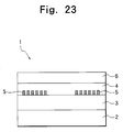
- Fig. 23 typically illustrate an example of a layer constitution of SAW device.
- propagation velocity V, effective coupling coefficient K 2 and temperature coefficient with frequency TCF have been improved, in particular by focusing first mode surface acoustic wave: for example, V of 8,000 to 10,000 (m/s), TCF of - 10 to 10 (ppm/°C) and K 2 of 0.7 to 1.7 (%) are achieved for the layer constitution of SiO 2 /ZnO/diamond shown in Fig. 23.
- the ZnO is piezoelectric material
- the SiO 2 is passivating layer for protecting both of the piezoelectric material and the IDT
- the IDT is formed of aluminum (Al), which is advantageous material in fabricating into desired dimension and shape.
- SiO 2 layer a temperature coefficient of which is inverse to that of ZnO, is formed to an appropriate thickness so that smaller temperature coefficient for frequency is achieved by compensating increase/decrease of temperature coefficient of ZnO with decrease/increase of that of SiO 2 , respectively.
- Such SAW devices can have much thinner Al IDT than ZnO and SiO 2 , when the device is operated at lower frequency on the order of several hundred MHz.
- SAW devices for 0th mode surface acoustic wave having V of 8,000 to 9,200 (m/s), TCF of -10 to 10 (ppm/°C), and lower propagation loss than that of SAW devices of aforementioned US Patent No. 5,446,329 to Nakahata et.al.
- SAW devices for 1st mode surface acoustic wave having V of 9,000 to 12,800 (m/s), TCF of -10 to 10 (ppm/°C), and lower propagation loss than that of SAW devices of aforementioned US Patent No. 5,446,329.
- the layer structure of this SAW device is schematically illustrated in Fig. 23, and the region A-B-C-D-E-F-A indicating the preferable combination of kh1 and kh2 is shown in a two-dimensional Cartesian coordinate graph of Fig. 3.
- the SAW device having above constitution is capable of being provided with propagation velocity V of from 8,000 to 9,200 (m/s) and temperature coefficient for frequency TCF of from -10 to 10 (ppm/°C).
- the SAW device is also capable of being provided with propagation loss of 0.03 (dB/ ⁇ ).
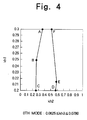
- the layer structure of this SAW device is schematically illustrated in Fig. 23, and the region A-B-C-D-E-F-A indicating the preferable combination of kh1 and kh2 is shown in a two-dimensional Cartesian coordinate graph of Fig. 4.
- the SAW device having above constitution is capable of being provided with propagation velocity V of from 8,000 to 9,200 (m/s) and temperature coefficient for frequency TCF of from -10 to 10 (ppm/°C).
- the SAW device is also capable of being provided with propagation loss of 0.03 (dB/ ⁇ ), which is lower than that of SAW devices (0.051 - 0.053 (db/ ⁇ )) of aforementioned US Patent No. 5,446,329.
- the layer structure of this SAW device is schematically illustrated in Fig. 23, and the region A-B-C-D-E-F-A indicating the preferable combination of kh1 and kh2 is shown in a two-dimensional Cartesian coordinate graph of Fig. 5.
- the SAW device having above constitution is capable of being provided with propagation velocity V of from 9,200 to 12,800 (m/s), the lower and higher limits of which are higher than that of SAW device for 1st mode SAW (V: 8,000 to 10,000) disclosed in aforementioned US Patent No. 5,446,329, and temperature coefficient for frequency TCF of from -10 to 10 (ppm/°C).
- the SAW device is also capable of being provided with propagation loss of 0.05 (dB/ ⁇ ).
- the layer structure of this SAW device is schematically illustrated in Fig. 23, and the region A-B-C-D-E-A indicating the preferable combination of kh1 and kh2 is shown in a two-dimensional Cartesian coordinate graph of Fig. 6.
- the SAW device having above constitution is capable of being provided with propagation velocity V of from 9,200 to 12,800 (m/s), the lower and higher limits of which are higher than that of SAW device for 1st mode SAW (V: 8,000 to 10,000) disclosed in aforementioned US Patent No. 5,446,329, and temperature coefficient for frequency TCF of from -10 to 10 (ppm/°C).
- the SAW device is also capable of being provided with propagation loss of 0.05 (dB/ ⁇ ), which is lower than that of SAW devices for 1st mode SAW (0.079 - 0.083 (db/ ⁇ )) of aforementioned US Patent No. 5,446,329.
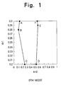
- the layer structure of this SAW device is schematically illustrated in Fig. 23, and the region A-B-C-D-E-F-A indicating the preferable combination of kh1 and kh2 is shown in a two-dimensional Cartesian coordinate graph of Fig. 1.
- the SAW device having above constitution is capable of being provided with propagation velocity V of from 8,000 to 9,200 (m/s), and temperature coefficient for frequency TCF of from -10 to 10 (ppm/°C).
- the SAW device is also capable of being provided with propagation loss of 0.03 (dB/ ⁇ ), which is lower than that of SAW devices for 0th mode SAW (0.051 - 0.053 (db/ ⁇ )) of aforementioned US Patent No. 5,446,329.
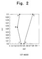
- the layer structure of this SAW device is schematically illustrated in Fig. 23, and the region A-B-C-D-E-A indicating the preferable combination of kh1 and kh2 is shown in a two-dimensional Cartesian coordinate graph of Fig. 2.
- the SAW device having above constitution is capable of being provided with propagation velocity V of from 9,000 to 12,800 (m/s), and temperature coefficient for frequency TCF of from -10 to 10 (ppm/°C).
- the SAW device is also capable of being provided with propagation loss of 0.05 (dB/ ⁇ ), which is lower than that of SAW devices for 1st mode SAW (0.079 - 0.083 (db/ ⁇ )) of aforementioned US Patent No. 5,446,329.
- Each of these six SAW devices (the first to the sixth SAW devices) according to the present invention has the SiO 2 layer of the appropriate thickness, so that the device is provided with higher effective coupling coefficient(K 2 ) for effectively converting the electrical energy into mechanical energy on the surface of the device.
- Fig. 23 is a schematic cross-sectional view of the SAW device according to the present invention.
- a SAW device 1 according to the present invention has an aluminum interdigital transducer (Al IDT) 5 formed on a surface of a diamond layer 3 deposited on a Si layer 2.
- Diamond layer 3 serves as a hard material layer for enhancing propagation velocity of surface acoustic device (SAW).
- IDTs 5 are formed at the input and the output sides, respectively.
- ZnO layer 4 the piezoelectric material layer, is formed so as to cover IDTs 5, and an amorphous SiO 2 layer 6 is formed so that ZnO layer 4 and IDTs 5 are protected by the passivating amorphous silicon layer 6.
- the diamond material preferable for the use in the present invention may be either natural diamond or synthetic diamond.
- the diamond may be single crystalline diamond or polycrystalline diamond.
- the diamond plate/substrate itself can be used for fabricating SAW devices according to the present invention.
- Diamond layer/film formed on the other base material can also be employed.
- the base material used for forming diamond film is not particularly limited, but may appropriately be selected depending on the usage of the SAW device.
- the base material to be available in the present invention may comprise semiconductor materials such as crystalline silicon, amorphus silicon, metals, glass and ceramics.
- the process may appropriately be selected from known synthesis processes such as CVD(Chemical Vapor Deposition) including microwave plasma CVD, plasma enhanced CVD, PVD(Physical Vapor Deposition), sputtering, ion plating, plasma jet method, flame method and hot filament method.
- the plane orientation of the diamond may be any of (111), (100) and (110), etc., or may be any combination of these plane orientations.
- ZnO layer that is disposed on the diamond and functions as piezoelectric layer of the SAW device according to the present invention, is preferably polycrystalline, and c-axis oriented, in view of piezoelectric property.
- c-axis oriented it is meant that ZnO layer have a (001) plane that is parallel to a base layer, such as diamond layer, on which the ZnO layer is disposed.
- SiO 2 layer that is formed on the ZnO layer and functions as protecting or passivating material for the ZnO layer and IDT according to the present invention, is preferably an amorphous SiO 2 layer, in view of electric and mechanical properties of the formed SAW device and formability and processibility.
- SiO 2 layer can compensate the variation of the SAW propagation velocity through diamond and ZnO layers to provide the operation stability for temperature variation.
- the planar or projected shape of the IDT for the SAW device of the present invention is not limited. Electrode called “single-type” electrode 8 as shown in the schematic plan view of Fig. 24A or electrode called “double-type” electrode 9 as shown in the schematic plan view of Fig. 24B may typically be used for the present invention.
- a pair of IDTs are disposed at input side and output side.
- Any of electric conductive materials can be used for interdigital transducer for the SAW device of the present invention.
- Al aluminum
- Al may preferably be used as the material for the IDT.
- the thickness of the IDT is not limited, as long as it functions as an IDT of a SAW device.
- the thickness of the IDT may typically be in the range of about 100 to about 5,000 ⁇ (more preferably, about 100 to 500 ⁇ ).
- the electrode resistivity is increased, causing considerable energy loss.
- the thickness of the IDT exceeds 5,000 ⁇ , considerable mass addition effect cause reflection of SAW, and desired SAW characteristic of the SAW device may suffer.
- the preferable ratio of ZnO piezoelectric layer thickness to Al IDT thickness: (t1/t3) may be 1.5 to 8.0, more preferably 2.0 to 7.0, most preferably 2.54 to 6.37, in view of properties such as durability and operating characteristics of the resulting SAW devices.
- the preferable range of the ratio of ZnO piezoelectric layer thickness to Al IDT thickness: (t1/t3) may be at least 10, in view of avoiding the effect of Al IDT to characteristics of SAW device.
- SAW devices having a layer constitution illustrated in Fig. 23, and also having different thicknesses of Al IDT 5, ZnO layer, and SiO 2 layer 6, were prepared, and the obtained SAW devices were evaluated on the propagation velocity V and the temperature coefficient for frequency TCF. Also, the SAW devices having different spacing between an input and an output IDTs were prepared so as to evaluate the relationship of the propagating length of SAW and the device insertion loss to give the propagation loss of the SAW device.
- SAW device 1 As shown Fig. 23, SAW device 1 according to the present invention is provided with IDT 5 formed on the surface of diamond layer 3 overlying an Si layer 2, and ZnO layer 4 is formed to cover IDT 5.
- SiO 2 layer 6 is formed on ZnO layer 4 to cover ZnO layer 4 and IDT 5 to form SAW device 1.
- IDTs 5 are made of aluminum (Al), and two pairs of IDT as the input and the output IDTs are formed.
- kh1 (2 ⁇ / ⁇ )t1
- kh2 (2 ⁇ / ⁇ )t2
- each of the SAW devices of two experimental groups has the same layer constitution as shown in Fig. 23 but different thickness of layers 4,6 and IDT 5, according to the present invention.
- the third experimental group of the SAW devices for the comparison which have the layer constitution shown in Fig. 23 but satisfying relationship of kh1 (kh of ZnO) and kh2 (kh of SiO 2 ) surrounded by 4 circles in Fig. 15 of US Patent No. 5,446,329, as described in "EMBODIMENT 6" (13th column, line 56 to 14th column, line 126) were also prepared.
- the thickness of Al IDT 5 of each devices in the series of SAW devices of the second experimental group also has a different thickness in 10 thickness ranging from 300 to 500 angstroms.
- SAW devices of the experimental groups 1, 2 and 3 were manufactured as follows.
- the Si substrate 2 having diamond layer 3 thereon was obtained.
- Al layer was deposited on diamond layer 3 via DC sputtering as follows.
- Substrate 2 was transferred to interior of a DC sputtering chamber, and Ar gas of sputtering gas was introduced into the chamber.
- DC power of 2.5 kW was applied under the ambient temperature, while the chamber pressure was maintained to be 10 mTorr, to deposit Al layer having the thickness of Al IDT on diamond layer 3 at a deposition rate of 50 (angstrom/sec.).
- the deposited Al layer was patterned via conventional photolithography and etching to obtain IDT 5 having the predetermined IDT pattern and dimensions. In this process, IDT was formed to have pad electrode portion.
- the substrate was transferred to a vacuum chamber of a magnetron sputtering apparatus to deposit ZnO layer.
- a polycrystalline ZnO target was included within the chamber.
- Portion of ZnO layer 4 and SiO 2 layer 6 overlying the pad electrode portion of IDT 5 was removed by conventional photolithography to expose Al of the pad portion. Thus, the manufacturing of the SAW device was completed.
- radio frequency (RF) power was applied to the input IDT to generate SAW of 0th and 1st modes.
- TCF measurement was carried out by the following manner: SAW device was heated by an external heater from room temperature to 70°C. The central frequency F 0 was measured at every 10°C from the room temperature to 70°C. Proportional relationship between the central frequency and the device temperature. TCF was given by the slope of the relationship.
- propagation loss was evaluated by the following manner: SAW devices having same layer/electrode constitution but different spacing between input IDT and output IDT (e.g., 50 wavelength, 100 wavelength and 150 wave length) were fabricated. A relationship of insertion loss with the spacing was evaluated and found that the insertion loss was proportional to the spacing. Then the propagation loss could be obtained by the slope of the relationship. These measurements were conducted by using a network analyzer ("Network Analyzer 8719A", commercially available from Yokogawa Hewlett Packard (YHP), Japan).
- the thickness t1 ( ⁇ m) of the ZnO layers of each SAW devices, and the thickness t2 ( ⁇ m) of the SiO 2 layers of each SAW device were measured by cutting off the device after the measurement of device performances as described above, and observing the resultant section of the device with a scanning electron microscope (SEM).
- SEM scanning electron microscope
- EXAMPLE 1-1 The first experimental group of SAW devices - (1): optimization of thickness relationship of SAW devices for 0th mode, the fifth SAW device according to the present invention.
- the thickness ratio of ZnO piezoelectric layer 4 (t1) to Al IDT 5 (t3) is: 12.7 ⁇ (t1/t3).
- Variation of the propagation velocity V and the temperature coefficient for frequency TCF, respectively, with the dimensionless thickness of ZnO layer and SiO 2 layer are illustrated in Figs. 7 and 8, respectively.
- Fig. 7 is a graph showing the variations of V when dimensionless thickness kh1 of ZnO layer and kh2 of SiO 2 layer vary.
- Fig. 8 is a graph showing the variations of TCF when dimensionless thickness kh1 of ZnO layer and kh2 of SiO 2 layer vary.
- dotted lines appearing the left most of the graph indicate the boundaries that the devices would not be form-able as a SAW device when the dimensionless thickness kh2 of SiO 2 layer decreases to a dimensionless thickness less than the boundaries.
- Example 1-1 have been described for the SAW devices having the thickness ratio (t1/t3) ⁇ 12.7, it is thought that the preferable range of kh1 and kh2 included in the region A-B-C-D-E-F-A shown in Fig. 1 is also applicable to the SAW devices having the thickness ratio (t1/t3) ⁇ 10, because the Al IDT of such devices having the thickness ratio (t1/t3) ⁇ 10 will not affect the characteristics of SAW devices.
- EXAMPLE 1-2 The first experimental group of SAW devices - (2): optimization of thickness relationship of SAW devices for 1st mode, the sixth SAW device according to the present invention.
- the thickness ratio of ZnO piezoelectric layer 4 (t1) to Al IDT 5 (t3) of the SAW devices of Example 1-2 is: 12.7 ⁇ (t1/t3).
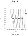
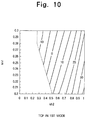
- Variation of the propagation velocity V and the temperature coefficient for frequency TCF, respectively, with the dimensionless thickness of ZnO layer and SiO 2 layer are illustrated in Figs. 9 and 10, respectively.
- Fig. 9 is a graph showing the variations of V when dimensionless thickness kh1 of ZnO layer and kh2 of SiO 2 layer vary.
- Fig. 10 is a graph showing the variations of TCF when dimensionless thickness kh1 of ZnO layer and kh2 of SiO 2 layer vary.
- dotted lines appearing the left most of the graph indicate the boundaries that the devices would not be form-able as a SAW device when the dimensionless thickness kh2 of SiO 2 layer decreases to a dimensionless thickness less than the boundaries.
- Example 1-2 have been described for the SAW devices having the thickness ratio (t1/t3) ⁇ 12.7, it is thought that the preferable range of kh1 and kh2 included in the region A-B-C-D-E-A shown in Fig. 2 is also applicable to the SAW devices having the thickness ratio (t1/t3) ⁇ 10, because the Al IDT of such devices having the thickness ratio (t1/t3) ⁇ 10 will not affect the characteristics of SAW devices.
- EXAMPLE 2-1 The second experimental group of SAW devices - (1): optimization of thickness relationship of SAW devices for 0th mode, the first and the second SAW devices according to the present invention.
- the thickness ratio of ZnO piezoelectric layer 4 (t1) to Al IDT 5 (t3) is: 2.54 ⁇ (t1/t3) ⁇ 6.37. It has been found that, in the devices having such thickness ratio (t1/t3), the thickness of the Al IDT is so large with reference to the thickness of ZnO layer that the characteristics such as V, TCF and the propagation loss of the SAW devices are affected by the thickness of the IDT.
- the SAW devices having different thickness of Al IDT 5, as well as different thickness of ZnO and SiO 2 layers were fabricated to determine optimal dimensionless thickness kh3 of Al IDT 5, as well as the dimensionless thickness kh1 and kh2.
- dotted lines appearing the left most of the graph indicate the boundaries of the kh2 that the devices would not be form-able as a SAW device when the dimensionless thickness kh2 of SiO 2 layer decreases to a dimensionless thickness less than the boundaries.
- the optimal kh1 and kh2 for providing the preferable V and TCF should be included in a region A-B-C-D-E-F-A shown in Fig. 3, to obtain the first SAW device of the present invention.
- the propagation loss of the first SAW devices was measured and the results were 0.026 to 0.032 (dB/ ⁇ ), as shown in TABLE -3.
- the propagation loss of the second SAW devices was measured and the results were 0.028 to 0.032 (dB/ ⁇ ), as shown in TABLE -4.
- EXAMPLE 2-2 The second experimental group of SAW devices - (2): optimization of thickness relationship of SAW devices for 1st mode, the third and the fourth SAW devices according to the present invention.
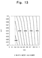
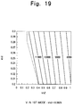
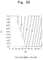
- Example 2-1 In the second experimental group of SAW devices for utilizing 1st mode SAW, the SAW devices having different thickness of Al IDT 5, as well as different thickness of ZnO and SiO 2 layers, were fabricated to determine optimal dimensionless thickness kh3 of Al IDT 5, as well as the dimensionless thickness kh1 and kh2, as conducted in Example 2-1. Similarly as in Example 2-1, optimal ranges of kh1 and kh2 in the case of SAW devices having kh3 of from 0.047 to 0.0780 were determined, for the second experimental group of SAW devices.
- this phenomenon can be applied to the shifting of the TCF-contours with the change of kh3, in which TCF-contours in Fig. 18 are monotonically and continuously shifted through corresponding one in Fig. 20 to corresponding one in Fig. 22, with the change of kh3 from 0.047 through 0.0625 to 0.0780.
- dotted lines appearing the left most of the graph indicate the boundaries of the kh2 that the devices would not be form-able as a SAW device when the dimensionless thickness kh2 of SiO 2 layer decreases to a dimensionless thickness less than the boundaries.
- the optimal kh1 and kh2 for providing the preferable V and TCF should be included in a region A-B-C-D-E-F-A shown in Fig. 5, to obtain the third SAW device of the present invention.
- the propagation loss of the third SAW devices was measured and the results were 0.047 to 0.053 (dB/ ⁇ ), as shown in TABLE -5.
- the propagation loss of the fourth SAW devices was measured and the results were 0.046 to 0.051 (dB/ ⁇ ), as shown in TABLE -6.
- COMPARATIVE EXAMPLE The third (comparative) experimental group of SAW devices: measurements of the propagation loss of the SAW device according to US Patent No. 5,446,329 to Nakahata et.al, for comparison with the SAW device of the present invention.
- propagation loss was also evaluated by the same manner as in Examples 1-1 to 2-2: SAW devices having same layer/electrode constitution but different spacing between input IDT and output IDT (e.g., 50 wavelength, 100 wavelength and 150 wave length) were fabricated. A relationship of insertion loss with the spacing was evaluated and found that the insertion loss was proportional to the spacing. Then the propagation loss could be obtained by the slope of the relationship.
- the obtained propagation losses in the comparative example were 0.051 to 0.053 (dB/ ⁇ ) for 0th mode SAW, as shown in TABLE - 7, which were higher than that of SAW devices according to the present invention shown in TABLES 1, 3 and 4. Also, for 1st mode SAW, the obtained propagation losses were 0.079 to 0.083 (dB/ ⁇ ), as shown in TABLE - 7, which were higher than that of SAW devices according to the present invention shown in TABLES 1, 3 and 4.
- the SAW devices according to the present invention have excellent propagation loss, as well as propagation velocity V and temperature coefficient TCF.
Landscapes
- Physics & Mathematics (AREA)
- Acoustics & Sound (AREA)
- Surface Acoustic Wave Elements And Circuit Networks Thereof (AREA)
Applications Claiming Priority (3)
| Application Number | Priority Date | Filing Date | Title |
|---|---|---|---|
| JP27626095 | 1995-09-29 | ||
| JP27626095A JP3205981B2 (ja) | 1995-09-29 | 1995-09-29 | 表面弾性波素子 |
| JP276260/95 | 1995-09-29 |
Publications (3)
| Publication Number | Publication Date |
|---|---|
| EP0766383A2 true EP0766383A2 (fr) | 1997-04-02 |
| EP0766383A3 EP0766383A3 (fr) | 1998-01-14 |
| EP0766383B1 EP0766383B1 (fr) | 2001-12-05 |
Family
ID=17566958
Family Applications (1)
| Application Number | Title | Priority Date | Filing Date |
|---|---|---|---|
| EP96115405A Expired - Lifetime EP0766383B1 (fr) | 1995-09-29 | 1996-09-25 | Dispositif à ondes acoustiques de surface à diamant-ZnO comportant une couche relativement mince de ZnO piézoélectrique |
Country Status (5)
| Country | Link |
|---|---|
| US (1) | US5777422A (fr) |
| EP (1) | EP0766383B1 (fr) |
| JP (1) | JP3205981B2 (fr) |
| CA (1) | CA2186185C (fr) |
| DE (1) | DE69617593T2 (fr) |
Cited By (3)
| Publication number | Priority date | Publication date | Assignee | Title |
|---|---|---|---|---|
| EP0841749A1 (fr) * | 1996-11-07 | 1998-05-13 | Sumitomo Electric Industries, Ltd. | Dispositif à ondes acoustiques de surface à diamant-ZnO |
| US5814918A (en) * | 1995-08-08 | 1998-09-29 | Sumitomo Electric Industries, Ltd. | Diamond-ZnO surface acoustic wave device |
| US5959389A (en) * | 1995-08-08 | 1999-09-28 | Sumitomo Electronic Industries, Ltd. | Diamond-ZnO surface acoustic wave device |
Families Citing this family (13)
| Publication number | Priority date | Publication date | Assignee | Title |
|---|---|---|---|---|
| US6713941B2 (en) | 2000-03-24 | 2004-03-30 | Seiko Epson Corporation | Surface acoustic wave element |
| JP2002057549A (ja) * | 2000-08-09 | 2002-02-22 | Sumitomo Electric Ind Ltd | 表面弾性波素子用基板及び表面弾性波素子 |
| US6930364B2 (en) * | 2001-09-13 | 2005-08-16 | Silicon Light Machines Corporation | Microelectronic mechanical system and methods |
| US6846423B1 (en) | 2002-08-28 | 2005-01-25 | Silicon Light Machines Corporation | Wafer-level seal for non-silicon-based devices |
| JP2005537661A (ja) * | 2002-08-28 | 2005-12-08 | シリコン・ライト・マシーンズ・コーポレーション | 非シリコン系素子のウエハー段階でのシール |
| US6877209B1 (en) * | 2002-08-28 | 2005-04-12 | Silicon Light Machines, Inc. | Method for sealing an active area of a surface acoustic wave device on a wafer |
| US20040091208A1 (en) * | 2002-11-12 | 2004-05-13 | Yutaka Doi | Planar optical wave-guide with dielectric mirrors |
| US7645513B2 (en) * | 2003-02-14 | 2010-01-12 | City University Of Hong Kong | Cubic boron nitride/diamond composite layers |
| WO2004095699A1 (fr) * | 2003-04-18 | 2004-11-04 | Murata Manufacturing Co., Ltd. | Dispositif a onde limite elastique |
| WO2005099088A1 (fr) * | 2004-03-26 | 2005-10-20 | Cypress Semiconductor Corp. | Circuit integre comprenant un ou plusieurs dispositifs conducteurs formes sur un dispositif saw et/ou mems |
| EP1926211A3 (fr) * | 2006-11-21 | 2013-08-14 | Imec | Résonateur à mode découpage en épaisseur à diamant amélioré |
| US7579759B2 (en) * | 2007-06-11 | 2009-08-25 | City University Of Hong Kong | Surface acoustic wave (SAW) devices based on cubic boron nitride/diamond composite structures |
| US9973169B2 (en) * | 2015-10-01 | 2018-05-15 | Qorvo Us, Inc. | Surface acoustic wave filter with a cap layer for improved reliability |
Family Cites Families (7)
| Publication number | Priority date | Publication date | Assignee | Title |
|---|---|---|---|---|
| US4952832A (en) * | 1989-10-24 | 1990-08-28 | Sumitomo Electric Industries, Ltd. | Surface acoustic wave device |
| JP2885349B2 (ja) * | 1989-12-26 | 1999-04-19 | 住友電気工業株式会社 | 表面弾性波素子 |
| EP0534354A1 (fr) * | 1991-09-25 | 1993-03-31 | Sumitomo Electric Industries, Limited | Procédé de fabrication de dispositif à ondes acoustiques de surface et son procédé de fabrication |
| JP3225495B2 (ja) * | 1992-02-21 | 2001-11-05 | 住友電気工業株式会社 | 表面弾性波素子及びその製造方法 |
| JP3205976B2 (ja) * | 1992-09-14 | 2001-09-04 | 住友電気工業株式会社 | 表面弾性波素子 |
| JP3163606B2 (ja) * | 1993-01-29 | 2001-05-08 | 住友電気工業株式会社 | 表面弾性波素子 |
| JP3344441B2 (ja) * | 1994-03-25 | 2002-11-11 | 住友電気工業株式会社 | 表面弾性波素子 |
-
1995
- 1995-09-29 JP JP27626095A patent/JP3205981B2/ja not_active Expired - Lifetime
-
1996
- 1996-09-23 CA CA002186185A patent/CA2186185C/fr not_active Expired - Lifetime
- 1996-09-25 EP EP96115405A patent/EP0766383B1/fr not_active Expired - Lifetime
- 1996-09-25 DE DE69617593T patent/DE69617593T2/de not_active Expired - Lifetime
- 1996-09-27 US US08/720,369 patent/US5777422A/en not_active Expired - Lifetime
Cited By (3)
| Publication number | Priority date | Publication date | Assignee | Title |
|---|---|---|---|---|
| US5814918A (en) * | 1995-08-08 | 1998-09-29 | Sumitomo Electric Industries, Ltd. | Diamond-ZnO surface acoustic wave device |
| US5959389A (en) * | 1995-08-08 | 1999-09-28 | Sumitomo Electronic Industries, Ltd. | Diamond-ZnO surface acoustic wave device |
| EP0841749A1 (fr) * | 1996-11-07 | 1998-05-13 | Sumitomo Electric Industries, Ltd. | Dispositif à ondes acoustiques de surface à diamant-ZnO |
Also Published As
| Publication number | Publication date |
|---|---|
| DE69617593T2 (de) | 2002-05-02 |
| CA2186185A1 (fr) | 1997-03-30 |
| US5777422A (en) | 1998-07-07 |
| DE69617593D1 (de) | 2002-01-17 |
| EP0766383B1 (fr) | 2001-12-05 |
| CA2186185C (fr) | 2006-08-01 |
| JP3205981B2 (ja) | 2001-09-04 |
| EP0766383A3 (fr) | 1998-01-14 |
| JPH0998059A (ja) | 1997-04-08 |
Similar Documents
| Publication | Publication Date | Title |
|---|---|---|
| EP0766383B1 (fr) | Dispositif à ondes acoustiques de surface à diamant-ZnO comportant une couche relativement mince de ZnO piézoélectrique | |
| EP0435189B1 (fr) | Dispositif à ondes acoustiques de surface | |
| EP0588261B1 (fr) | Elément à ondes acoustiques de surface | |
| EP0674385B1 (fr) | Matériau orientable, substrat orientable et dispositif à ondes acoustiques de surface | |
| EP0688098B1 (fr) | Dispositif à onde acoustique de surface en diamant-LiTaO3 | |
| US5838090A (en) | Surface acoustic wave device | |
| JP3318920B2 (ja) | 表面弾性波素子 | |
| EP1309085A1 (fr) | Dispositif a onde acoustique de surface et son substrat | |
| US5814918A (en) | Diamond-ZnO surface acoustic wave device | |
| US6469416B1 (en) | Surface acoustic wave device | |
| US5959389A (en) | Diamond-ZnO surface acoustic wave device | |
| US5783896A (en) | Diamond-Zn0 surface acoustic wave device | |
| US6713941B2 (en) | Surface acoustic wave element | |
| JP3341759B2 (ja) | 表面弾性波素子 | |
| EP1225693A1 (fr) | Dispositif saw | |
| JP3365505B2 (ja) | 表面弾性波素子 | |
| JP3365506B2 (ja) | 表面弾性波素子 | |
| EP0841749A1 (fr) | Dispositif à ondes acoustiques de surface à diamant-ZnO |
Legal Events
| Date | Code | Title | Description |
|---|---|---|---|
| PUAI | Public reference made under article 153(3) epc to a published international application that has entered the european phase |
Free format text: ORIGINAL CODE: 0009012 |
|
| AK | Designated contracting states |
Kind code of ref document: A2 Designated state(s): DE FR GB NL |
|
| PUAL | Search report despatched |
Free format text: ORIGINAL CODE: 0009013 |
|
| AK | Designated contracting states |
Kind code of ref document: A3 Designated state(s): DE FR GB NL |
|
| 17P | Request for examination filed |
Effective date: 19980219 |
|
| GRAG | Despatch of communication of intention to grant |
Free format text: ORIGINAL CODE: EPIDOS AGRA |
|
| 17Q | First examination report despatched |
Effective date: 20001220 |
|
| GRAG | Despatch of communication of intention to grant |
Free format text: ORIGINAL CODE: EPIDOS AGRA |
|
| GRAH | Despatch of communication of intention to grant a patent |
Free format text: ORIGINAL CODE: EPIDOS IGRA |
|
| GRAH | Despatch of communication of intention to grant a patent |
Free format text: ORIGINAL CODE: EPIDOS IGRA |
|
| GRAA | (expected) grant |
Free format text: ORIGINAL CODE: 0009210 |
|
| AK | Designated contracting states |
Kind code of ref document: B1 Designated state(s): DE FR GB NL |
|
| REG | Reference to a national code |
Ref country code: GB Ref legal event code: IF02 |
|
| REF | Corresponds to: |
Ref document number: 69617593 Country of ref document: DE Date of ref document: 20020117 |
|
| ET | Fr: translation filed | ||
| PLBE | No opposition filed within time limit |
Free format text: ORIGINAL CODE: 0009261 |
|
| STAA | Information on the status of an ep patent application or granted ep patent |
Free format text: STATUS: NO OPPOSITION FILED WITHIN TIME LIMIT |
|
| 26N | No opposition filed | ||
| REG | Reference to a national code |
Ref country code: GB Ref legal event code: 732E |
|
| NLS | Nl: assignments of ep-patents |
Owner name: SEIKO EPSON CORPORATION |
|
| REG | Reference to a national code |
Ref country code: FR Ref legal event code: TP |
|
| REG | Reference to a national code |
Ref country code: FR Ref legal event code: PLFP Year of fee payment: 20 |
|
| PGFP | Annual fee paid to national office [announced via postgrant information from national office to epo] |
Ref country code: NL Payment date: 20150809 Year of fee payment: 20 |
|
| PGFP | Annual fee paid to national office [announced via postgrant information from national office to epo] |
Ref country code: DE Payment date: 20150922 Year of fee payment: 20 Ref country code: GB Payment date: 20150923 Year of fee payment: 20 |
|
| PGFP | Annual fee paid to national office [announced via postgrant information from national office to epo] |
Ref country code: FR Payment date: 20150811 Year of fee payment: 20 |
|
| REG | Reference to a national code |
Ref country code: DE Ref legal event code: R071 Ref document number: 69617593 Country of ref document: DE |
|
| REG | Reference to a national code |
Ref country code: NL Ref legal event code: MK Effective date: 20160924 |
|
| REG | Reference to a national code |
Ref country code: GB Ref legal event code: PE20 Expiry date: 20160924 |
|
| PG25 | Lapsed in a contracting state [announced via postgrant information from national office to epo] |
Ref country code: GB Free format text: LAPSE BECAUSE OF EXPIRATION OF PROTECTION Effective date: 20160924 |