EP0766908B1 - Procede et dispositif permettant de recouvrir des cartes de circuits, notamment pour produire des modules multipuces - Google Patents
Procede et dispositif permettant de recouvrir des cartes de circuits, notamment pour produire des modules multipuces Download PDFInfo
- Publication number
- EP0766908B1 EP0766908B1 EP95923327A EP95923327A EP0766908B1 EP 0766908 B1 EP0766908 B1 EP 0766908B1 EP 95923327 A EP95923327 A EP 95923327A EP 95923327 A EP95923327 A EP 95923327A EP 0766908 B1 EP0766908 B1 EP 0766908B1
- Authority
- EP
- European Patent Office
- Prior art keywords
- coating
- printed circuit
- copper
- radiation
- thickness
- Prior art date
- Legal status (The legal status is an assumption and is not a legal conclusion. Google has not performed a legal analysis and makes no representation as to the accuracy of the status listed.)
- Expired - Lifetime
Links
Images


Classifications
-
- G—PHYSICS
- G03—PHOTOGRAPHY; CINEMATOGRAPHY; ANALOGOUS TECHNIQUES USING WAVES OTHER THAN OPTICAL WAVES; ELECTROGRAPHY; HOLOGRAPHY
- G03F—PHOTOMECHANICAL PRODUCTION OF TEXTURED OR PATTERNED SURFACES, e.g. FOR PRINTING, FOR PROCESSING OF SEMICONDUCTOR DEVICES; MATERIALS THEREFOR; ORIGINALS THEREFOR; APPARATUS SPECIALLY ADAPTED THEREFOR
- G03F7/00—Photomechanical, e.g. photolithographic, production of textured or patterned surfaces, e.g. printing surfaces; Materials therefor, e.g. comprising photoresists; Apparatus specially adapted therefor
- G03F7/16—Coating processes; Apparatus therefor
- G03F7/168—Finishing the coated layer, e.g. drying, baking, soaking
-
- B—PERFORMING OPERATIONS; TRANSPORTING
- B05—SPRAYING OR ATOMISING IN GENERAL; APPLYING FLUENT MATERIALS TO SURFACES, IN GENERAL
- B05C—APPARATUS FOR APPLYING FLUENT MATERIALS TO SURFACES, IN GENERAL
- B05C1/00—Apparatus in which liquid or other fluent material is applied to the surface of the work by contact with a member carrying the liquid or other fluent material, e.g. a porous member loaded with a liquid to be applied as a coating
- B05C1/006—Apparatus in which liquid or other fluent material is applied to the surface of the work by contact with a member carrying the liquid or other fluent material, e.g. a porous member loaded with a liquid to be applied as a coating for applying liquid or other fluent material to the edges of essentially flat articles
-
- B—PERFORMING OPERATIONS; TRANSPORTING
- B05—SPRAYING OR ATOMISING IN GENERAL; APPLYING FLUENT MATERIALS TO SURFACES, IN GENERAL
- B05C—APPARATUS FOR APPLYING FLUENT MATERIALS TO SURFACES, IN GENERAL
- B05C1/00—Apparatus in which liquid or other fluent material is applied to the surface of the work by contact with a member carrying the liquid or other fluent material, e.g. a porous member loaded with a liquid to be applied as a coating
- B05C1/04—Apparatus in which liquid or other fluent material is applied to the surface of the work by contact with a member carrying the liquid or other fluent material, e.g. a porous member loaded with a liquid to be applied as a coating for applying liquid or other fluent material to work of indefinite length
- B05C1/08—Apparatus in which liquid or other fluent material is applied to the surface of the work by contact with a member carrying the liquid or other fluent material, e.g. a porous member loaded with a liquid to be applied as a coating for applying liquid or other fluent material to work of indefinite length using a roller or other rotating member which contacts the work along a generating line
- B05C1/0808—Details thereof, e.g. surface characteristics
-
- G—PHYSICS
- G03—PHOTOGRAPHY; CINEMATOGRAPHY; ANALOGOUS TECHNIQUES USING WAVES OTHER THAN OPTICAL WAVES; ELECTROGRAPHY; HOLOGRAPHY
- G03F—PHOTOMECHANICAL PRODUCTION OF TEXTURED OR PATTERNED SURFACES, e.g. FOR PRINTING, FOR PROCESSING OF SEMICONDUCTOR DEVICES; MATERIALS THEREFOR; ORIGINALS THEREFOR; APPARATUS SPECIALLY ADAPTED THEREFOR
- G03F7/00—Photomechanical, e.g. photolithographic, production of textured or patterned surfaces, e.g. printing surfaces; Materials therefor, e.g. comprising photoresists; Apparatus specially adapted therefor
- G03F7/16—Coating processes; Apparatus therefor
-
- H—ELECTRICITY
- H05—ELECTRIC TECHNIQUES NOT OTHERWISE PROVIDED FOR
- H05K—PRINTED CIRCUITS; CASINGS OR CONSTRUCTIONAL DETAILS OF ELECTRIC APPARATUS; MANUFACTURE OF ASSEMBLAGES OF ELECTRICAL COMPONENTS
- H05K3/00—Apparatus or processes for manufacturing printed circuits
- H05K3/0091—Apparatus for coating printed circuits using liquid non-metallic coating compositions
-
- H—ELECTRICITY
- H05—ELECTRIC TECHNIQUES NOT OTHERWISE PROVIDED FOR
- H05K—PRINTED CIRCUITS; CASINGS OR CONSTRUCTIONAL DETAILS OF ELECTRIC APPARATUS; MANUFACTURE OF ASSEMBLAGES OF ELECTRICAL COMPONENTS
- H05K3/00—Apparatus or processes for manufacturing printed circuits
- H05K3/46—Manufacturing multilayer circuits
- H05K3/4644—Manufacturing multilayer circuits by building the multilayer layer by layer, i.e. build-up multilayer circuits
- H05K3/4661—Adding a circuit layer by direct wet plating, e.g. electroless plating; insulating materials adapted therefor
-
- H—ELECTRICITY
- H10—SEMICONDUCTOR DEVICES; ELECTRIC SOLID-STATE DEVICES NOT OTHERWISE PROVIDED FOR
- H10W—GENERIC PACKAGES, INTERCONNECTIONS, CONNECTORS OR OTHER CONSTRUCTIONAL DETAILS OF DEVICES COVERED BY CLASS H10
- H10W70/00—Package substrates; Interposers; Redistribution layers [RDL]
- H10W70/01—Manufacture or treatment
- H10W70/05—Manufacture or treatment of insulating or insulated package substrates, or of interposers, or of redistribution layers
-
- H—ELECTRICITY
- H05—ELECTRIC TECHNIQUES NOT OTHERWISE PROVIDED FOR
- H05K—PRINTED CIRCUITS; CASINGS OR CONSTRUCTIONAL DETAILS OF ELECTRIC APPARATUS; MANUFACTURE OF ASSEMBLAGES OF ELECTRICAL COMPONENTS
- H05K2201/00—Indexing scheme relating to printed circuits covered by H05K1/00
- H05K2201/02—Fillers; Particles; Fibers; Reinforcement materials
- H05K2201/0203—Fillers and particles
- H05K2201/0206—Materials
- H05K2201/0209—Inorganic, non-metallic particles
-
- H—ELECTRICITY
- H05—ELECTRIC TECHNIQUES NOT OTHERWISE PROVIDED FOR
- H05K—PRINTED CIRCUITS; CASINGS OR CONSTRUCTIONAL DETAILS OF ELECTRIC APPARATUS; MANUFACTURE OF ASSEMBLAGES OF ELECTRICAL COMPONENTS
- H05K2203/00—Indexing scheme relating to apparatus or processes for manufacturing printed circuits covered by H05K3/00
- H05K2203/01—Tools for processing; Objects used during processing
- H05K2203/0104—Tools for processing; Objects used during processing for patterning or coating
- H05K2203/0143—Using a roller; Specific shape thereof; Providing locally adhesive portions thereon
-
- H—ELECTRICITY
- H05—ELECTRIC TECHNIQUES NOT OTHERWISE PROVIDED FOR
- H05K—PRINTED CIRCUITS; CASINGS OR CONSTRUCTIONAL DETAILS OF ELECTRIC APPARATUS; MANUFACTURE OF ASSEMBLAGES OF ELECTRICAL COMPONENTS
- H05K2203/00—Indexing scheme relating to apparatus or processes for manufacturing printed circuits covered by H05K3/00
- H05K2203/07—Treatments involving liquids, e.g. plating, rinsing
- H05K2203/0756—Uses of liquids, e.g. rinsing, coating, dissolving
- H05K2203/0773—Dissolving the filler without dissolving the matrix material; Dissolving the matrix material without dissolving the filler
-
- H—ELECTRICITY
- H05—ELECTRIC TECHNIQUES NOT OTHERWISE PROVIDED FOR
- H05K—PRINTED CIRCUITS; CASINGS OR CONSTRUCTIONAL DETAILS OF ELECTRIC APPARATUS; MANUFACTURE OF ASSEMBLAGES OF ELECTRICAL COMPONENTS
- H05K2203/00—Indexing scheme relating to apparatus or processes for manufacturing printed circuits covered by H05K3/00
- H05K2203/07—Treatments involving liquids, e.g. plating, rinsing
- H05K2203/0779—Treatments involving liquids, e.g. plating, rinsing characterised by the specific liquids involved
- H05K2203/0786—Using an aqueous solution, e.g. for cleaning or during drilling of holes
- H05K2203/0789—Aqueous acid solution, e.g. for cleaning or etching
-
- H—ELECTRICITY
- H05—ELECTRIC TECHNIQUES NOT OTHERWISE PROVIDED FOR
- H05K—PRINTED CIRCUITS; CASINGS OR CONSTRUCTIONAL DETAILS OF ELECTRIC APPARATUS; MANUFACTURE OF ASSEMBLAGES OF ELECTRICAL COMPONENTS
- H05K2203/00—Indexing scheme relating to apparatus or processes for manufacturing printed circuits covered by H05K3/00
- H05K2203/08—Treatments involving gases
- H05K2203/081—Blowing of gas, e.g. for cooling or for providing heat during solder reflowing
-
- H—ELECTRICITY
- H05—ELECTRIC TECHNIQUES NOT OTHERWISE PROVIDED FOR
- H05K—PRINTED CIRCUITS; CASINGS OR CONSTRUCTIONAL DETAILS OF ELECTRIC APPARATUS; MANUFACTURE OF ASSEMBLAGES OF ELECTRICAL COMPONENTS
- H05K2203/00—Indexing scheme relating to apparatus or processes for manufacturing printed circuits covered by H05K3/00
- H05K2203/11—Treatments characterised by their effect, e.g. heating, cooling, roughening
- H05K2203/1105—Heating or thermal processing not related to soldering, firing, curing or laminating, e.g. for shaping the substrate or during finish plating
-
- H—ELECTRICITY
- H05—ELECTRIC TECHNIQUES NOT OTHERWISE PROVIDED FOR
- H05K—PRINTED CIRCUITS; CASINGS OR CONSTRUCTIONAL DETAILS OF ELECTRIC APPARATUS; MANUFACTURE OF ASSEMBLAGES OF ELECTRICAL COMPONENTS
- H05K2203/00—Indexing scheme relating to apparatus or processes for manufacturing printed circuits covered by H05K3/00
- H05K2203/11—Treatments characterised by their effect, e.g. heating, cooling, roughening
- H05K2203/1121—Cooling, e.g. specific areas of a PCB being cooled during reflow soldering
-
- H—ELECTRICITY
- H05—ELECTRIC TECHNIQUES NOT OTHERWISE PROVIDED FOR
- H05K—PRINTED CIRCUITS; CASINGS OR CONSTRUCTIONAL DETAILS OF ELECTRIC APPARATUS; MANUFACTURE OF ASSEMBLAGES OF ELECTRICAL COMPONENTS
- H05K2203/00—Indexing scheme relating to apparatus or processes for manufacturing printed circuits covered by H05K3/00
- H05K2203/15—Position of the PCB during processing
- H05K2203/1509—Horizontally held PCB
-
- H—ELECTRICITY
- H05—ELECTRIC TECHNIQUES NOT OTHERWISE PROVIDED FOR
- H05K—PRINTED CIRCUITS; CASINGS OR CONSTRUCTIONAL DETAILS OF ELECTRIC APPARATUS; MANUFACTURE OF ASSEMBLAGES OF ELECTRICAL COMPONENTS
- H05K2203/00—Indexing scheme relating to apparatus or processes for manufacturing printed circuits covered by H05K3/00
- H05K2203/15—Position of the PCB during processing
- H05K2203/1572—Processing both sides of a PCB by the same process; Providing a similar arrangement of components on both sides; Making interlayer connections from two sides
-
- H—ELECTRICITY
- H05—ELECTRIC TECHNIQUES NOT OTHERWISE PROVIDED FOR
- H05K—PRINTED CIRCUITS; CASINGS OR CONSTRUCTIONAL DETAILS OF ELECTRIC APPARATUS; MANUFACTURE OF ASSEMBLAGES OF ELECTRICAL COMPONENTS
- H05K3/00—Apparatus or processes for manufacturing printed circuits
- H05K3/0011—Working of insulating substrates or insulating layers
- H05K3/0017—Etching of the substrate by chemical or physical means
- H05K3/0023—Etching of the substrate by chemical or physical means by exposure and development of a photosensitive insulating layer
-
- H—ELECTRICITY
- H05—ELECTRIC TECHNIQUES NOT OTHERWISE PROVIDED FOR
- H05K—PRINTED CIRCUITS; CASINGS OR CONSTRUCTIONAL DETAILS OF ELECTRIC APPARATUS; MANUFACTURE OF ASSEMBLAGES OF ELECTRICAL COMPONENTS
- H05K3/00—Apparatus or processes for manufacturing printed circuits
- H05K3/10—Apparatus or processes for manufacturing printed circuits in which conductive material is applied to the insulating support in such a manner as to form the desired conductive pattern
- H05K3/108—Apparatus or processes for manufacturing printed circuits in which conductive material is applied to the insulating support in such a manner as to form the desired conductive pattern by semi-additive methods; masks therefor
-
- H—ELECTRICITY
- H05—ELECTRIC TECHNIQUES NOT OTHERWISE PROVIDED FOR
- H05K—PRINTED CIRCUITS; CASINGS OR CONSTRUCTIONAL DETAILS OF ELECTRIC APPARATUS; MANUFACTURE OF ASSEMBLAGES OF ELECTRICAL COMPONENTS
- H05K3/00—Apparatus or processes for manufacturing printed circuits
- H05K3/10—Apparatus or processes for manufacturing printed circuits in which conductive material is applied to the insulating support in such a manner as to form the desired conductive pattern
- H05K3/18—Apparatus or processes for manufacturing printed circuits in which conductive material is applied to the insulating support in such a manner as to form the desired conductive pattern using precipitation techniques to apply the conductive material
- H05K3/181—Apparatus or processes for manufacturing printed circuits in which conductive material is applied to the insulating support in such a manner as to form the desired conductive pattern using precipitation techniques to apply the conductive material by electroless plating
-
- H—ELECTRICITY
- H05—ELECTRIC TECHNIQUES NOT OTHERWISE PROVIDED FOR
- H05K—PRINTED CIRCUITS; CASINGS OR CONSTRUCTIONAL DETAILS OF ELECTRIC APPARATUS; MANUFACTURE OF ASSEMBLAGES OF ELECTRICAL COMPONENTS
- H05K3/00—Apparatus or processes for manufacturing printed circuits
- H05K3/22—Secondary treatment of printed circuits
- H05K3/227—Drying of printed circuits
Definitions
- the invention relates to a method for coating printed circuit boards with a coating agent which can be crosslinked by electromagnetic, preferably UV radiation according to the preamble of claim 1.
- the invention also relates to a suitable device according to the preamble of claim 6.
- Component A Resin (A - 3) 50 parts by weight 70% in cellosolve acetate Trimethylolpropane triacrylate 4 parts by weight Pentaerythritol triacrylate 4 parts by weight 2-ethylanthraquinone 3 parts by weight 2-phenyl-4-benzyl-5hydroxy-methylimidazo 10.5 parts by weight "AC - 300" 1.0 part by weight Phthalocyanine green 0.5 part by weight Calcium carbonate 10 parts by weight 75 parts by weight 80% by weight Component B "Epiclon EXA 1514" to phenol-s type epoxy resin from Dai-Nippon Ink & Chemical 10 parts by weight Trimethylolpropane triglycidyl ether 4 parts by weight Cellosolve acetate 6 parts by weight Calcium carbonate 5 parts by weight 25 parts by weight 80% by weight
Landscapes
- Engineering & Computer Science (AREA)
- Manufacturing & Machinery (AREA)
- Microelectronics & Electronic Packaging (AREA)
- Physics & Mathematics (AREA)
- General Physics & Mathematics (AREA)
- Non-Metallic Protective Coatings For Printed Circuits (AREA)
- Manufacturing Of Printed Circuit Boards (AREA)
- Application Of Or Painting With Fluid Materials (AREA)
Claims (10)
- Procédé permettant de recouvrir des cartes à circuits imprimés d'une couche réticulable par rayonnement ultraviolet selon un procédé de recouvrement au rouleau sur les deux faces, caractérisé en ce que les cartes à circuits imprimés (11) sont maintenues à température ambiante sur la face de la couche puis recouvertes d'un agent de recouvrement photopolymérisable, lequel possède une teneur en solides comprise entre 70 et 95 % en masse et une viscosité comprise entre 10 et 60 Pa.s à 25 °C, de façon telle que l'agent de recouvrement soit maintenu dans une zone de viscosité comprise entre 1 et 10 Pa.s au moyen de rouleaux doseurs (2) régulés entre 25 et 60 °C, appliqué sur la surface des cartes à circuits imprimés en couches d'une épaisseur comprise entre 10 et 200 µm au moyen de rouleaux d'application (1) polis et gommés, exempts d'agent de recouvrement sur les bords, et refroidis pour présenter une température de surface comprise entre 5 et 20 °C, avec une viscosité d'application comprise entre 20 et 100 Pa.s et une vitesse de recouvrement comprise entre 5 et 20 m/min., puis qu'il soit séché en 60 à 120 s à une température comprise entre 80 et 120 °C.
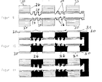
- Procédé selon la revendication 1, caractérisé en ce que, pour produire des modules multipuces, les cartes à circuits imprimés (11) sont recouvertes d'agents de recouvrement (13) réticulables par rayonnement sur des épaisseurs comprises entre 50 et 100µm, puis séchées, en ce que se forment, par exposition à un rayonnement ultraviolet en utilisant un masque perforé présentant des diamètres de trous de 50µm et développement des zones perforées non réticulées (14), des micro-perforations (16) qui après attaque à l'acide sont chimiquement cuivrées sur 1 µm avec la surface, et en ce que, après une seconde application d'un agent de recouvrement réticulable par rayonnement sur une épaisseur de couche comprise entre 10 et 20 µm, après séchage, photostructuration, développement, cuivrage par électrolyse sur 10 à 20 µm (17), décapage de l'agent de recouvrement et gravure différentielle de la couche de cuivre de 1 µm (15), des connexions de circuits imprimés de 100 à 200 µm de large sont produites par dessus les micro-perforations (16).
- Procédé selon la revendication 1, caractérisé en ce qu'il est possible d'obtenir, avec une application dans l'épaisseur de la hauteur du conducteur, un recouvrement du conducteur représentant 50 % et un recouvrement des arêtes du conducteur représentant 25 % de l'épaisseur de couche.
- Procédé selon la revendication 2, caractérisé en ce que l'agent de recouvrement contient un matériau de charge soluble dans l'acide et ininflammable, de préférence de l'hydroxyde de magnésium, présentant une taille de grain comprise entre 3 et 10µm, dans une quantité comprise entre 10 et 60 parties en masse.
- Procédé selon la revendication 2, caractérisé en ce que, pour produire une couche passivante de conducteur pour conducteurs en cuivre déposés chimiquement, avant le cuivrage chimique, la couche passivante de conducteur est photostructurée par rayonnement ultraviolet de façon telle que, après le développement des zones non réticulées entre les zones perforées réticulées (28), qui se présentent en forme de colonnes, se forment des empreintes (29) en forme de cavités, dans lesquelles le cuivre déposé chimiquement peut s'ancrer par adhésion.
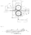
- Dispositif pour recouvrir les deux faces des cartes à circuits imprimés d'agents de recouvrement très visqueux et réticulables par rayonnement en utilisant un dispositif de recouvrement au rouleau double face, caractérisé en ce que le dispositif de recouvrement au rouleau présente deux rouleaux doseurs (2) pouvant être chauffés entre 25 et 60 °C et deux rouleaux d'application (1) gommés, pourvus d'un dispositif racleur de bords, polis et pouvant être refroidis à une température comprise entre 5 et 20 °C.
- Dispositif selon la revendication 6, caractérisé en ce que, pour produire un bord de substrat exempt d'agent de recouvrement, sont disposés respectivement contre chaque rouleau d'application refroidi (1), dans la zone des bords, deux racles tournantes chromées (4) pouvant être chauffées entre 60 et 90 °C se composant de préférence de rouleaux métalliques chauffés électriquement et présentant un diamètre compris de préférence entre 10 et 50 mm, et en ce que, contre les racles tournantes peuvent s'appuyer des racles à couteau (6) en tant qu'organes racleurs.
- Dispositif selon la revendication 6, caractérisé en ce que, pour que les cartes à circuits soient exemptes d'agent de recouvrement sur les bords, les rouleaux doseurs (2) présentant un diamètre de préférence égal à 150 mm présentent dans la zone des bords une couche d'écartement métallique (34) composée de préférence de chrome, appliquée par dépôt électrolytique et présentant une largeur comprise entre 10 et 100 mm et une épaisseur comprise entre 10 et 200 µm, et en ce que, dans la zone des bords des rouleaux d'application gommés et refroidis (1) présentant de préférence un diamètre de 200 mm, est disposée une bague à contact glissant (36) dans l'épaisseur du gommage, laquelle se compose d'un matériau synthétique conducteur, de préférence d'un stratifié, dans les couches de laquelle sont imprimées des feuilles de cuivre présentant une épaisseur comprise entre 35 et 500 mm, et par l'intermédiaire de laquelle le contact électrique avec la couche d'écartement métallique (34) de même largeur entre 2 et 20 mm peut être réalisé et l'épaisseur de la couche de recouvrement ajustée.
- Dispositif selon la revendication 6, caractérisé en ce que, pour recouvrir des surfaces de substrat profilées, le gommage des rouleaux d'application (1) possède une épaisseur comprise entre 10 et 20 mm et une dureté Shore comprise entre 40 et 60, dureté A, avec des rainures diagonales ou oscillantes d'une largeur et d'une profondeur préférées comprises entre 100 et 500 µm, et en ce que les rainures sont comblées avec un gommage présentant une dureté Shore comprise entre 10 et 20, puis polies.
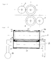
- Dispositif selon l'une des revendications 6 à 9, caractérisé en ce qu'en aval du dispositif de recouvrement au rouleau est disposé un séchoir laminaire à rayonnement et à convection, qui est équipé d'un canal de séchage horizontal (40) de 20 à 150 mm de haut et de 300 à 700 mm de large, et de préférence d'une longueur comprise entre 3 et 10 m, lequel est équipé en son milieu, pour le transport des cartes à circuits imprimés (9), de doubles bandes transporteuses avec guidage à rouleaux, réglables en largeur et pourvues d'un bain de rinçage (12), dans lequel est insufflé de l'air au niveau de la sortie du canal et à contre-courant par rapport à la direction du transport, par le biais d'une filière plate (41) amenée au-dessus et en-dessous du dispositif de transport respectivement, avec des vitesses d'écoulement indépendamment réglables et comprises entre 5 et 40 m/s, le canal de séchage (40) étant recouvert sur ses faces supérieure et inférieure de vitres (41), au-dessus et en-dessous desquelles, selon un écart de 20 à 200 mm, sont disposés de façon à pouvoir se déplacer horizontalement et verticalement des radiateurs aux rayons infrarouges (42) de longueur d'onde comprise entre 1 et 10 µm de sorte que le profil de température peut être réglé de façon individuelle en fonction des épaisseurs des cartes à circuits imprimés et des couches de laque.
Applications Claiming Priority (15)
| Application Number | Priority Date | Filing Date | Title |
|---|---|---|---|
| DE4421966 | 1994-06-23 | ||
| DE4421966 | 1994-06-23 | ||
| DE4428713 | 1994-08-12 | ||
| DE4428713 | 1994-08-12 | ||
| DE4434218 | 1994-09-26 | ||
| DE4434218 | 1994-09-26 | ||
| DE4444086 | 1994-12-12 | ||
| DE4444086 | 1994-12-12 | ||
| DE19500021 | 1995-01-03 | ||
| DE19500021 | 1995-01-03 | ||
| DE19510227 | 1995-03-23 | ||
| DE1995110227 DE19510227A1 (de) | 1995-03-23 | 1995-03-23 | Vorrichtung zur Einstellung gleichmäßiger Schichtstärken im Walzenauftrag |
| DE19516193A DE19516193A1 (de) | 1994-05-13 | 1995-05-08 | Verfahren und Vorrichtung zum Beschichten von Leiterplatten, insbesondere zur Herstellung von Multi-Chip-Modulen |
| DE19516193 | 1995-05-08 | ||
| PCT/EP1995/002309 WO1996000492A1 (fr) | 1994-06-23 | 1995-06-14 | Procede et dispositif permettant de recouvrir des cartes de circuits, notamment pour produire des modules multipuces |
Publications (2)
| Publication Number | Publication Date |
|---|---|
| EP0766908A1 EP0766908A1 (fr) | 1997-04-09 |
| EP0766908B1 true EP0766908B1 (fr) | 1998-12-16 |
Family
ID=27561597
Family Applications (1)
| Application Number | Title | Priority Date | Filing Date |
|---|---|---|---|
| EP95923327A Expired - Lifetime EP0766908B1 (fr) | 1994-06-23 | 1995-06-14 | Procede et dispositif permettant de recouvrir des cartes de circuits, notamment pour produire des modules multipuces |
Country Status (5)
| Country | Link |
|---|---|
| US (1) | US5804256A (fr) |
| EP (1) | EP0766908B1 (fr) |
| AT (1) | ATE174750T1 (fr) |
| AU (1) | AU2792395A (fr) |
| WO (1) | WO1996000492A1 (fr) |
Families Citing this family (13)
| Publication number | Priority date | Publication date | Assignee | Title |
|---|---|---|---|---|
| US6305769B1 (en) * | 1995-09-27 | 2001-10-23 | 3D Systems, Inc. | Selective deposition modeling system and method |
| US7669547B2 (en) * | 2001-03-14 | 2010-03-02 | 3M Innovative Properties Company | Coating apparatus |
| TWI290016B (en) * | 2002-10-14 | 2007-11-11 | Atotech Deutschland Gmbh | A process and an apparatus for coating printed circuit boards with laser-structurable, thermally curable solder stop lacquers and electroresists |
| CN100525586C (zh) * | 2002-10-14 | 2009-08-05 | 阿托特希德国有限公司 | 利用可用激光形成结构的、可热固化的焊料阻挡漆和不导电物对印刷电路板进行涂覆的方法和装置 |
| CN100573318C (zh) * | 2003-09-17 | 2009-12-23 | 富士胶片株式会社 | 光敏平版印刷版及其制备方法 |
| US7595092B2 (en) * | 2006-03-01 | 2009-09-29 | Pyrotite Coating Of Canada, Inc. | System and method for coating a fire-resistant material on a substrate |
| US20090163115A1 (en) * | 2007-12-20 | 2009-06-25 | Spirit Aerosystems, Inc. | Method of making acoustic holes using uv curing masking material |
| US8728950B2 (en) * | 2009-06-18 | 2014-05-20 | Konica Minolta Holdings, Inc. | Coating method, and organic electroluminescence element |
| US8557099B2 (en) * | 2010-10-25 | 2013-10-15 | Ppg Industries Ohio, Inc. | Electrocurtain coating process for coating solar mirrors |
| WO2015086514A1 (fr) * | 2013-12-10 | 2015-06-18 | Höganäs Ab (Publ) | Procédé pour appliquer une pâte sur une surface de parties élevées d'un élément, appareil apte à mettre en œuvre le procédé et produit fabriqué par le procédé |
| KR102039131B1 (ko) * | 2017-11-17 | 2019-10-31 | 한국대동지공업 주식회사 | 그라비아 코팅 장치 |
| CN117181512A (zh) * | 2022-05-30 | 2023-12-08 | 丰田纺织株式会社 | 粘接剂涂布装置以及粘接剂涂布方法 |
| DE102022122013A1 (de) * | 2022-08-31 | 2024-02-29 | Tdk Electronics Ag | Verfahren zum Aufbringen einer Beschichtung auf wenigstens ein elektronisches Bauteil und Beschichtungsanordnung |
Family Cites Families (5)
| Publication number | Priority date | Publication date | Assignee | Title |
|---|---|---|---|---|
| US3535157A (en) * | 1967-12-18 | 1970-10-20 | Shipley Co | Method of coating printed circuit board having through-holes |
| DE3279915D1 (en) * | 1981-12-11 | 1989-10-05 | Western Electric Co | Circuit board fabrication leading to increased capacity |
| SE469320B (sv) * | 1990-11-02 | 1993-06-21 | Thams Johan Petter B | Foerfarande foer belaeggning av moensterkort med en lackbelaeggning, speciellt en loedmask |
| JP3253691B2 (ja) * | 1992-08-31 | 2002-02-04 | 大日本印刷株式会社 | レジストの乾燥方法 |
| DE9407930U1 (de) * | 1994-05-13 | 1995-06-14 | Schäfer, Hans-Jürgen, Dipl.-Ing., 41749 Viersen | Vorrichtung zur Beschichtung profilierter Substratoberflächen |
-
1995
- 1995-06-14 AU AU27923/95A patent/AU2792395A/en not_active Abandoned
- 1995-06-14 EP EP95923327A patent/EP0766908B1/fr not_active Expired - Lifetime
- 1995-06-14 AT AT95923327T patent/ATE174750T1/de not_active IP Right Cessation
- 1995-06-14 WO PCT/EP1995/002309 patent/WO1996000492A1/fr not_active Ceased
- 1995-06-14 US US08/765,076 patent/US5804256A/en not_active Expired - Fee Related
Also Published As
| Publication number | Publication date |
|---|---|
| US5804256A (en) | 1998-09-08 |
| ATE174750T1 (de) | 1999-01-15 |
| EP0766908A1 (fr) | 1997-04-09 |
| WO1996000492A1 (fr) | 1996-01-04 |
| AU2792395A (en) | 1996-01-19 |
Similar Documents
| Publication | Publication Date | Title |
|---|---|---|
| EP0766908B1 (fr) | Procede et dispositif permettant de recouvrir des cartes de circuits, notamment pour produire des modules multipuces | |
| DE3146946C2 (de) | Verfahren zur Herstellung eines gehärteten Resistmusters auf einer Substratoberfläche | |
| DE69218344T2 (de) | Herstellungsverfahren für eine gedruckte Schaltung | |
| DE2553019C3 (de) | lichtempfindliches thermoplastisches Material und Verfahren zum Aufbringen einer Photoresist-bildenden .Schicht auf eine Unterlage | |
| DE3611157C2 (fr) | ||
| DE69533653T2 (de) | Pastendruckverfahren | |
| DE3200301A1 (de) | Entspannung durch elektromagnetische strahlungseinwirkung fuer aus polysulfonen bestehende gegenstaende | |
| EP0698233B1 (fr) | Procede et dispositif de revetement de plaquettes de circuits imprimes | |
| DE3047287C2 (de) | Verfahren zur Herstellung einer gedruckten Schaltung | |
| DE2319848A1 (de) | Lichtempfindliche deckschichten | |
| DE60110543T2 (de) | Verbundwerkstoff und Verfahren zu deren Herstellung | |
| US7955783B2 (en) | Lamination for printed photomask | |
| DE60110200T2 (de) | Verfahren zur Herstellung von Prepregs | |
| DE19516193A1 (de) | Verfahren und Vorrichtung zum Beschichten von Leiterplatten, insbesondere zur Herstellung von Multi-Chip-Modulen | |
| DE69711431T2 (de) | Verfahren zum hinzufügen von schichten zu einer leiterplatte mit einem hohen haftungsgrad zwischen kupfer und dielektrikum | |
| EP1552730B1 (fr) | Procede et dispositif pour appliquer des laques d'arret de soudure ou des galvanoresists thermodurcissables et structurables par laser sur des cartes imprimees | |
| DE602005005105T2 (de) | Verfahren zur Herstellung einer doppelseitigen Leiterplatte | |
| US5843621A (en) | Process and apparatus for coating printed circuit boards | |
| DE2515875A1 (de) | Gedruckte schaltung und verfahren zu ihrer herstellung | |
| DE3537796A1 (de) | Verfahren zur herstellung mehrschichtiger gedruckter schaltungen | |
| EP0620930B1 (fr) | Procede et dispositif d'enduction de cartes de circuits imprimes | |
| DE2838982A1 (de) | Verfahren zum herstellen von mehrebenen-leiterplatten | |
| DE19955214B4 (de) | Verfahren zum Herstellen von Leiterstrukturen | |
| US5376404A (en) | Method of coating ridged plates, particularly printed circuit boards | |
| DE69527896T2 (de) | Verfahren und Zusammensetzung zur Herstellung einer mehrschichtigen Leiterplatte |
Legal Events
| Date | Code | Title | Description |
|---|---|---|---|
| PUAI | Public reference made under article 153(3) epc to a published international application that has entered the european phase |
Free format text: ORIGINAL CODE: 0009012 |
|
| 17P | Request for examination filed |
Effective date: 19961104 |
|
| AK | Designated contracting states |
Kind code of ref document: A1 Designated state(s): AT CH DE FR GB IT LI |
|
| GRAG | Despatch of communication of intention to grant |
Free format text: ORIGINAL CODE: EPIDOS AGRA |
|
| 17Q | First examination report despatched |
Effective date: 19980129 |
|
| GRAG | Despatch of communication of intention to grant |
Free format text: ORIGINAL CODE: EPIDOS AGRA |
|
| GRAH | Despatch of communication of intention to grant a patent |
Free format text: ORIGINAL CODE: EPIDOS IGRA |
|
| GRAH | Despatch of communication of intention to grant a patent |
Free format text: ORIGINAL CODE: EPIDOS IGRA |
|
| GRAA | (expected) grant |
Free format text: ORIGINAL CODE: 0009210 |
|
| AK | Designated contracting states |
Kind code of ref document: B1 Designated state(s): AT CH DE FR GB IT LI |
|
| REF | Corresponds to: |
Ref document number: 174750 Country of ref document: AT Date of ref document: 19990115 Kind code of ref document: T |
|
| REG | Reference to a national code |
Ref country code: CH Ref legal event code: EP |
|
| REF | Corresponds to: |
Ref document number: 59504568 Country of ref document: DE Date of ref document: 19990128 |
|
| ITF | It: translation for a ep patent filed | ||
| GBT | Gb: translation of ep patent filed (gb section 77(6)(a)/1977) |
Effective date: 19990315 |
|
| ET | Fr: translation filed | ||
| PLBE | No opposition filed within time limit |
Free format text: ORIGINAL CODE: 0009261 |
|
| STAA | Information on the status of an ep patent application or granted ep patent |
Free format text: STATUS: NO OPPOSITION FILED WITHIN TIME LIMIT |
|
| 26N | No opposition filed | ||
| REG | Reference to a national code |
Ref country code: GB Ref legal event code: IF02 |
|
| PGFP | Annual fee paid to national office [announced via postgrant information from national office to epo] |
Ref country code: DE Payment date: 20071212 Year of fee payment: 13 |
|
| PGFP | Annual fee paid to national office [announced via postgrant information from national office to epo] |
Ref country code: IT Payment date: 20071222 Year of fee payment: 13 Ref country code: CH Payment date: 20071219 Year of fee payment: 13 Ref country code: AT Payment date: 20071220 Year of fee payment: 13 |
|
| PGFP | Annual fee paid to national office [announced via postgrant information from national office to epo] |
Ref country code: GB Payment date: 20071220 Year of fee payment: 13 |
|
| PGFP | Annual fee paid to national office [announced via postgrant information from national office to epo] |
Ref country code: FR Payment date: 20071214 Year of fee payment: 13 |
|
| REG | Reference to a national code |
Ref country code: CH Ref legal event code: PL |
|
| GBPC | Gb: european patent ceased through non-payment of renewal fee |
Effective date: 20080614 |
|
| REG | Reference to a national code |
Ref country code: FR Ref legal event code: ST Effective date: 20090228 |
|
| PG25 | Lapsed in a contracting state [announced via postgrant information from national office to epo] |
Ref country code: DE Free format text: LAPSE BECAUSE OF NON-PAYMENT OF DUE FEES Effective date: 20090101 Ref country code: AT Free format text: LAPSE BECAUSE OF NON-PAYMENT OF DUE FEES Effective date: 20080614 |
|
| PG25 | Lapsed in a contracting state [announced via postgrant information from national office to epo] |
Ref country code: LI Free format text: LAPSE BECAUSE OF NON-PAYMENT OF DUE FEES Effective date: 20080630 Ref country code: GB Free format text: LAPSE BECAUSE OF NON-PAYMENT OF DUE FEES Effective date: 20080614 Ref country code: CH Free format text: LAPSE BECAUSE OF NON-PAYMENT OF DUE FEES Effective date: 20080630 |
|
| PG25 | Lapsed in a contracting state [announced via postgrant information from national office to epo] |
Ref country code: IT Free format text: LAPSE BECAUSE OF NON-PAYMENT OF DUE FEES Effective date: 20080614 Ref country code: FR Free format text: LAPSE BECAUSE OF NON-PAYMENT OF DUE FEES Effective date: 20080630 |