EP0767496A1 - Mehrschicht-Hochfrequenzschaltung mit integrierten aktiven Elementen - Google Patents
Mehrschicht-Hochfrequenzschaltung mit integrierten aktiven Elementen Download PDFInfo
- Publication number
- EP0767496A1 EP0767496A1 EP96402062A EP96402062A EP0767496A1 EP 0767496 A1 EP0767496 A1 EP 0767496A1 EP 96402062 A EP96402062 A EP 96402062A EP 96402062 A EP96402062 A EP 96402062A EP 0767496 A1 EP0767496 A1 EP 0767496A1
- Authority
- EP
- European Patent Office
- Prior art keywords
- level
- stack
- conductive
- ground planes
- dielectric layers
- Prior art date
- Legal status (The legal status is an assumption and is not a legal conclusion. Google has not performed a legal analysis and makes no representation as to the accuracy of the status listed.)
- Ceased
Links
Images

Classifications
-
- H—ELECTRICITY
- H10—SEMICONDUCTOR DEVICES; ELECTRIC SOLID-STATE DEVICES NOT OTHERWISE PROVIDED FOR
- H10W—GENERIC PACKAGES, INTERCONNECTIONS, CONNECTORS OR OTHER CONSTRUCTIONAL DETAILS OF DEVICES COVERED BY CLASS H10
- H10W44/00—Electrical arrangements for controlling or matching impedance
- H10W44/20—Electrical arrangements for controlling or matching impedance at high-frequency [HF] or radio frequency [RF]
-
- H—ELECTRICITY
- H05—ELECTRIC TECHNIQUES NOT OTHERWISE PROVIDED FOR
- H05K—PRINTED CIRCUITS; CASINGS OR CONSTRUCTIONAL DETAILS OF ELECTRIC APPARATUS; MANUFACTURE OF ASSEMBLAGES OF ELECTRICAL COMPONENTS
- H05K1/00—Printed circuits
- H05K1/02—Details
- H05K1/0213—Electrical arrangements not otherwise provided for
- H05K1/0237—High frequency adaptations
-
- H—ELECTRICITY
- H05—ELECTRIC TECHNIQUES NOT OTHERWISE PROVIDED FOR
- H05K—PRINTED CIRCUITS; CASINGS OR CONSTRUCTIONAL DETAILS OF ELECTRIC APPARATUS; MANUFACTURE OF ASSEMBLAGES OF ELECTRICAL COMPONENTS
- H05K1/00—Printed circuits
- H05K1/02—Details
- H05K1/0296—Conductive pattern lay-out details not covered by sub groups H05K1/02 - H05K1/0295
- H05K1/0298—Multilayer circuits
-
- H—ELECTRICITY
- H05—ELECTRIC TECHNIQUES NOT OTHERWISE PROVIDED FOR
- H05K—PRINTED CIRCUITS; CASINGS OR CONSTRUCTIONAL DETAILS OF ELECTRIC APPARATUS; MANUFACTURE OF ASSEMBLAGES OF ELECTRICAL COMPONENTS
- H05K1/00—Printed circuits
- H05K1/18—Printed circuits structurally associated with non-printed electric components
- H05K1/182—Printed circuits structurally associated with non-printed electric components associated with components mounted in printed circuit boards [PCB], e.g. insert-mounted components [IMC]
- H05K1/183—Printed circuits structurally associated with non-printed electric components associated with components mounted in printed circuit boards [PCB], e.g. insert-mounted components [IMC] associated with components mounted in and supported by recessed areas of the PCBs
-
- H—ELECTRICITY
- H05—ELECTRIC TECHNIQUES NOT OTHERWISE PROVIDED FOR
- H05K—PRINTED CIRCUITS; CASINGS OR CONSTRUCTIONAL DETAILS OF ELECTRIC APPARATUS; MANUFACTURE OF ASSEMBLAGES OF ELECTRICAL COMPONENTS
- H05K2201/00—Indexing scheme relating to printed circuits covered by H05K1/00
- H05K2201/01—Dielectrics
- H05K2201/0137—Materials
- H05K2201/015—Fluoropolymer, e.g. polytetrafluoroethylene [PTFE]
-
- H—ELECTRICITY
- H05—ELECTRIC TECHNIQUES NOT OTHERWISE PROVIDED FOR
- H05K—PRINTED CIRCUITS; CASINGS OR CONSTRUCTIONAL DETAILS OF ELECTRIC APPARATUS; MANUFACTURE OF ASSEMBLAGES OF ELECTRICAL COMPONENTS
- H05K2201/00—Indexing scheme relating to printed circuits covered by H05K1/00
- H05K2201/07—Electric details
- H05K2201/0707—Shielding
- H05K2201/0715—Shielding provided by an outer layer of PCB
-
- H—ELECTRICITY
- H05—ELECTRIC TECHNIQUES NOT OTHERWISE PROVIDED FOR
- H05K—PRINTED CIRCUITS; CASINGS OR CONSTRUCTIONAL DETAILS OF ELECTRIC APPARATUS; MANUFACTURE OF ASSEMBLAGES OF ELECTRICAL COMPONENTS
- H05K2201/00—Indexing scheme relating to printed circuits covered by H05K1/00
- H05K2201/09—Shape and layout
- H05K2201/09209—Shape and layout details of conductors
- H05K2201/0929—Conductive planes
- H05K2201/09327—Special sequence of power, ground and signal layers in multilayer PCB
-
- H—ELECTRICITY
- H05—ELECTRIC TECHNIQUES NOT OTHERWISE PROVIDED FOR
- H05K—PRINTED CIRCUITS; CASINGS OR CONSTRUCTIONAL DETAILS OF ELECTRIC APPARATUS; MANUFACTURE OF ASSEMBLAGES OF ELECTRICAL COMPONENTS
- H05K2201/00—Indexing scheme relating to printed circuits covered by H05K1/00
- H05K2201/09—Shape and layout
- H05K2201/09209—Shape and layout details of conductors
- H05K2201/095—Conductive through-holes or vias
- H05K2201/09536—Buried plated through-holes, i.e. plated through-holes formed in a core before lamination
-
- H—ELECTRICITY
- H05—ELECTRIC TECHNIQUES NOT OTHERWISE PROVIDED FOR
- H05K—PRINTED CIRCUITS; CASINGS OR CONSTRUCTIONAL DETAILS OF ELECTRIC APPARATUS; MANUFACTURE OF ASSEMBLAGES OF ELECTRICAL COMPONENTS
- H05K2201/00—Indexing scheme relating to printed circuits covered by H05K1/00
- H05K2201/09—Shape and layout
- H05K2201/09209—Shape and layout details of conductors
- H05K2201/095—Conductive through-holes or vias
- H05K2201/096—Vertically aligned vias, holes or stacked vias
-
- H—ELECTRICITY
- H05—ELECTRIC TECHNIQUES NOT OTHERWISE PROVIDED FOR
- H05K—PRINTED CIRCUITS; CASINGS OR CONSTRUCTIONAL DETAILS OF ELECTRIC APPARATUS; MANUFACTURE OF ASSEMBLAGES OF ELECTRICAL COMPONENTS
- H05K3/00—Apparatus or processes for manufacturing printed circuits
- H05K3/46—Manufacturing multilayer circuits
- H05K3/4611—Manufacturing multilayer circuits by laminating two or more circuit boards
- H05K3/4614—Manufacturing multilayer circuits by laminating two or more circuit boards the electrical connections between the circuit boards being made during lamination
-
- H—ELECTRICITY
- H05—ELECTRIC TECHNIQUES NOT OTHERWISE PROVIDED FOR
- H05K—PRINTED CIRCUITS; CASINGS OR CONSTRUCTIONAL DETAILS OF ELECTRIC APPARATUS; MANUFACTURE OF ASSEMBLAGES OF ELECTRICAL COMPONENTS
- H05K3/00—Apparatus or processes for manufacturing printed circuits
- H05K3/46—Manufacturing multilayer circuits
- H05K3/4611—Manufacturing multilayer circuits by laminating two or more circuit boards
- H05K3/4623—Manufacturing multilayer circuits by laminating two or more circuit boards the circuit boards having internal via connections between two or more circuit layers before lamination, e.g. double-sided circuit boards
-
- H—ELECTRICITY
- H10—SEMICONDUCTOR DEVICES; ELECTRIC SOLID-STATE DEVICES NOT OTHERWISE PROVIDED FOR
- H10W—GENERIC PACKAGES, INTERCONNECTIONS, CONNECTORS OR OTHER CONSTRUCTIONAL DETAILS OF DEVICES COVERED BY CLASS H10
- H10W72/00—Interconnections or connectors in packages
- H10W72/50—Bond wires
- H10W72/541—Dispositions of bond wires
- H10W72/5449—Dispositions of bond wires not being orthogonal to a side surface of the chip, e.g. fan-out arrangements
-
- H—ELECTRICITY
- H10—SEMICONDUCTOR DEVICES; ELECTRIC SOLID-STATE DEVICES NOT OTHERWISE PROVIDED FOR
- H10W—GENERIC PACKAGES, INTERCONNECTIONS, CONNECTORS OR OTHER CONSTRUCTIONAL DETAILS OF DEVICES COVERED BY CLASS H10
- H10W72/00—Interconnections or connectors in packages
- H10W72/50—Bond wires
- H10W72/551—Materials of bond wires
- H10W72/552—Materials of bond wires comprising metals or metalloids, e.g. silver
- H10W72/5522—Materials of bond wires comprising metals or metalloids, e.g. silver comprising gold [Au]
-
- H—ELECTRICITY
- H10—SEMICONDUCTOR DEVICES; ELECTRIC SOLID-STATE DEVICES NOT OTHERWISE PROVIDED FOR
- H10W—GENERIC PACKAGES, INTERCONNECTIONS, CONNECTORS OR OTHER CONSTRUCTIONAL DETAILS OF DEVICES COVERED BY CLASS H10
- H10W90/00—Package configurations
- H10W90/701—Package configurations characterised by the relative positions of pads or connectors relative to package parts
- H10W90/751—Package configurations characterised by the relative positions of pads or connectors relative to package parts of bond wires
- H10W90/754—Package configurations characterised by the relative positions of pads or connectors relative to package parts of bond wires between a chip and a stacked insulating package substrate, interposer or RDL
Definitions
- the invention relates to microwave circuits.
- microwave circuits or microwaves
- use specific technologies which are very different from those of lower frequencies. Indeed, it is first necessary to use conductors of particular shape; it is also necessary to take into account the significant radiation effects, desired or not; finally, it is desirable to limit the size of the conductors, in particular to limit losses, while better controlling the propagation times.
- microwavestrip micro-ribbon
- stripline tri-plate
- the present invention improves the situation.
- the microwave circuit proposed is of the known type comprising a stack of dielectric layers, with at least one conductive layer forming a ground plane, while conductive connections are provided, in at least one interface level between dielectric layers.
- the stack contains several ground planes, alternated with several levels of conductive links, each level of conductive links thus being sandwiched between two ground planes, in that in the upper part of the stack is provided with clearances which reveal a level of conductive connections, each clearance being shaped to operatively house a microelectric active element chip, the inputs / outputs and the supply of which come from lower levels of connections of the stack, reached by metallized holes, which pass through ground planes at the level of their savings.
- the device comprises at least three levels of conductive connections, sandwiched between four ground planes.
- the chips are bonded to the dielectric layer on which they rest, the latter advantageously being made of a material of the glass-teflon type.
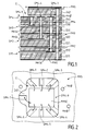
- a first dielectric layer D11 carries in the lower part a ground plane PM1, defined by metallization added to the layer. Between the layer D11 and a second dielectric layer D12 is placed a level of selective metallization SM1, which can serve as a connecting line.
- a third dielectric layer D21 carries in the lower part a ground plane PM2, hollowed out to form savings where it is crossed by metallized holes such as MH14.
- the structure is then repeated with the dielectric layer D21, the level of selective metallization SM2, the dielectric layer D22, and the ground plane PM3.
- this is repeated a fourth time with the dielectric layer D41, the level of selective metallization SM4, the dielectric layer D42 and the upper ground plane PM5, which is here illustrated at a certain distance above the dielectric layer D42 (for the sole purpose of improving the legibility of the drawing).
- Metallized holes such as MH0 pass completely through the structure, going from the ground plane PM1 to the ground plane PM5, connecting each time to the intermediate ground planes PM2, PM3, PM4.
- metallized holes such as MH14, MH24 or MH34 connect levels of conductive bonds to each other.
- the metallized holes do not in principle come into contact with the ground planes, except where it is desired.
- the metallized hole MH14 connects a conductive line of level SM1 to a conductive line of level SM4.
- the metallized hole MH24 connects a line of level SM2 to a line of level SM4. And the metallized hole MH34 connects a line of level SM3 to a line of level SM4.
- the last of the dielectric layers, here layer D42, is indented to define a clearance, which discovers the underlying level of conductive bonds.
- Each clearance is shaped as a function of the geometry of a microwave active element (or passive element) chip, the definition of the conformation being considered here as accessible to a person skilled in the art.
- the chip supply will come from another level of connection of the stack, reached by metallized holes. At least some of the inputs, outputs, or inputs / outputs of the chip can also come from a lower level of link, at least where link crossings are necessary.
- FIG. 2 illustrates in notch E an MMIC chip which has three input / output terminals connected by soldered wire ("ball bonding") to conductive lines which can be distinguished in SM4-1 to SM4-6 .
- Power is supplied by a link on another line SM4-7, while the mass of the chip is defined here by its bottom connected to the underlying conductor SM-9 by a conductive adhesive. Alternatively, the mass can be brought in by another lateral connection.
- FIG. 2 also shows through metallized holes indicated in MH0.
- triplate The structure which has just been described can be considered as the combination of four superimposed triplate systems ("stripline”), in which are incorporated in a new way the active chips or else passive elements of a technology. different.
- the circuit inputs / outputs can be defined by one or more lateral connectors (not shown). These connectors can be mounted as components, if required.
- the dielectric material is that known under the name of Duroid 6002 (registered trademark), in a thickness of 0.127 mm, sold by the company Rogers Corporation.
- This material has a dielectric constant of 2.9 to 10 GHz, for a dissipation factor of 0.013 at the same frequency.
- These thermal expansion coefficients are 16 ppm / ° K in the X and Y directions, that is to say in its plane, against 24 ppm / ° K in the Z direction, that is to say perpendicular to his plan.
- the Applicant has observed that it is possible to use this material to produce spaced apart transmission lines of width 100 ⁇ m, having a spacing between them which is also 100 ⁇ m, these dimensions being adjustable according to the desired impedance.
- the through holes can be made with a diameter of 0.3 mm, to connect to metallizations whose minimum size is that of the diameter of the hole increased by 0.3 mm.
- the diameter of the holes must be at least equal to approximately 1 / 5th of the thickness of the layers crossed.
- the starting point consists of layers of Duroid 6002, the thickness of which is either 0.127 or 0.254 mm. These layers are provided with a copper metallization, the thickness of which is 35 ⁇ m, for example.
- Figure 3 illustrates the following steps in the manufacturing process, for each of the tri-plate structures that the device comprises.
- Step 101 starts from the metallized copper sheet which has just been defined.
- Step 103 consists of drilling it in the desired places.
- Step 105 consists of the metallization of the holes.
- Step 107 consists of a selective refill of copper ("pattern plating"), adding for example at least 25 ⁇ m to the 35 ⁇ m of copper already deposited.
- Step 111 consists of a selective nickel-gold plating for the inputs / outputs of the chip, preferably also for those of the circuit).
- Step 113 consists in attacking the copper, at the desired locations either to make way for the through holes, or to ensure the transmission lines.
- Step 115 consists of hot pressing (autoclave), to ensure the high temperature bonding of the layers, which bond by fusion.
- Step 116 consists of trimming the outside of the circuit and the locations of chips or other components. This trimming is carried out for example with a milling cutter or by laser machining.
- electrolytic plating with nickel and gold is carried out not only for the inputs / outputs, but also for the solder pads by wire of the chip.
- Lateral metallizations can also be carried out on the sides of the structure, before it is cut into individual circuits, and / or on the input / output side.
- the notches intended to receive the chips or passive elements are cut a priori (before the pressing of step 115) in the upper dielectric layer of the upper tri-plate element.
- Such indentations or clearances make it possible to house, for example, passive components, or else microwave microchips based on gallium arsenide, which are directly fixed by a conductive epoxy adhesive for microelectronics (such as the H20E adhesive from the company EPOTECNY from the United States), over an area with a 70 ⁇ m thick metallization. Two blind holes placed under the chip allow the ground connection.
- Wire welding on the terminals of the chip is carried out after the adhesive has polymerized.
- a thermosonic gold ball bonding process is used, with a wire diameter of 25 ⁇ m.
- thermosonic tape 75 ⁇ m wide which can allow a shorter loop and a lower inductance.
Landscapes
- Engineering & Computer Science (AREA)
- Microelectronics & Electronic Packaging (AREA)
- Die Bonding (AREA)
- Waveguides (AREA)
- Semiconductor Integrated Circuits (AREA)
Applications Claiming Priority (2)
| Application Number | Priority Date | Filing Date | Title |
|---|---|---|---|
| FR9511609 | 1995-10-03 | ||
| FR9511609A FR2739492B1 (fr) | 1995-10-03 | 1995-10-03 | Circuit hyperfrequence multi-couches a elements actifs integres |
Publications (1)
| Publication Number | Publication Date |
|---|---|
| EP0767496A1 true EP0767496A1 (de) | 1997-04-09 |
Family
ID=9483180
Family Applications (1)
| Application Number | Title | Priority Date | Filing Date |
|---|---|---|---|
| EP96402062A Ceased EP0767496A1 (de) | 1995-10-03 | 1996-09-27 | Mehrschicht-Hochfrequenzschaltung mit integrierten aktiven Elementen |
Country Status (2)
| Country | Link |
|---|---|
| EP (1) | EP0767496A1 (de) |
| FR (1) | FR2739492B1 (de) |
Cited By (3)
| Publication number | Priority date | Publication date | Assignee | Title |
|---|---|---|---|---|
| US6099677A (en) * | 1998-02-13 | 2000-08-08 | Merrimac Industries, Inc. | Method of making microwave, multifunction modules using fluoropolymer composite substrates |
| US9230726B1 (en) | 2015-02-20 | 2016-01-05 | Crane Electronics, Inc. | Transformer-based power converters with 3D printed microchannel heat sink |
| US9888568B2 (en) | 2012-02-08 | 2018-02-06 | Crane Electronics, Inc. | Multilayer electronics assembly and method for embedding electrical circuit components within a three dimensional module |
Citations (5)
| Publication number | Priority date | Publication date | Assignee | Title |
|---|---|---|---|---|
| WO1984001470A1 (en) * | 1982-10-05 | 1984-04-12 | Mayo Foundation | Leadless chip carrier for logic components |
| EP0198698A2 (de) * | 1985-04-13 | 1986-10-22 | Fujitsu Limited | Integrierte Schaltung mit eingebauter Streifenleiterstruktur |
| GB2189084A (en) * | 1986-04-10 | 1987-10-14 | Stc Plc | Integrated circuit packaging |
| EP0595346A1 (de) * | 1992-10-29 | 1994-05-04 | Nec Corporation | Modulare Mikrowellen-Anordnungseinheit und seine Verbindungsstruktur |
| US5311406A (en) * | 1991-10-30 | 1994-05-10 | Honeywell Inc. | Microstrip printed wiring board and a method for making same |
-
1995
- 1995-10-03 FR FR9511609A patent/FR2739492B1/fr not_active Expired - Fee Related
-
1996
- 1996-09-27 EP EP96402062A patent/EP0767496A1/de not_active Ceased
Patent Citations (5)
| Publication number | Priority date | Publication date | Assignee | Title |
|---|---|---|---|---|
| WO1984001470A1 (en) * | 1982-10-05 | 1984-04-12 | Mayo Foundation | Leadless chip carrier for logic components |
| EP0198698A2 (de) * | 1985-04-13 | 1986-10-22 | Fujitsu Limited | Integrierte Schaltung mit eingebauter Streifenleiterstruktur |
| GB2189084A (en) * | 1986-04-10 | 1987-10-14 | Stc Plc | Integrated circuit packaging |
| US5311406A (en) * | 1991-10-30 | 1994-05-10 | Honeywell Inc. | Microstrip printed wiring board and a method for making same |
| EP0595346A1 (de) * | 1992-10-29 | 1994-05-04 | Nec Corporation | Modulare Mikrowellen-Anordnungseinheit und seine Verbindungsstruktur |
Cited By (5)
| Publication number | Priority date | Publication date | Assignee | Title |
|---|---|---|---|---|
| US6099677A (en) * | 1998-02-13 | 2000-08-08 | Merrimac Industries, Inc. | Method of making microwave, multifunction modules using fluoropolymer composite substrates |
| US6395374B1 (en) | 1998-02-13 | 2002-05-28 | Merrimac Industries, Inc. | Method of making microwave, multifunction modules using fluoropolymer composite substrates |
| US9888568B2 (en) | 2012-02-08 | 2018-02-06 | Crane Electronics, Inc. | Multilayer electronics assembly and method for embedding electrical circuit components within a three dimensional module |
| US11172572B2 (en) | 2012-02-08 | 2021-11-09 | Crane Electronics, Inc. | Multilayer electronics assembly and method for embedding electrical circuit components within a three dimensional module |
| US9230726B1 (en) | 2015-02-20 | 2016-01-05 | Crane Electronics, Inc. | Transformer-based power converters with 3D printed microchannel heat sink |
Also Published As
| Publication number | Publication date |
|---|---|
| FR2739492A1 (fr) | 1997-04-04 |
| FR2739492B1 (fr) | 1997-11-07 |
Similar Documents
| Publication | Publication Date | Title |
|---|---|---|
| JP2905736B2 (ja) | 半導体装置 | |
| KR100773615B1 (ko) | 반도체 장치 및 그 제조 방법 | |
| US7884458B2 (en) | Decoupling capacitor, wafer stack package including the decoupling capacitor, and method of fabricating the wafer stack package | |
| FR2724054A1 (fr) | Structure de montage de boitier semiconducteur | |
| FR2778024A1 (fr) | Structure de connexion pour lignes de guide d'ondes dielectrique | |
| TW201025719A (en) | Integrated circuit structure | |
| EP1312116A1 (de) | Verteiltes abschirmungs- und/oder entkopplungsverfahren für vorrichtung mit dreidimensionaler verdrahtungsstruktur | |
| FR2983638A1 (fr) | Procede de formation d'un circuit integre | |
| TWI359467B (en) | Via structure of packages for high frequency semic | |
| FR2735648A1 (fr) | Procede de refroidissement d'un circuit integre monte dans un boitier | |
| EP4141915A1 (de) | Verfahren zur herstellung eines verkapselten mikrochips im chipmassstab sowie die entsprechende vorrichtung | |
| FR2911006A1 (fr) | Puce de circuit electronique integre comprenant une inductance | |
| EP0191668B1 (de) | Keramischer Hochfrequenzmehrschichtkondensator mit hoher Kapazität | |
| FR2739492A1 (fr) | Circuit hyperfrequence multi-couches a elements actifs integres | |
| EP0795907A1 (de) | Mehrlagige Hochfrequenzschaltung mit integrierten aktiven Elementen | |
| US5932926A (en) | Microwave semiconductor integrated circuit | |
| FR3123147A1 (fr) | Boîtier de circuit intégré à puce retournée de type à matrice de billes pour fonctionnement à très haute fréquence. | |
| GB2189084A (en) | Integrated circuit packaging | |
| FR2547112A1 (fr) | Procede de realisation d'un circuit hybride et circuit hybride logique ou analogique | |
| JP2006042098A (ja) | 高周波用配線基板 | |
| FR2529385A1 (fr) | Microboitier d'encapsulation de circuits integres logiques fonctionnant en tres haute frequence | |
| FR2739496A1 (fr) | Circuit hyperfrequence multicouches a elements actifs integres | |
| EP2688137B1 (de) | Hyperfrequenzresonator mit Impedanzsprung, insbesondere für Hyperfrequenz-Bandsperrfilter oder -Bandpassfilter | |
| FR2837982A1 (fr) | Module de circuits integres et procede de fabrication correspondant | |
| CN113972200A (zh) | 半导体结构及其制备方法 |
Legal Events
| Date | Code | Title | Description |
|---|---|---|---|
| PUAI | Public reference made under article 153(3) epc to a published international application that has entered the european phase |
Free format text: ORIGINAL CODE: 0009012 |
|
| AK | Designated contracting states |
Kind code of ref document: A1 Designated state(s): DE GB IT SE |
|
| 17P | Request for examination filed |
Effective date: 19970613 |
|
| 17Q | First examination report despatched |
Effective date: 19990716 |
|
| STAA | Information on the status of an ep patent application or granted ep patent |
Free format text: STATUS: THE APPLICATION HAS BEEN REFUSED |
|
| 18R | Application refused |
Effective date: 20000526 |