EP0768718A2 - Feldeffekttransistor mit kurzer Kanallänge - Google Patents
Feldeffekttransistor mit kurzer Kanallänge Download PDFInfo
- Publication number
- EP0768718A2 EP0768718A2 EP96116151A EP96116151A EP0768718A2 EP 0768718 A2 EP0768718 A2 EP 0768718A2 EP 96116151 A EP96116151 A EP 96116151A EP 96116151 A EP96116151 A EP 96116151A EP 0768718 A2 EP0768718 A2 EP 0768718A2
- Authority
- EP
- European Patent Office
- Prior art keywords
- semiconductor layer
- face
- layer
- current guiding
- adjacent
- Prior art date
- Legal status (The legal status is an assumption and is not a legal conclusion. Google has not performed a legal analysis and makes no representation as to the accuracy of the status listed.)
- Withdrawn
Links
Images


Classifications
-
- H—ELECTRICITY
- H10—SEMICONDUCTOR DEVICES; ELECTRIC SOLID-STATE DEVICES NOT OTHERWISE PROVIDED FOR
- H10D—INORGANIC ELECTRIC SEMICONDUCTOR DEVICES
- H10D30/00—Field-effect transistors [FET]
- H10D30/01—Manufacture or treatment
- H10D30/021—Manufacture or treatment of FETs having insulated gates [IGFET]
- H10D30/0223—Manufacture or treatment of FETs having insulated gates [IGFET] having source and drain regions or source and drain extensions self-aligned to sides of the gate
-
- H—ELECTRICITY
- H10—SEMICONDUCTOR DEVICES; ELECTRIC SOLID-STATE DEVICES NOT OTHERWISE PROVIDED FOR
- H10D—INORGANIC ELECTRIC SEMICONDUCTOR DEVICES
- H10D30/00—Field-effect transistors [FET]
- H10D30/60—Insulated-gate field-effect transistors [IGFET]
- H10D30/637—Lateral IGFETs having no inversion channels, e.g. buried channel lateral IGFETs, normally-on lateral IGFETs or depletion-mode lateral IGFETs
-
- H—ELECTRICITY
- H10—SEMICONDUCTOR DEVICES; ELECTRIC SOLID-STATE DEVICES NOT OTHERWISE PROVIDED FOR
- H10D—INORGANIC ELECTRIC SEMICONDUCTOR DEVICES
- H10D62/00—Semiconductor bodies, or regions thereof, of devices having potential barriers
- H10D62/10—Shapes, relative sizes or dispositions of the regions of the semiconductor bodies; Shapes of the semiconductor bodies
- H10D62/17—Semiconductor regions connected to electrodes not carrying current to be rectified, amplified or switched, e.g. channel regions
- H10D62/213—Channel regions of field-effect devices
- H10D62/221—Channel regions of field-effect devices of FETs
- H10D62/235—Channel regions of field-effect devices of FETs of IGFETs
- H10D62/299—Channel regions of field-effect devices of FETs of IGFETs having lateral doping variations
- H10D62/307—Channel regions of field-effect devices of FETs of IGFETs having lateral doping variations the doping variations being parallel to the channel lengths
-
- H—ELECTRICITY
- H10—SEMICONDUCTOR DEVICES; ELECTRIC SOLID-STATE DEVICES NOT OTHERWISE PROVIDED FOR
- H10D—INORGANIC ELECTRIC SEMICONDUCTOR DEVICES
- H10D62/00—Semiconductor bodies, or regions thereof, of devices having potential barriers
- H10D62/10—Shapes, relative sizes or dispositions of the regions of the semiconductor bodies; Shapes of the semiconductor bodies
- H10D62/17—Semiconductor regions connected to electrodes not carrying current to be rectified, amplified or switched, e.g. channel regions
- H10D62/213—Channel regions of field-effect devices
- H10D62/221—Channel regions of field-effect devices of FETs
- H10D62/235—Channel regions of field-effect devices of FETs of IGFETs
- H10D62/314—Channel regions of field-effect devices of FETs of IGFETs having vertical doping variations
-
- H—ELECTRICITY
- H10—SEMICONDUCTOR DEVICES; ELECTRIC SOLID-STATE DEVICES NOT OTHERWISE PROVIDED FOR
- H10D—INORGANIC ELECTRIC SEMICONDUCTOR DEVICES
- H10D62/00—Semiconductor bodies, or regions thereof, of devices having potential barriers
- H10D62/10—Shapes, relative sizes or dispositions of the regions of the semiconductor bodies; Shapes of the semiconductor bodies
- H10D62/17—Semiconductor regions connected to electrodes not carrying current to be rectified, amplified or switched, e.g. channel regions
- H10D62/351—Substrate regions of field-effect devices
- H10D62/357—Substrate regions of field-effect devices of FETs
- H10D62/364—Substrate regions of field-effect devices of FETs of IGFETs
- H10D62/371—Inactive supplementary semiconductor regions, e.g. for preventing punch-through, improving capacity effect or leakage current
Definitions
- This invention is related in general to the field of semiconductor devices. More particularly, the invention is related to semiconductor devices with super-steep retrograde and/or pocket implant and/or counter doping.
- a low threshold voltage transistor with improved performance is provided which eliminates or substantially reduces the disadvantages associated with prior transistor devices.
- a transistor is formed in a face of a semiconductor.
- the transistor includes source and drain regions formed in the face of the semiconductor layer with a gate insulatively disposed adjacent the face of the semiconductor layer and between the source and drain regions.
- a layer of counter doping is introduced in and near the face of the semiconductor layer generally between the source and drain regions.
- Two pocket implants may also be formed generally adjacent to the source and/or drain regions and the counter doped layer.
- a method of manufacturing a transistor is provided.
- the transistor is formed in a face of a semiconductor layer having a first conductivity type.
- the method includes the steps of selectively implanting a shallow layer of impurities of a second conductivity type adjacent to the face of the semiconductor layer and forming pockets of impurities of the first conductivity type generally adjacent to the source and drain regions below the gate.
- the pockets may also be formed closer to the face of the semiconductor layer with the layer of counter doping therebetween.
- a transistor structure in yet another aspect of the invention, includes a surface counter doping layer of the second impurity type formed generally between the drain and source regions, and pocket implants of the first impurity type formed generally adjacent and/or below the counter doping layer.
- a transistor is formed in a face of a semiconductor.
- the transistor includes source and drain regions formed in the face of the semiconductor layer with a gate insulatively disposed adjacent the face of the semiconductor layer and between the source and drain regions.
- a super-steep retrograde channel doping profile is disposed in the semiconductor layer a predetermined distance from the face of the semiconductor layer, and a layer of counter doping is introduced in and near the face of the semiconductor layer generally between the source and drain regions.
- two pocket implants may also be formed generally adjacent to the source and/or drain regions and the counter doped layer.
- a method of manufacturing a transistor is provided.
- the transistor is formed in a face of a semiconductor layer having a first conductivity type.
- the method includes the steps of implanting impurities of the first conductivity type to form a super-steep retrograde channel profile at a predetermined distance below the face of the semiconductor layer, and selectively implanting a shallow layer of impurities of a second conductivity type adjacent to the face of the semiconductor layer.
- pockets of impurities of the first conductivity type are implanted generally adjacent to the source and drain regions below the gate.
- inventions include a submission transistor structure that has low threshold voltage satisfying the need for high performance at lower power supply voltages for portable electronic equipment.
- the instant transistor structure(s) satisfies this need with a reduced short channel effect which in turn minimizes the sensitivity of transistor performance to gate length variation at shorter channel lengths.
- FIGURES 1-6 The preferred embodiment(s) of the present invention is (are) illustrated in FIGURES 1-6, like reference numerals being used to refer to like and corresponding parts of the various drawings.
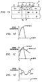
- an nMOS transistor structure 10 includes a gate electrode 12, gate dielectric 14, and source and drain n ++ regions 16 and 18.
- a p + super-steep retrograde (SSR) channel 20 is further formed at a predetermined distance or depth from the top surface of the device in a p-type substrate or well structure 22.
- SSR super-steep retrograde
- 190 Kev indium (In) at a dose of 1 x 10 13 cm -2 may be implanted in an nMOS region to form the super-steep retrograde channel 20.
- the n + super-steep retrograde channel 20 may be formed by implanting arsenic (As).
- super-steep retrograde channel profile When compared with conventional channel doping profiles using boron (B) for nMOS and Phosphorus (P) for pMOS, for example, super-steep retrograde channel profile has been shown to provide better short channel integrity. Further, super-steep retrograde channel doping also provides a higher channel mobility due to lower surface doping.
- B boron
- P Phosphorus
- FIGURE 1B is an exemplary plot of doping concentration versus depth for transistor structure 10 along Y-Y'
- FIGURE 1C is an exemplary plot of doping concentration along Y 2 -Y 2 '
- FIGURE 1D is an exemplary plot of surface doping concentration along X-X'.
- Transistor structure 10 with both super-steep retrograde channel doping 20 and pocket implants 24 has reduced short-channel effect when compared to a super-steep retrograde only channel profile, described in technical articles such as "Indium Channel Implant for Improved Short-Channel Behavior of Submicrometer NMOSFET's" by Shahidi et al. in IEEE Electron Device Letters , Vol. 14, No. 8, p. 409, August 1993; and "Tradeoffs of Current Drive vs. Short-Channel Effect in Deep-Submicrometer Bulk and SOI MOSFETs" by Su et al. in IEEE IEDM , p. 649, 1994.
- Transistor structure 10 also has better short channel integrity when compared to a conventional device with pocket implants described in Rodder et al.
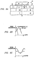
- Transistor structure 30 is shown as an nMOS with a gate electrode 32, gate dielectric 34, and source and drain n ++ regions 36 and 38.
- a p-type super-steep retrograde buried channel 40 is formed at a predetermined depth in a p-type substrate or well formation 42.
- a narrow layer 44 of surface counter doping of n-type (n + ) is formed in the region between source and drain regions 36 and 38 and below gate 32.
- the counter doping may be formed with, for example, arsenic (As) at a dosage of 2 to 4 x 10 12 cm -2 for nMOS or BF 2 for pMOS (not shown).
- FIGURE 2B is an exemplary plot of doping concentration versus depth of transistor structure 30 taken along Y-Y'
- FIGURE 2C is an exemplary plot of surface doping concentration along X-X'. Counter doping is discussed in articles such as "High Performance Sub-0.1- ⁇ m CMOS with Low-Resistance T-shaped Gates Fabricated by Selective CVD-W" by Hisamoto et al.
- Transistor structure 30 combining super-steep retrograde channel 40 and surface counter doping 44 lowers the threshold voltage and maintains good short channel effect.
- the counter doping 44 provides threshold voltage scaling to the desired range of approximately 0.05 to 0.15 volts, while the underlying super-steep retrograde channel profile 40 is more effective at reducing threshold voltage roll-off than conventional well and channel profile described in Hisamoto et al.
- Transistor structure 30 also maintains high nominal drive current due to its low threshold voltage and high effective electron mobility ⁇ eff . Therefore, the combination of these features provides optimal performance for low supply voltage CMOS applications.
- Transistor structure 50 with a super-steep retrograde channel profile, pocket implantation, and counter doping is shown.
- Transistor structure 50 is shown as an nMOS and includes a gate electrode 52, gate dielectric 54, and source and drain regions 56 and 58.
- a super-steep retrograde channel 60 is implanted subsurface generally below source and drain regions 56 and 58 in a substrate or well structure 62.
- Pockets 64 are implanted at a shallow depth near the surface and adjacent to source and drain regions 56 and 58.
- Surface counter doping 66 is also formed generally between implanted pockets 64.
- FIGURE 3B An exemplary doping concentration versus depth plot for transistor 50 along Y-Y' is shown in FIGURE 3B, and another exemplary plot of doping concentration along Y 2 -Y 2 ' is shown in FIGURE 3C.
- FIGURE 3D A surface doping concentration plot along X-X' of transistor structure 50 is shown in FIGURE 3D.
- FIGURE 4A shows one possible variation of the placement of pocket implants with respect to counter doping.
- Transistor 50' includes pocket implants 64' that are slightly subsurface below the counter doped layer 66'.
- An exemplary doping concentration versus depth plot along Y-Y' for transistor 50' is shown in FIGURE 4B, surface doping concentration along X-X' is shown in FIGURE 4C, and doping concentration along Y 2 -Y 2 ' is shown in FIGURE 4D.
- Transistor structures 50 and 50' combine the advantages of super-steep retrograde channel, pocket implants, and surface counter doping and are both well-suited to low power applications due to their low threshold voltage, reduced short channel effect, and good drive current.
- FIGURE 5A is a cross-sectional view of a transistor structure 70 that does not incorporate a super-steep retrograde channel profile and yet still has low threshold voltage and improved short channel effect.
- Transistor structure 70 includes a gate electrode 72, gate dielectric 74, and source and drain n ++ regions 76 and 78.
- Transistor structure 70 further includes a surface counter doping n + layer 80 in combination with pocket implants 82 and 84 of an opposite type (p + ). As discussed above, the placement of surface counter doping layer 80 and pocket implants 82 and 84 may have a number of variations, all of which are contemplated herein.
- Exemplary doping concentration in transistor 70 along lines Y-Y' and Y 2 -Y 2 ' are shown in FIGURES 5B and 5C, respectively.
- An exemplary surface doping concentration of transistor structure 70 along X-X' is shown in FIGURE 5D.
- FIGURE 6A is a cross-sectional view of yet another transistor structure 70' with counter doping and pocket implants.
- Transistor structure 70' includes a gate electrode 72, gate dielectric 74, and source and drain n ++ regions 76 and 78.
- Transistor structure 70' further includes a surface counter doping n + layer 80' in combination with pocket implants 82' and 84' of an opposite type (p + ).
- p + opposite type
- the placement of surface counter doping layer 80' and pocket implants 82' and 84' may have a number of variations, all of which are contemplated herein.
- the pocket implants 82 and 84 of FIGURE 5A are formed generally below the counter doping layer 80, but the pocket implants 82' and 84' are formed near the surface.
- Exemplary doping concentration in transistor 70' along lines Y-Y' and Y 2 -Y 2 ' are shown in FIGURES 6B and 6C, respectively.
- An exemplary surface doping concentration of transistor structure 70 along X-X' is shown in FIGURE 6D.
- Transistors 10, 30, 50, 50', 70, and 70' may be constructed by conventional semiconductor processing technology and may include forming the super-steep retrograde channel, the gate, and drain and source regions. The counted doping may be formed before the formation of the gate. Pocket implant may be formed after gate formation.
Landscapes
- Thin Film Transistor (AREA)
- Insulated Gate Type Field-Effect Transistor (AREA)
- Metal-Oxide And Bipolar Metal-Oxide Semiconductor Integrated Circuits (AREA)
Applications Claiming Priority (4)
| Application Number | Priority Date | Filing Date | Title |
|---|---|---|---|
| US521695P | 1995-10-09 | 1995-10-09 | |
| US521595P | 1995-10-09 | 1995-10-09 | |
| US5215 | 1995-10-09 | ||
| US5216 | 1995-10-09 |
Publications (2)
| Publication Number | Publication Date |
|---|---|
| EP0768718A2 true EP0768718A2 (de) | 1997-04-16 |
| EP0768718A3 EP0768718A3 (de) | 1998-07-08 |
Family
ID=26674081
Family Applications (1)
| Application Number | Title | Priority Date | Filing Date |
|---|---|---|---|
| EP96116151A Withdrawn EP0768718A3 (de) | 1995-10-09 | 1996-10-09 | Feldeffekttransistor mit kurzer Kanallänge |
Country Status (3)
| Country | Link |
|---|---|
| EP (1) | EP0768718A3 (de) |
| KR (1) | KR970023883A (de) |
| TW (1) | TW388088B (de) |
Cited By (3)
| Publication number | Priority date | Publication date | Assignee | Title |
|---|---|---|---|---|
| GB2355851A (en) * | 1999-06-24 | 2001-05-02 | Lucent Technologies Inc | Short gate/channel MOSFET |
| US6740912B1 (en) | 1999-06-24 | 2004-05-25 | Agere Systems Inc. | Semiconductor device free of LLD regions |
| US7671425B2 (en) | 1998-02-05 | 2010-03-02 | Semiconductor Energy Laboratory Co., Ltd. | Semiconductor device and method of manufacturing the same |
Family Cites Families (4)
| Publication number | Priority date | Publication date | Assignee | Title |
|---|---|---|---|---|
| US4242691A (en) * | 1978-09-18 | 1980-12-30 | Mitsubishi Denki Kabushiki Kaisha | MOS Semiconductor device |
| US5270226A (en) * | 1989-04-03 | 1993-12-14 | Matsushita Electric Industrial Co., Ltd. | Manufacturing method for LDDFETS using oblique ion implantion technique |
| JP2578662B2 (ja) * | 1989-05-19 | 1997-02-05 | 三洋電機株式会社 | 半導体装置の製造方法 |
| US5536957A (en) * | 1990-01-16 | 1996-07-16 | Mitsubishi Denki Kabushiki Kaisha | MOS field effect transistor having source/drain regions surrounded by impurity wells |
-
1996
- 1996-10-09 KR KR1019960044740A patent/KR970023883A/ko not_active Ceased
- 1996-10-09 EP EP96116151A patent/EP0768718A3/de not_active Withdrawn
- 1996-12-20 TW TW085115732A patent/TW388088B/zh active
Cited By (4)
| Publication number | Priority date | Publication date | Assignee | Title |
|---|---|---|---|---|
| US7671425B2 (en) | 1998-02-05 | 2010-03-02 | Semiconductor Energy Laboratory Co., Ltd. | Semiconductor device and method of manufacturing the same |
| GB2355851A (en) * | 1999-06-24 | 2001-05-02 | Lucent Technologies Inc | Short gate/channel MOSFET |
| GB2355851B (en) * | 1999-06-24 | 2003-11-19 | Lucent Technologies Inc | MOS Transistor |
| US6740912B1 (en) | 1999-06-24 | 2004-05-25 | Agere Systems Inc. | Semiconductor device free of LLD regions |
Also Published As
| Publication number | Publication date |
|---|---|
| EP0768718A3 (de) | 1998-07-08 |
| TW388088B (en) | 2000-04-21 |
| KR970023883A (ko) | 1997-05-30 |
Similar Documents
| Publication | Publication Date | Title |
|---|---|---|
| US6228725B1 (en) | Semiconductor devices with pocket implant and counter doping | |
| US5985705A (en) | Low threshold voltage MOS transistor and method of manufacture | |
| EP0752722B1 (de) | FET mit stabiler Schwellwertspannung und dessen Herstellungsverfahren | |
| US5548143A (en) | Metal oxide semiconductor transistor and a method for manufacturing the same | |
| US7180136B2 (en) | Biased, triple-well fully depleted SOI structure | |
| JP4470011B2 (ja) | ゲート電極を備えたトランジスタを有するデバイス及びその形成方法 | |
| US6563151B1 (en) | Field effect transistors having gate and sub-gate electrodes that utilize different work function materials and methods of forming same | |
| US5963799A (en) | Blanket well counter doping process for high speed/low power MOSFETs | |
| EP0970513A2 (de) | Erhöhte schwelspannung zur verbesserung der wanne | |
| US20080283922A1 (en) | Semiconductor device and manufacturing method thereof | |
| US10217838B2 (en) | Semiconductor structure with multiple transistors having various threshold voltages | |
| US20080121992A1 (en) | Semiconductor device including diffusion barrier region and method of fabricating the same | |
| US6583013B1 (en) | Method for forming a mixed voltage circuit having complementary devices | |
| US6667512B1 (en) | Asymmetric retrograde halo metal-oxide-semiconductor field-effect transistor (MOSFET) | |
| EP0768718A2 (de) | Feldeffekttransistor mit kurzer Kanallänge | |
| US5731612A (en) | Insulated gate field effect transistor structure having a unilateral source extension | |
| EP0870332B1 (de) | Verfahren zur Herstellung einer MOSFET-Halbleiteranordnung mit vermindertem Gateoxidfeld im Aus-Zustand | |
| US7560779B2 (en) | Method for forming a mixed voltage circuit having complementary devices | |
| US20050170576A1 (en) | Transistor with reduced short channel effects and method | |
| US20020068409A1 (en) | Method of reducing junction capacitance | |
| US5937302A (en) | Method of forming lightly doped drain region and heavily doping a gate using a single implant step | |
| JPH09246553A (ja) | 短チャンネルトランジスタおよびその作成方法 | |
| JPH09252132A (ja) | トランジスタ | |
| JPH10303411A (ja) | 半導体装置の製造方法 |
Legal Events
| Date | Code | Title | Description |
|---|---|---|---|
| PUAI | Public reference made under article 153(3) epc to a published international application that has entered the european phase |
Free format text: ORIGINAL CODE: 0009012 |
|
| AK | Designated contracting states |
Kind code of ref document: A2 Designated state(s): DE FR GB IT NL |
|
| PUAL | Search report despatched |
Free format text: ORIGINAL CODE: 0009013 |
|
| AK | Designated contracting states |
Kind code of ref document: A3 Designated state(s): DE FR GB IT NL |
|
| 17P | Request for examination filed |
Effective date: 19990104 |
|
| STAA | Information on the status of an ep patent application or granted ep patent |
Free format text: STATUS: THE APPLICATION IS DEEMED TO BE WITHDRAWN |
|
| 18D | Application deemed to be withdrawn |
Effective date: 20030501 |