EP0768762A1 - Ausgangsschaltung - Google Patents
Ausgangsschaltung Download PDFInfo
- Publication number
- EP0768762A1 EP0768762A1 EP96116613A EP96116613A EP0768762A1 EP 0768762 A1 EP0768762 A1 EP 0768762A1 EP 96116613 A EP96116613 A EP 96116613A EP 96116613 A EP96116613 A EP 96116613A EP 0768762 A1 EP0768762 A1 EP 0768762A1
- Authority
- EP
- European Patent Office
- Prior art keywords
- output
- terminal
- transistor
- channel mos
- gate
- Prior art date
- Legal status (The legal status is an assumption and is not a legal conclusion. Google has not performed a legal analysis and makes no representation as to the accuracy of the status listed.)
- Granted
Links
Images


Classifications
-
- H—ELECTRICITY
- H03—ELECTRONIC CIRCUITRY
- H03K—PULSE TECHNIQUE
- H03K17/00—Electronic switching or gating, i.e. not by contact-making and –breaking
- H03K17/14—Modifications for compensating variations of physical values, e.g. of temperature
- H03K17/145—Modifications for compensating variations of physical values, e.g. of temperature in field-effect transistor switches
-
- H—ELECTRICITY
- H03—ELECTRONIC CIRCUITRY
- H03K—PULSE TECHNIQUE
- H03K17/00—Electronic switching or gating, i.e. not by contact-making and –breaking
- H03K17/51—Electronic switching or gating, i.e. not by contact-making and –breaking characterised by the components used
- H03K17/56—Electronic switching or gating, i.e. not by contact-making and –breaking characterised by the components used by the use, as active elements, of semiconductor devices
- H03K17/687—Electronic switching or gating, i.e. not by contact-making and –breaking characterised by the components used by the use, as active elements, of semiconductor devices the devices being field-effect transistors
- H03K17/6871—Electronic switching or gating, i.e. not by contact-making and –breaking characterised by the components used by the use, as active elements, of semiconductor devices the devices being field-effect transistors the output circuit comprising more than one controlled field-effect transistor
- H03K17/6872—Electronic switching or gating, i.e. not by contact-making and –breaking characterised by the components used by the use, as active elements, of semiconductor devices the devices being field-effect transistors the output circuit comprising more than one controlled field-effect transistor using complementary field-effect transistors
-
- H—ELECTRICITY
- H03—ELECTRONIC CIRCUITRY
- H03K—PULSE TECHNIQUE
- H03K19/00—Logic circuits, i.e. having at least two inputs acting on one output; Inverting circuits
- H03K19/003—Modifications for increasing the reliability for protection
- H03K19/00315—Modifications for increasing the reliability for protection in field-effect transistor circuits
Definitions
- the present invention relates to an output circuit and, particularly, to an output circuit of an integrated circuit which has an output terminal applied with a voltage higher than a source voltage thereof and is operable at a low voltage.
- the output circuit includes an over-voltage protection circuit for preventing current from flowing from the side of the high potential LSI to the lower potential LSI to restrict variations of the source voltage and current of the lower potential LSI.
- the conventional output circuit includes inverters 1 and 2 having inputs connected to an input terminal TI, an output buffer circuit 4 which is adapted to be driven by these inverters 1 and 2 and output an output signal in response to output signal from the inverters 1 and 2 at an output terminal TO and a protection circuit 7 which is adapted to cut off the output transistor P1 when an over-voltage is applied to the output terminal TO to thereby prevent current from flowing thereinto.
- the output buffer circuit 4 includes a PMOS transistor P1 having a source connected to a power source VDD, a gate connected to an output of the inverter 1 and a drain connected to the output terminal TO and an NMOS transistor N6 having a source grounded to GND, a gate connected to an output terminal of the inverter 2 and a drain connected to the output terminal TO.
- the protection circuit 7 includes a PMOS type transistor P15 having a source connected to the output of the inverter 1 through the terminal a, a gate connected to the power source VDD through the terminal b and a drain connected to the terminal e, a PMOS type transistor P16 having a source connected to the terminal b, a gate connected to the output terminal TO through the terminal e and a drain and an well connected each other and further connected to the wells of the transistors P1 and P15 through the terminal c, respectively, and a PMOS type transistor P17 having a source connected to the output of the inverter 1 through the terminal a, a gate connected to the input terminal TI through the terminal d and a drain and an well connected each other and further connected to the well of the transistor P16.
- the well potential when a well potential of the PMOS type transistor is lower than its source potential, not only a threshold value of the transistor varies but also a current path is formed from the source to a substrate, which cause the transistor itself to be degraded and cause a power consumption of a circuit including the transistor. Therefore, the well potential must be substantially the same as the source potential.
- the protection circuit 7 is provided to prevent the current path described above from being formed as the following.
- the transistor P15 turns on because the source potential thereof becomes higher than a gate potential thereof. Therefore, the potential VPP supplied to the terminal TO is propagated to the gate electrode of the transistor P1 through the transistor P15 to thereby cut off the transistor P1.
- the transistor P17 is provided to make the well potentials of P1 and P15 to equal to the corresponding source potentials of P1 and P15, respectively, to thereby prevent current flowing between the well region and the source region.
- the transistor P16 is provided to maintain the well potentials equal to the power source potential VDD when the output terminal TO is a ground potential GND.
- the inverter When the output buffer outputs VDD level, the inverter outputs L level (ground level GND) to turn on P1. Therefore, a N-channel transistor of the inverter is in ON state. As a result, a current path from the terminal TO to the ground line through P15 and the N-channel transistor of tee inverter is made.
- the output transistor having large channel width is used in the output buffer thereof.
- the drive inverter is formed by using transistor having large channel width. Therefore, the current flowing from the output terminal TO to the ground GND becomes large, causing the problem of current consumption and heat generation to occur.
- An object of the present invention is to provide an output circuit which is free from the problem of current consumption and heat generation when a potential higher than a potential of a power source of the output circuit is applied to an output terminal of the output circuit which is operating at the source potential.
- an output circuit which has an output buffer circuit including a first and second transistors responsive to a high and low levels of an input signal to switch a level of an output signal output at an output terminal to a power source or a ground and a protection circuit for turning the first transistor OFF when an over-voltage higher than the power source voltage is applied to the output terminal, comprises:
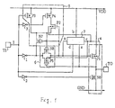
- FIG. 1 shows an embodiment of the present invention, in which constructive elements commonly used in Fig. 4 are depicted by the same reference numerals, respectively.
- An output circuit shown in Fig. 1 comprises, in addition to inverters 1 and 2, an output buffer circuit 4 and a protection circuit 7 which are common in Fig. 4, an inverter 3 having an input connected to an input terminal TI, a protection control circuit 5 and a transfer gate 6 having an input connected to an output of the inverter 1 and an output connected to a gate of a transistor P1 of the output buffer circuit 4.
- the protection control circuit 5 includes a PMOS type transistor P3 having a source connected to a power source VDD and a gate connected to the input terminal TI, a PMOS transistor P4 having a source connected to the power source VDD and a gate connected to the output of the inverter 3, a transistor P2 having a source connected to a drain of the transistor P4, a gate connected to the output of the transfer gate 6 and the gate of the transistor P1, a drain connected to the drain of the transistor P3 and a well connected to the well of the transistor P1 and an NMOS transistor N7 having a source connected to the output of the inverter 3, a gate connected to the gate of the transistor P2 and a drain connected to the drain of the transistor P2.
- the transfer gate 6 includes a PMOS transistor P5 having a gate connected to the output terminal TO and a well connected to the well of the transistor P1 and an NMOS transistor N8 having a gate connected to the drain of the transistor P2 and a source and a drain connected, respectively, to the source and the drain of the transistor P5 to form an input and an output thereof.
- the protection circuit 7 is the same as that of the conventional output circuit except that a terminal a is connected to the output of the transfer gate 6.
- the input terminal is supplied with an input signal having an amplitude from a L level corresponding substantially to the ground potential to a H level corresponding substantially to the power source potential VDD.
- the transistor P3 is switched from ON to OFF and each of the outputs of the inverters 1, 2 and 3 is changed from H level to L level. Therefore, the transistor P4 of the protection control circuit 5 is switched from OFF to ON and the transistor N6 is switched from ON to OFF.
- the gate of the transistor P5 of the transfer gate 6 is still supplied with a low potential from the output terminal TO so that the transistor P5 is still in the ON state.
- the L level output of the inverter 1 is supplied to the gate of the transistor P1 to turn the transistor P1 ON to thereby change the level of the output terminal TO from L to H level.
- the transistor P2 of the protection control circuit 5 is turned ON and the source potential VDD is supplied to the gate of the transistor N8 through the transistors P4 and P2. Therefore, the ON state of the transistor N8 is maintained. Since, the transistor N8 is kept ON even when the output terminal TO becomes the high potential so that the transistor P5 is turned OFF, the output terminal TO is maintained at H level.
- the transistor P1 is turned OFF so that the current path from TO to VDD is cut off because the H level of TO is supplied through P15 of the protection circuit 7 to the gate electrode of P1.
- the transistor P2 of the protection control circuit 5 is turned OFF and the transistor N7 is turned ON to discharge the gate of the transistor N8 to thereby turn N8 OFF quickly. Since the transistor P5 connected in parallel to the transistor N8 has been turned OFF at the time when the potential of the output terminal TO was changed from the L level to the H level, the transfer gate 6 constituted with the transistor P5 and the transistor N8 is completely turned OFF. Therefore, the current path from the output terminal TO to GND through P15 and the inverter 1 is cut off while P15 is turned ON.
- the potential of the terminal a of the protection circuit 7 is increased up to VPP, the transistor P17 having the gate supplied directly with the input signal I in H level is turned ON and the terminal c is kept at VPP. Therefore, the well potentials of the transistors P1, P2, P5, P15, P16 and P17 are kept at the potential VPP of the output terminal TO.
- the GND potential is applied to the terminal e connected to the output terminal TO. Therefore, the transistor P15 having the gate supplied with VDD is turned OFF and the transistor P16 having the gate supplied with the ground potential GND is turned ON. Thus, the potential of the terminal c becomes VDD through the transistor P16. Therefore, the well potential of the transistors P1, P2, P5, P15, P16 and P17 are kept at the source potential VDD. Since the transistor P17 having the gate supplied with the input signal I in L level is kept ON and the terminal a connected to the inverter 1 is made H level, the transistor P16 is turned ON to keep the potential of the terminal c at VDD.
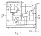
- an output buffer circuit 4A includes, in addition to the transistors P1 and N6 of the output buffer circuit 4 of the first embodiment, an NPN transistor Q1 having a collector connected to the power source VDD, a base connected to the source of the transistor P1 and an emitter connected to the output terminal TO and a buffer circuit 8 having an input connected to the input terminal TI and an output connected to the base of the transistor Q1 and the source of the transistor P1.
- the transfer gate 6 since the transfer gate 6 is still in the conduction state, the low level output of the inverter 1 is supplied to the gate of the transistor P1 to turn the latter ON. Simultaneously, the transistor P2 is turned ON to maintain the transfer gate 6 in the conduction state. Therefore, the level of the output terminal TO is changed from L to H. However, since a forward voltage is supplied between the base and the emitter of the transistor Q1 by the transistor P1 in ON state, the transistor Q1 is turned ON at very high speed. Further, due to the transistor P1 in ON state, the output level of the output terminal TO which is dropped by the forward voltage of the transistor Q1 is pushed up to the source voltage VDD.
- a load driving element connected to the output terminal TO is the NPN transistor Q1
- the smaller the ON resistance of the transistor P1 is better it is possible to make the element size of the transistor P1 small. Therefore, it is possible to make the sizes of the transistors N8 and P5 of the transfer gate 6 for driving the transistor P1 and the inverter 1 small. Thus, it is possible to reduce an area occupied by the elements constituting the output circuit and to reduce the power consumption of the output circuit.
- Fig. 3(A) shows simulation waveforms of the ground current when VPP greater than VDD (3V) is supplied to TO.
- the curve A stands for the prior art circuit and the curve B stands for the first and second embodiment of this invention, respectively.
- the current consumption increases proportionally to VPP.
- the current consumption of this invention circuit is substantially zero.
- Fig. 3(B) shows output voltage waveforms of the first and second embodiment of this invention.
- the curves A, B and C stand for input voltage, the first embodiment and the second embodiment, respectively.
- the curve C improves a delay time by about 46% with respect to the curve B.
- the output circuit of the present invention which includes a transfer gate for supplying a control signal corresponding to an input signal to an output transistor and a protection control circuit for closing the transfer gate when an over-voltage is applied to an output terminal can prevent a current from flowing into a power source thereof as well as its ground when the over-voltage is applied to the output terminal. Therefore, it is possible to substantially reduce power consumption and substantially reduce a junction temperature of each of elements constituting an integrated circuit.
Landscapes
- Physics & Mathematics (AREA)
- Engineering & Computer Science (AREA)
- Computer Hardware Design (AREA)
- Computing Systems (AREA)
- General Engineering & Computer Science (AREA)
- Mathematical Physics (AREA)
- Logic Circuits (AREA)
- Semiconductor Integrated Circuits (AREA)
- Metal-Oxide And Bipolar Metal-Oxide Semiconductor Integrated Circuits (AREA)
- Bipolar Integrated Circuits (AREA)
- Electronic Switches (AREA)
Applications Claiming Priority (3)
| Application Number | Priority Date | Filing Date | Title |
|---|---|---|---|
| JP266936/95 | 1995-10-16 | ||
| JP26693695 | 1995-10-16 | ||
| JP7266936A JP2959449B2 (ja) | 1995-10-16 | 1995-10-16 | 出力回路 |
Publications (2)
| Publication Number | Publication Date |
|---|---|
| EP0768762A1 true EP0768762A1 (de) | 1997-04-16 |
| EP0768762B1 EP0768762B1 (de) | 2001-12-19 |
Family
ID=17437750
Family Applications (1)
| Application Number | Title | Priority Date | Filing Date |
|---|---|---|---|
| EP96116613A Expired - Lifetime EP0768762B1 (de) | 1995-10-16 | 1996-10-16 | Ausgangsschaltung |
Country Status (4)
| Country | Link |
|---|---|
| US (1) | US5864245A (de) |
| EP (1) | EP0768762B1 (de) |
| JP (1) | JP2959449B2 (de) |
| DE (1) | DE69618135T2 (de) |
Cited By (2)
| Publication number | Priority date | Publication date | Assignee | Title |
|---|---|---|---|---|
| EP0807334A1 (de) * | 1995-12-01 | 1997-11-19 | Koninklijke Philips Electronics N.V. | Schaltung mit busleitung und busschnittstelle |
| EP0964519A3 (de) * | 1998-06-12 | 2000-10-11 | Nec Corporation | Integrierte logische Halbleiterschaltung mit sequentiellen Schaltungen zur Unterdrückung von Subschwellenwert-Leckstrom |
Families Citing this family (11)
| Publication number | Priority date | Publication date | Assignee | Title |
|---|---|---|---|---|
| US6066963A (en) * | 1997-09-29 | 2000-05-23 | Cypress Semiconductor Corp | MOS output driver, and circuit and method of controlling same |
| US6097237A (en) * | 1998-01-29 | 2000-08-01 | Sun Microsystems, Inc. | Overshoot/undershoot protection scheme for low voltage output buffer |
| US6417696B1 (en) * | 1999-12-20 | 2002-07-09 | Cypress Semiconductor Corp. | Interface circuit for mixed voltage I/O buffer to provide gate oxide protection |
| US6344958B1 (en) * | 2000-02-10 | 2002-02-05 | Fairchild Semiconductor Corp. | Overvoltage protection circuit with overvoltage removal sensing |
| US6208178B1 (en) | 2000-02-23 | 2001-03-27 | Pericom Semiconductor Corp. | CMOS over voltage-tolerant output buffer without transmission gate |
| US6329835B1 (en) | 2000-02-23 | 2001-12-11 | Pericom Semiconductor Corp. | Quiet output buffers with neighbor sensing of wide bus and control signals |
| US6317000B1 (en) | 2000-10-05 | 2001-11-13 | Texas Instruments Incorporated | Overload recovery circuit and method |
| US6724594B2 (en) * | 2000-12-20 | 2004-04-20 | National Semiconductor Corporation | Over voltage protection test multiplexer and methods of operating the same |
| US6703900B2 (en) | 2002-06-05 | 2004-03-09 | Texas Instruments Incorporated | Fast, stable overload recovery circuit and method |
| JP6648895B2 (ja) * | 2015-09-17 | 2020-02-14 | 新日本無線株式会社 | 出力回路 |
| JP2024123621A (ja) * | 2023-03-01 | 2024-09-12 | ルネサスエレクトロニクス株式会社 | 過電圧保護回路、コネクタ及び半導体装置 |
Citations (2)
| Publication number | Priority date | Publication date | Assignee | Title |
|---|---|---|---|---|
| EP0630109A2 (de) * | 1993-06-18 | 1994-12-21 | Texas Instruments Incorporated | Treiberschaltung mit niedriger Ausgangspannung |
| US5444397A (en) * | 1994-10-05 | 1995-08-22 | Pericom Semiconductor Corp. | All-CMOS high-impedance output buffer for a bus driven by multiple power-supply voltages |
Family Cites Families (5)
| Publication number | Priority date | Publication date | Assignee | Title |
|---|---|---|---|---|
| US5004936A (en) * | 1989-03-31 | 1991-04-02 | Texas Instruments Incorporated | Non-loading output driver circuit |
| US5151619A (en) * | 1990-10-11 | 1992-09-29 | International Business Machines Corporation | Cmos off chip driver circuit |
| GB2258100B (en) * | 1991-06-28 | 1995-02-15 | Digital Equipment Corp | Floating-well CMOS output driver |
| US5406140A (en) * | 1993-06-07 | 1995-04-11 | National Semiconductor Corporation | Voltage translation and overvoltage protection |
| JP3311133B2 (ja) * | 1994-02-16 | 2002-08-05 | 株式会社東芝 | 出力回路 |
-
1995
- 1995-10-16 JP JP7266936A patent/JP2959449B2/ja not_active Expired - Fee Related
-
1996
- 1996-10-15 US US08/730,603 patent/US5864245A/en not_active Expired - Lifetime
- 1996-10-16 EP EP96116613A patent/EP0768762B1/de not_active Expired - Lifetime
- 1996-10-16 DE DE69618135T patent/DE69618135T2/de not_active Expired - Lifetime
Patent Citations (2)
| Publication number | Priority date | Publication date | Assignee | Title |
|---|---|---|---|---|
| EP0630109A2 (de) * | 1993-06-18 | 1994-12-21 | Texas Instruments Incorporated | Treiberschaltung mit niedriger Ausgangspannung |
| US5444397A (en) * | 1994-10-05 | 1995-08-22 | Pericom Semiconductor Corp. | All-CMOS high-impedance output buffer for a bus driven by multiple power-supply voltages |
Cited By (3)
| Publication number | Priority date | Publication date | Assignee | Title |
|---|---|---|---|---|
| EP0807334A1 (de) * | 1995-12-01 | 1997-11-19 | Koninklijke Philips Electronics N.V. | Schaltung mit busleitung und busschnittstelle |
| EP0964519A3 (de) * | 1998-06-12 | 2000-10-11 | Nec Corporation | Integrierte logische Halbleiterschaltung mit sequentiellen Schaltungen zur Unterdrückung von Subschwellenwert-Leckstrom |
| US6246265B1 (en) | 1998-06-12 | 2001-06-12 | Nec Corporation | Semiconductor integrated logic circuit with sequential circuits capable of preventing subthreshold leakage current |
Also Published As
| Publication number | Publication date |
|---|---|
| EP0768762B1 (de) | 2001-12-19 |
| US5864245A (en) | 1999-01-26 |
| JP2959449B2 (ja) | 1999-10-06 |
| DE69618135D1 (de) | 2002-01-31 |
| DE69618135T2 (de) | 2002-08-29 |
| JPH09116415A (ja) | 1997-05-02 |
Similar Documents
| Publication | Publication Date | Title |
|---|---|---|
| EP0621694B1 (de) | Schnittstellenschaltung mit niedrigem Verbrauch | |
| EP0329285B1 (de) | Ausgangspuffer | |
| EP0282702B1 (de) | BIFET-Logik-Schaltung | |
| US6040729A (en) | Digital output buffer for multiple voltage system | |
| KR100194904B1 (ko) | 바이폴라 트랜지스터와 mos 트랜지스터의 복합회로 및 그것을 사용한 반도체 집적회로 장치 | |
| US4678940A (en) | TTL compatible merged bipolar/CMOS output buffer circuits | |
| KR20010049227A (ko) | 레벨조정회로 및 이를 포함하는 데이터 출력회로 | |
| CN111313878B (zh) | 一种模拟开关电路 | |
| US5864245A (en) | Output circuit with overvoltage protection | |
| EP0351820B1 (de) | Ausgangschaltung | |
| JPH0693615B2 (ja) | ドライバ回路 | |
| US5469097A (en) | Translator circuit with symmetrical switching delays | |
| JPH0252460B2 (de) | ||
| US5038058A (en) | BiCMOS TTL output driver | |
| US5095229A (en) | Full-swing bicmos driver | |
| KR930007566B1 (ko) | Bi-CMOS회로 | |
| US5118972A (en) | BiCMOS gate pull-down circuit | |
| JPH0677804A (ja) | 出力回路 | |
| KR0165986B1 (ko) | BiCMOS 논리 회로 | |
| US5077492A (en) | Bicmos circuitry having a combination cmos gate and a bipolar transistor | |
| JP2621248B2 (ja) | 半導体集積回路装置 | |
| KR950000352B1 (ko) | 반도체 논리회로 | |
| JPH03123220A (ja) | 出力回路 | |
| JPH06196996A (ja) | 出力バッファ回路 | |
| US20020005733A1 (en) | Switching circuit |
Legal Events
| Date | Code | Title | Description |
|---|---|---|---|
| PUAI | Public reference made under article 153(3) epc to a published international application that has entered the european phase |
Free format text: ORIGINAL CODE: 0009012 |
|
| 17P | Request for examination filed |
Effective date: 19970122 |
|
| AK | Designated contracting states |
Kind code of ref document: A1 Designated state(s): DE FR GB |
|
| 17Q | First examination report despatched |
Effective date: 19991013 |
|
| GRAG | Despatch of communication of intention to grant |
Free format text: ORIGINAL CODE: EPIDOS AGRA |
|
| GRAG | Despatch of communication of intention to grant |
Free format text: ORIGINAL CODE: EPIDOS AGRA |
|
| GRAH | Despatch of communication of intention to grant a patent |
Free format text: ORIGINAL CODE: EPIDOS IGRA |
|
| GRAH | Despatch of communication of intention to grant a patent |
Free format text: ORIGINAL CODE: EPIDOS IGRA |
|
| GRAA | (expected) grant |
Free format text: ORIGINAL CODE: 0009210 |
|
| AK | Designated contracting states |
Kind code of ref document: B1 Designated state(s): DE FR GB |
|
| REG | Reference to a national code |
Ref country code: GB Ref legal event code: IF02 |
|
| REF | Corresponds to: |
Ref document number: 69618135 Country of ref document: DE Date of ref document: 20020131 |
|
| ET | Fr: translation filed | ||
| PLBE | No opposition filed within time limit |
Free format text: ORIGINAL CODE: 0009261 |
|
| STAA | Information on the status of an ep patent application or granted ep patent |
Free format text: STATUS: NO OPPOSITION FILED WITHIN TIME LIMIT |
|
| 26N | No opposition filed | ||
| REG | Reference to a national code |
Ref country code: GB Ref legal event code: 732E |
|
| REG | Reference to a national code |
Ref country code: FR Ref legal event code: TP |
|
| PGFP | Annual fee paid to national office [announced via postgrant information from national office to epo] |
Ref country code: FR Payment date: 20081014 Year of fee payment: 13 |
|
| PGFP | Annual fee paid to national office [announced via postgrant information from national office to epo] |
Ref country code: GB Payment date: 20081015 Year of fee payment: 13 |
|
| REG | Reference to a national code |
Ref country code: FR Ref legal event code: ST Effective date: 20100630 |
|
| PG25 | Lapsed in a contracting state [announced via postgrant information from national office to epo] |
Ref country code: FR Free format text: LAPSE BECAUSE OF NON-PAYMENT OF DUE FEES Effective date: 20091102 |
|
| PG25 | Lapsed in a contracting state [announced via postgrant information from national office to epo] |
Ref country code: GB Free format text: LAPSE BECAUSE OF NON-PAYMENT OF DUE FEES Effective date: 20091016 |
|
| REG | Reference to a national code |
Ref country code: DE Ref legal event code: R082 Ref document number: 69618135 Country of ref document: DE Representative=s name: GLAWE DELFS MOLL - PARTNERSCHAFT VON PATENT- U, DE |
|
| REG | Reference to a national code |
Ref country code: DE Ref legal event code: R082 Ref document number: 69618135 Country of ref document: DE Representative=s name: GLAWE DELFS MOLL PARTNERSCHAFT MBB VON PATENT-, DE Effective date: 20120828 Ref country code: DE Ref legal event code: R082 Ref document number: 69618135 Country of ref document: DE Representative=s name: GLAWE DELFS MOLL - PARTNERSCHAFT VON PATENT- U, DE Effective date: 20120828 Ref country code: DE Ref legal event code: R081 Ref document number: 69618135 Country of ref document: DE Owner name: RENESAS ELECTRONICS CORPORATION, KAWASAKI-SHI, JP Free format text: FORMER OWNER: NEC ELECTRONICS CORP., KAWASAKI, KANAGAWA, JP Effective date: 20120828 Ref country code: DE Ref legal event code: R081 Ref document number: 69618135 Country of ref document: DE Owner name: RENESAS ELECTRONICS CORPORATION, JP Free format text: FORMER OWNER: NEC ELECTRONICS CORP., KAWASAKI, JP Effective date: 20120828 |
|
| PGFP | Annual fee paid to national office [announced via postgrant information from national office to epo] |
Ref country code: DE Payment date: 20130227 Year of fee payment: 17 |
|
| REG | Reference to a national code |
Ref country code: DE Ref legal event code: R119 Ref document number: 69618135 Country of ref document: DE Effective date: 20140501 |
|
| PG25 | Lapsed in a contracting state [announced via postgrant information from national office to epo] |
Ref country code: DE Free format text: LAPSE BECAUSE OF NON-PAYMENT OF DUE FEES Effective date: 20140501 |