EP0769872A2 - Circuit avec un étage de réception haute fréquence et un étage de transmission - Google Patents
Circuit avec un étage de réception haute fréquence et un étage de transmission Download PDFInfo
- Publication number
- EP0769872A2 EP0769872A2 EP96202842A EP96202842A EP0769872A2 EP 0769872 A2 EP0769872 A2 EP 0769872A2 EP 96202842 A EP96202842 A EP 96202842A EP 96202842 A EP96202842 A EP 96202842A EP 0769872 A2 EP0769872 A2 EP 0769872A2
- Authority
- EP
- European Patent Office
- Prior art keywords
- frequency
- stage
- signal
- tuner
- modulator
- Prior art date
- Legal status (The legal status is an assumption and is not a legal conclusion. Google has not performed a legal analysis and makes no representation as to the accuracy of the status listed.)
- Granted
Links
- 230000005540 biological transmission Effects 0.000 title claims abstract description 20
- 230000010355 oscillation Effects 0.000 claims abstract description 25
- 230000003321 amplification Effects 0.000 claims abstract description 6
- 239000013078 crystal Substances 0.000 claims abstract description 6
- 238000003199 nucleic acid amplification method Methods 0.000 claims abstract description 6
- 239000010453 quartz Substances 0.000 claims abstract description 3
- VYPSYNLAJGMNEJ-UHFFFAOYSA-N silicon dioxide Inorganic materials O=[Si]=O VYPSYNLAJGMNEJ-UHFFFAOYSA-N 0.000 claims abstract description 3
- 238000010276 construction Methods 0.000 abstract description 2
- 238000004519 manufacturing process Methods 0.000 abstract description 2
- 230000005236 sound signal Effects 0.000 description 7
- 230000008878 coupling Effects 0.000 description 2
- 238000010168 coupling process Methods 0.000 description 2
- 238000005859 coupling reaction Methods 0.000 description 2
- 230000006978 adaptation Effects 0.000 description 1
- 230000000712 assembly Effects 0.000 description 1
- 238000000429 assembly Methods 0.000 description 1
- 230000010354 integration Effects 0.000 description 1
- 239000004065 semiconductor Substances 0.000 description 1
Images

Classifications
-
- H—ELECTRICITY
- H03—ELECTRONIC CIRCUITRY
- H03J—TUNING RESONANT CIRCUITS; SELECTING RESONANT CIRCUITS
- H03J3/00—Continuous tuning
-
- H—ELECTRICITY
- H03—ELECTRONIC CIRCUITRY
- H03L—AUTOMATIC CONTROL, STARTING, SYNCHRONISATION OR STABILISATION OF GENERATORS OF ELECTRONIC OSCILLATIONS OR PULSES
- H03L7/00—Automatic control of frequency or phase; Synchronisation
- H03L7/06—Automatic control of frequency or phase; Synchronisation using a reference signal applied to a frequency- or phase-locked loop
- H03L7/08—Details of the phase-locked loop
- H03L7/0805—Details of the phase-locked loop the loop being adapted to provide an additional control signal for use outside the loop
-
- H—ELECTRICITY
- H03—ELECTRONIC CIRCUITRY
- H03J—TUNING RESONANT CIRCUITS; SELECTING RESONANT CIRCUITS
- H03J5/00—Discontinuous tuning; Selecting predetermined frequencies; Selecting frequency bands with or without continuous tuning in one or more of the bands, e.g. push-button tuning, turret tuner
- H03J5/02—Discontinuous tuning; Selecting predetermined frequencies; Selecting frequency bands with or without continuous tuning in one or more of the bands, e.g. push-button tuning, turret tuner with variable tuning element having a number of predetermined settings and adjustable to a desired one of these settings
- H03J5/0245—Discontinuous tuning using an electrical variable impedance element, e.g. a voltage variable reactive diode, in which no corresponding analogue value either exists or is preset, i.e. the tuning information is only available in a digital form
- H03J5/0272—Discontinuous tuning using an electrical variable impedance element, e.g. a voltage variable reactive diode, in which no corresponding analogue value either exists or is preset, i.e. the tuning information is only available in a digital form the digital values being used to preset a counter or a frequency divider in a phase locked loop, e.g. frequency synthesizer
-
- H—ELECTRICITY
- H03—ELECTRONIC CIRCUITRY
- H03J—TUNING RESONANT CIRCUITS; SELECTING RESONANT CIRCUITS
- H03J5/00—Discontinuous tuning; Selecting predetermined frequencies; Selecting frequency bands with or without continuous tuning in one or more of the bands, e.g. push-button tuning, turret tuner
- H03J5/24—Discontinuous tuning; Selecting predetermined frequencies; Selecting frequency bands with or without continuous tuning in one or more of the bands, e.g. push-button tuning, turret tuner with a number of separate pretuned tuning circuits or separate tuning elements selectively brought into circuit, e.g. for waveband selection or for television channel selection
- H03J5/242—Discontinuous tuning; Selecting predetermined frequencies; Selecting frequency bands with or without continuous tuning in one or more of the bands, e.g. push-button tuning, turret tuner with a number of separate pretuned tuning circuits or separate tuning elements selectively brought into circuit, e.g. for waveband selection or for television channel selection used exclusively for band selection
- H03J5/244—Discontinuous tuning; Selecting predetermined frequencies; Selecting frequency bands with or without continuous tuning in one or more of the bands, e.g. push-button tuning, turret tuner with a number of separate pretuned tuning circuits or separate tuning elements selectively brought into circuit, e.g. for waveband selection or for television channel selection used exclusively for band selection using electronic means
-
- H—ELECTRICITY
- H04—ELECTRIC COMMUNICATION TECHNIQUE
- H04N—PICTORIAL COMMUNICATION, e.g. TELEVISION
- H04N5/00—Details of television systems
- H04N5/44—Receiver circuitry for the reception of television signals according to analogue transmission standards
-
- H—ELECTRICITY
- H04—ELECTRIC COMMUNICATION TECHNIQUE
- H04N—PICTORIAL COMMUNICATION, e.g. TELEVISION
- H04N7/00—Television systems
- H04N7/20—Adaptations for transmission via a GHz frequency band, e.g. via satellite
Definitions
- the invention relates to a circuit arrangement with a high-frequency receiver stage (tuner) and a transmission stage (splitter) and a modulation arrangement (modulator) comprising transmission stage (splitter-modulator), the signal division circuit (splitter) having a high-frequency signal input for supplying a high-frequency input signal, a High-frequency signal output for outputting a high-frequency output signal, a first line for outputting the high-frequency input signal to the receiving stage (tuner) and a second line for supplying a high-frequency output signal from the modulation arrangement (modulator), and wherein the reception stage (tuner) for demodulating the high-frequency input signal and the modulation arrangement (modulator ) is set up for converting a baseband signal into the high-frequency output signal to be emitted by it, with devices for generating reference oscillations for the high-frequency reception stage (tuner) and the transmission stage (splitter modulator), these devices locking a common quartz crystal for the radio frequency reception stage (
- Such a circuit arrangement is described in European patent application 95 200 961.1.
- a low circuit outlay is sought for a circuit arrangement which comprises both a tuner and a splitter modulator. It is stated as a particularly low-cost arrangement that only one for both the modulation arrangement in the signal splitting circuit and for the high-frequency reception stage only vibration generator with a single oscillator stage is used.
- the object of the invention is to achieve as compact a construction as possible by using as few components as possible and, on the other hand, the lowest possible manufacturing costs in a circuit arrangement of the aforementioned type.
- the radio-frequency receiving stage comprises at least one signal processing branch for frequency-selective receiver, amplification and / or frequency mixing of the radio-frequency signals in each frequency range (band) and the devices for generating Reference oscillations (oscillation generator) for each signal processing branch comprises a separate oscillator stage, one of these oscillator stages also being used to generate the reference oscillation for the transmission stage (splitter modulator).
- a separate oscillator stage is therefore used for each frequency range in each associated signal processing branch. This can be optimally adapted to the filter stages of this signal processing branch. This avoids a very complex adaptation of a single oscillator stage to filter stages of different signal processing branches for different frequency ranges.
- oscillator stages are also used for the modulation arrangement in order to deliver a carrier oscillation required for this.
- the modulation arrangement in the case of several signal processing branches, several frequency ranges in the high-frequency reception stage - can be connected to the suitable oscillator stage.
- the operation of the circuit arrangement is particularly simple in that either only the high-frequency receiving stage or only the modulation arrangement is operated; however, the invention also enables simultaneous operation.
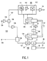
- a high-frequency input signal for example a television signal from an antenna, can be fed to the splitter 103 via a high-frequency signal input 104. It reaches a first signal switch 106 via a first preamplifier 105 and from it to a first line 107 on the one hand and to a second signal switch 109 via a second preamplifier 108, respectively. From this it can be emitted via a high-frequency signal output 110.
- the high-frequency input signal reaches the tuner 101 from the first line 107, in which a frequency selection 111, an amplitude control 112 and a downmixing 113 are carried out in the usual way by stages customary for this.
- An intermediate frequency signal is emitted via an output amplifier 114.
- the stages 111 for the frequency selection and 113 for the downmixing are supplied in a conventional manner with reference oscillations from an oscillation generator assigned to the tuner 101, which comprises a phase-locked loop 115 and an oscillator stage 116.
- the phase-locked loop 115 can be controlled to tune the tuner 101 via control lines 117, preferably an I2C bus.
- the modulator 102 contains, in a manner known per se, an audio signal modulation stage 33, to which an audio baseband signal can be fed at an audio signal input 32 and which modulates it onto a sound carrier oscillation.
- the modulated audio signal is superimposed in a low-frequency signal superposition stage 31 on a baseband video signal supplied via an input 30.
- the FBAS signal thus obtained is modulated in a modulation stage 35 onto a high-frequency carrier oscillation, which is generated in a vibration generator of the modulator 102, which comprises a second phase-locked loop 123 and a second oscillator stage 124.
- the vibration generator 123, 124 of the modulator 102 has the same structure as that of the tuner 101.
- both oscillation generators 115, 116 and 123, 124 are controlled from a single crystal oscillator, wherein a transistor coupling stage 126 for oscillation amplification and low-resistance coupling can be arranged between the crystal oscillator 22 and the second phase-locked loop 123.
- a second line 127 feeds the high-frequency output signal of the modulator 102 to the second signal switch 109 of the splitter 103, via which it reaches the high-frequency signal output 110.
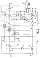
- the embodiment of FIG. 2 comprises a broadband input amplifier 1, which is connected on the input side to an input 2 for the high-frequency signals and on the output side to a switching stage 3, and three signal processing branches adjoining the switching stage 3 with a final signal combination.
- Each of the signal processing branches in FIG. 2 comprises filter stages 4, 5 and 6, which are connected to the switchover stage 3, a controllable amplifier stage 7, 8 and 9 each following the filter stages 4, 5 and 6 as well as a mixer stage 10 , 11 or 12 following the associated controllable amplifier stage 7, 8 or 9. From input 2 for the high-frequency signals, these are optionally supplied to one of the signal processing branches via the broadband input amplifier and the switching stage 3.
- the desired frequency band assigned to the signal processing branch is selected in filter stages 4, 5 and 6.
- the mixing stages 10, 11 and 12 are then supplied with the high-frequency signals exclusively of the filtered frequency band and their frequencies are mixed down in the mixing stages 10, 11 and 12.
- the signal combination formed in the arrangement according to FIG. 2 by a line node 13 and an output amplifier 14, enables the down-mixed high-frequency signals to be fed to a common output 15.
- the signal combination can also comprise only the line node;
- the output amplifier 14 then already belongs together with the output 15 to an output branch common to all signal processing branches.
- a common vibration generator is used to generate the vibrations required for mixing down the high-frequency signals, which comprises a phase-locked loop 16 common to all signal processing branches and a separate oscillator stage 17, 18 and 19 for each of the signal processing branches.
- the phase locked loop 16 and the oscillator stages 17, 18 and 19 are connected to one another in a manner known per se.
- the oscillator stages 17, 18, 19 can be switched on or off via a data line 20, so that only the oscillator stages 17, 18 and 19 emit an oscillation, the signal processing branch of which via the switching stage 3 is connected to input 2 (via input amplifier 1).
- the data line 20 can then also be routed to the switching stage 3 in the same way.
- the frequency of the oscillation emitted by the oscillation generator 16 to 19 can be set via a data input 21 of the phase-locked loop 16.
- the oscillation generator 16 to 19 is also connected to a crystal oscillator 22 as a frequency reference.
- the controllable amplifier stages 7, 8, 9 have a control input 23 via which the gain factor of the amplifier stages 7, 8, 9 can be set.
- the controllable amplifier stages 7, 8, 9 can then be integrated into a control loop for amplitude control or power control of the high-frequency signals.
- the data line 20 and the data input 21 of the phase-locked loop 16 can be connected to a controller (not shown) for the reception operation of the high-frequency reception stage.
- the filter stages 4, 5, 6 are connected via a line 24 of the phase-locked loop 16. Signals for frequency selection from the oscillation generator 16 to 19 can be supplied via this line 24 in a conventional manner.
- tuning diodes present in filter stages 4, 5, 6 are given the same tuning as oscillator stages 17, 18, 19.
- FIG. 2 also shows the integration of the embodiment of the high-frequency reception stage described above in high-frequency signal processing of a video recorder.
- 2 shows a further input amplifier stage 25, which is connected on the input side to an antenna input 26 of the video recorder and on the output side to input 2 of the high-frequency reception stage for the high-frequency signals.
- the input 2 is also connected via a loop-through amplifier 27 to an input of a high-frequency signal superposition stage 28. Its output forms an antenna output 29 of the video recorder.
- An input 30 for the baseband video signal forms a first input of a low-frequency signal superimposition stage 31.
- An input 32 for an audio signal is led to an audio signal modulation stage 33. This is connected to a second input of the low-frequency signal superposition stage 31.
- the audio signal supplied from the input 32 is modulated onto an auxiliary carrier oscillation and then, in the low-frequency signal superposition stage 31, is additively superimposed on the baseband video signal from the input 30. In this way, a CVBS signal is generated and output via an output 34 of the low-frequency superposition stage 31.
- the output 34 leads to a modulation stage 35, in which the CVBS signal is mixed up with an oscillation from one of the oscillator stages, here the oscillator stage 19 for the third signal processing branch.
- This produces a high-frequency signal, which is fed to the high-frequency signal superposition stage 28 for transmission to the antenna output 29 of the video recorder.
- the elements surrounded by the dashed line 36 are advantageously combined to form an integrated assembly.
- the elements surrounded by the dash-dotted line 37 can be combined to form a further integrated assembly.
- These integrated assemblies can in particular be integrated on a semiconductor body.
- Fig. 3 shows a second embodiment of the radio frequency receiving stage according to the invention.
- the broadband input amplifier 1 was replaced by a broadband controllable input amplifier 38, which is now connected to the control input 23 for the purpose of amplitude and power control of the high-frequency signals.
- the controllable amplifier stages 7, 8, 9 in the signal processing branches are omitted; 3, they can be replaced by amplifier stages with constant amplification factors if a further signal amplification or return loss is desired at these points in the circuit arrangement.
- tuner 101 comprises the elements identified by reference numerals 3 to 13 in FIGS. 2 and 3
- modulator 102 comprises elements 30 to 35
- splitter 103 preferably contains elements 1, 2, 25, 27 and 28 in the exemplary embodiments of FIGS. 2 and 3. Since the splitter according to FIG. 1 with the second signal switch 109, which corresponds in its function to the high-frequency signal superposition stage 28 in FIGS. 2 and 3, not only performs a signal splitting but also a signal summary, it can also be called a splitter combiner.
- the first signal switch 106 takes over the task of input 2 for the high-frequency signals.
- the high-frequency signal input 104 corresponds to the antenna input 26 of the video recorder, the first amplifier 105 to the further input amplifier stage 25, the second preamplifier 108 to the loop-through amplifier 27 and the high-frequency signal output 110 to the antenna output 29 of the video recorder.
- the frequency selection 111 in FIG. 1 is carried out in FIGS. 2 and 3 by the filter stages 4 to 6 and the amplitude control 112 by the controllable amplifier stages 7 to 9, the downward mixing 113 takes place in the mixing stages 10 to 12.
- data input 21 fulfills the function of control lines 117 from FIG. 1.
- a preferred application of the invention is in high-frequency processing stages of satellite reception systems and video recorders.
Landscapes
- Engineering & Computer Science (AREA)
- Signal Processing (AREA)
- Multimedia (AREA)
- Computer Hardware Design (AREA)
- General Physics & Mathematics (AREA)
- Astronomy & Astrophysics (AREA)
- Physics & Mathematics (AREA)
- Microelectronics & Electronic Packaging (AREA)
- Superheterodyne Receivers (AREA)
- Transmitters (AREA)
- Channel Selection Circuits, Automatic Tuning Circuits (AREA)
- Two-Way Televisions, Distribution Of Moving Picture Or The Like (AREA)
- Radio Relay Systems (AREA)
Applications Claiming Priority (2)
| Application Number | Priority Date | Filing Date | Title |
|---|---|---|---|
| DE19538544A DE19538544A1 (de) | 1995-10-17 | 1995-10-17 | Schaltungsanordnung mit einer Hochfrequenz-Empfangsstufe und einer Übertragungsstufe |
| DE19538544 | 1995-10-17 |
Publications (3)
| Publication Number | Publication Date |
|---|---|
| EP0769872A2 true EP0769872A2 (fr) | 1997-04-23 |
| EP0769872A3 EP0769872A3 (fr) | 1997-05-02 |
| EP0769872B1 EP0769872B1 (fr) | 2002-02-27 |
Family
ID=7775015
Family Applications (1)
| Application Number | Title | Priority Date | Filing Date |
|---|---|---|---|
| EP96202842A Expired - Lifetime EP0769872B1 (fr) | 1995-10-17 | 1996-10-11 | Circuit avec un étage de réception haute fréquence et un étage de transmission |
Country Status (6)
| Country | Link |
|---|---|
| US (1) | US5867771A (fr) |
| EP (1) | EP0769872B1 (fr) |
| JP (1) | JP3816995B2 (fr) |
| KR (1) | KR100441183B1 (fr) |
| DE (2) | DE19538544A1 (fr) |
| SG (1) | SG55235A1 (fr) |
Families Citing this family (10)
| Publication number | Priority date | Publication date | Assignee | Title |
|---|---|---|---|---|
| US6442382B1 (en) * | 1997-06-27 | 2002-08-27 | Agere Systems Guardian Corp. | Filter switching system and method |
| DE19728315A1 (de) * | 1997-07-03 | 1999-01-07 | Philips Patentverwaltung | Fernsehsignal-Empfänger |
| US6405025B1 (en) * | 1997-12-09 | 2002-06-11 | Nokia Mobile Phones Limited | Method for selecting the frequency range in radio communication devices operating in several frequency ranges and a radio communication device |
| JP2002118795A (ja) * | 2000-10-05 | 2002-04-19 | Alps Electric Co Ltd | テレビジョン信号受信チューナー |
| JP3719926B2 (ja) * | 2000-11-14 | 2005-11-24 | シャープ株式会社 | デジタル信号受信用チューナ |
| GB0122983D0 (en) * | 2001-09-25 | 2001-11-14 | Zarlink Semiconductor Ltd | Rdio fequency tuner front end and tuner |
| US7024220B2 (en) * | 2001-10-09 | 2006-04-04 | Kyocera Wireless Corp. | GPS receiver system and method |
| DE10163798A1 (de) * | 2001-12-22 | 2003-07-03 | Philips Intellectual Property | Fernsehsignal-Empfänger mit universalem Ausgang für verschiedenartige Oberflächenwellenfilter |
| CN100506174C (zh) * | 2002-09-20 | 2009-07-01 | 医疗器械创新有限公司 | 具有可伸缩护套的外科手术刀 |
| US8750441B2 (en) * | 2010-12-20 | 2014-06-10 | Texas Instruments Incorporated | Signal cancellation to reduce phase noise, period jitter, and other contamination in local oscillator, frequency timing, or other timing generators or signal sources |
Family Cites Families (10)
| Publication number | Priority date | Publication date | Assignee | Title |
|---|---|---|---|---|
| US4157505A (en) * | 1977-06-13 | 1979-06-05 | Regency Electronics | Plural band scanning radio with direct switch of RF amplifying transistors |
| US4379271A (en) * | 1980-08-25 | 1983-04-05 | Rca Corporation | Input selection arrangement for applying different local oscillator signals to a prescaler of a phase-lock loop tuning system |
| US4667243A (en) * | 1985-10-31 | 1987-05-19 | Rca Corporation | Television receiver for direct broadcast satellite signals |
| US4894720A (en) * | 1987-07-31 | 1990-01-16 | Sanyo Electric Co., Ltd. | Circuit for selectively outputting high frequency signals |
| DE3728381A1 (de) * | 1987-08-26 | 1989-03-09 | Thomson Brandt Gmbh | Schaltungsanordnung zur verteilung eines antennensignals |
| DE3821714A1 (de) * | 1988-06-28 | 1990-01-04 | Telefunken Electronic Gmbh | Fernsehtuner |
| US5420646A (en) * | 1991-12-30 | 1995-05-30 | Zenith Electronics Corp. | Bandswitched tuning system having a plurality of local oscillators for a digital television receiver |
| EP0678981A3 (fr) * | 1994-04-21 | 1996-05-15 | Philips Patentverwaltung | Etage de réception à haute fréquence. |
| DE19509567A1 (de) * | 1994-04-21 | 1995-10-26 | Philips Patentverwaltung | Hochfrequenz-Empfangsstufe |
| US5758266A (en) * | 1994-09-30 | 1998-05-26 | Qualcomm Incorporated | Multiple frequency communication device |
-
1995
- 1995-10-17 DE DE19538544A patent/DE19538544A1/de not_active Withdrawn
-
1996
- 1996-10-11 EP EP96202842A patent/EP0769872B1/fr not_active Expired - Lifetime
- 1996-10-11 DE DE59608783T patent/DE59608783D1/de not_active Expired - Lifetime
- 1996-10-16 JP JP27338696A patent/JP3816995B2/ja not_active Expired - Fee Related
- 1996-10-16 SG SG1996010870A patent/SG55235A1/en unknown
- 1996-10-17 US US08/733,307 patent/US5867771A/en not_active Expired - Lifetime
- 1996-10-17 KR KR1019960046394A patent/KR100441183B1/ko not_active Expired - Fee Related
Also Published As
| Publication number | Publication date |
|---|---|
| KR100441183B1 (ko) | 2004-10-08 |
| KR970024552A (ko) | 1997-05-30 |
| SG55235A1 (en) | 1999-07-20 |
| DE19538544A1 (de) | 1997-04-24 |
| JPH09135152A (ja) | 1997-05-20 |
| DE59608783D1 (de) | 2002-04-04 |
| US5867771A (en) | 1999-02-02 |
| EP0769872A3 (fr) | 1997-05-02 |
| JP3816995B2 (ja) | 2006-08-30 |
| EP0769872B1 (fr) | 2002-02-27 |
Similar Documents
| Publication | Publication Date | Title |
|---|---|---|
| EP0438075B1 (fr) | Système optique de transmission de télévision par câble | |
| DE69832620T2 (de) | Empfänger mit mehreren Tunern | |
| DE69005905T2 (de) | Empfänger für terrestrische AM- und Satelliten-FM-Fernsehsignale. | |
| DE3913593A1 (de) | Schaltungsanordnung zur umsetzung eines empfangenen modulierten informationssignals in ein zwischenfrequenzsignal | |
| DE69935173T2 (de) | Im Passband arbeitender, integrierter Mehrmoden-sigma-delta-Empfänger mit Interferenzverringerung und Verfahren zur dessen Anwendung | |
| DE19639237C2 (de) | Doppel-Fernsehtuner | |
| DE69637274T2 (de) | TDMA-Funkgerätschaltung mit variablem zweiten Lokaloszillator | |
| DE3855278T2 (de) | Rundfunkempfänger mit breitbandigem automatischem Verstärkungsregler | |
| DE3913520A1 (de) | Optisches kabelfernsehuebertragungssystem | |
| DE60002642T2 (de) | UHF-Filter mit vier Stufen die über eine gemeinsame Steuerspannung einstellbar sind | |
| DE69032520T2 (de) | RF-Modulator | |
| DE3903262C2 (fr) | ||
| EP0769872B1 (fr) | Circuit avec un étage de réception haute fréquence et un étage de transmission | |
| DE69024888T2 (de) | Durch Mikrokomputer gesteuerter Funkempfänger mit Synthesizer | |
| DE69530435T2 (de) | Demodulationsanordnung für einen hochauflösenden Fernsehempfänger | |
| DE69801358T2 (de) | Frequenzwandlerschaltung für Kabelempfänger mit Modem | |
| EP0679024B1 (fr) | Circuit avec un étage de réception haute fréquence et un modulateur pour transmission | |
| DE69918606T2 (de) | Direktrundfunkübertragungssatellitenempfänger | |
| DE3021216A1 (de) | Relaissender-empfaenger, insbesondere fuer am-duplexbetrieb | |
| DE19727718B4 (de) | Hochfrequenzeinrichtung mit Hochfrequenzmodulator und Fernseh-Tuner | |
| DE69328484T2 (de) | Regelkreis mit negativer Rückkopplung mit einer gemeinsamen Leitung für Eingang und Ausgang | |
| DE69535414T2 (de) | Frequenzmodulationsschaltung | |
| EP1592140B1 (fr) | Dispositif pour la réception de signaux de radiodiffusion | |
| EP0678981A2 (fr) | Etage de réception à haute fréquence | |
| EP0769850B1 (fr) | Etage d'entrée haute fréquence |
Legal Events
| Date | Code | Title | Description |
|---|---|---|---|
| PUAI | Public reference made under article 153(3) epc to a published international application that has entered the european phase |
Free format text: ORIGINAL CODE: 0009012 |
|
| PUAL | Search report despatched |
Free format text: ORIGINAL CODE: 0009013 |
|
| AK | Designated contracting states |
Kind code of ref document: A2 Designated state(s): DE FR GB |
|
| AK | Designated contracting states |
Kind code of ref document: A3 Designated state(s): DE FR GB |
|
| 17P | Request for examination filed |
Effective date: 19971103 |
|
| 17Q | First examination report despatched |
Effective date: 19991007 |
|
| RAP3 | Party data changed (applicant data changed or rights of an application transferred) |
Owner name: KONINKLIJKE PHILIPS ELECTRONICS N.V. Owner name: PHILIPS CORPORATE INTELLECTUAL PROPERTY GMBH |
|
| GRAG | Despatch of communication of intention to grant |
Free format text: ORIGINAL CODE: EPIDOS AGRA |
|
| GRAG | Despatch of communication of intention to grant |
Free format text: ORIGINAL CODE: EPIDOS AGRA |
|
| GRAH | Despatch of communication of intention to grant a patent |
Free format text: ORIGINAL CODE: EPIDOS IGRA |
|
| GRAH | Despatch of communication of intention to grant a patent |
Free format text: ORIGINAL CODE: EPIDOS IGRA |
|
| REG | Reference to a national code |
Ref country code: GB Ref legal event code: IF02 |
|
| GRAA | (expected) grant |
Free format text: ORIGINAL CODE: 0009210 |
|
| AK | Designated contracting states |
Kind code of ref document: B1 Designated state(s): DE FR GB |
|
| REF | Corresponds to: |
Ref document number: 59608783 Country of ref document: DE Date of ref document: 20020404 |
|
| GBT | Gb: translation of ep patent filed (gb section 77(6)(a)/1977) |
Effective date: 20020423 |
|
| ET | Fr: translation filed | ||
| RAP2 | Party data changed (patent owner data changed or rights of a patent transferred) |
Owner name: KONINKLIJKE PHILIPS ELECTRONICS N.V. Owner name: PHILIPS CORPORATE INTELLECTUAL PROPERTY GMBH |
|
| REG | Reference to a national code |
Ref country code: GB Ref legal event code: 746 Effective date: 20020912 |
|
| REG | Reference to a national code |
Ref country code: FR Ref legal event code: D6 |
|
| PLBE | No opposition filed within time limit |
Free format text: ORIGINAL CODE: 0009261 |
|
| STAA | Information on the status of an ep patent application or granted ep patent |
Free format text: STATUS: NO OPPOSITION FILED WITHIN TIME LIMIT |
|
| 26N | No opposition filed |
Effective date: 20021128 |
|
| REG | Reference to a national code |
Ref country code: GB Ref legal event code: 732E |
|
| REG | Reference to a national code |
Ref country code: FR Ref legal event code: TP |
|
| PGFP | Annual fee paid to national office [announced via postgrant information from national office to epo] |
Ref country code: DE Payment date: 20091008 Year of fee payment: 14 |
|
| PGFP | Annual fee paid to national office [announced via postgrant information from national office to epo] |
Ref country code: GB Payment date: 20091007 Year of fee payment: 14 Ref country code: FR Payment date: 20091102 Year of fee payment: 14 |
|
| GBPC | Gb: european patent ceased through non-payment of renewal fee |
Effective date: 20101011 |
|
| PG25 | Lapsed in a contracting state [announced via postgrant information from national office to epo] |
Ref country code: FR Free format text: LAPSE BECAUSE OF NON-PAYMENT OF DUE FEES Effective date: 20101102 |
|
| REG | Reference to a national code |
Ref country code: FR Ref legal event code: ST Effective date: 20110630 |
|
| PG25 | Lapsed in a contracting state [announced via postgrant information from national office to epo] |
Ref country code: GB Free format text: LAPSE BECAUSE OF NON-PAYMENT OF DUE FEES Effective date: 20101011 |
|
| REG | Reference to a national code |
Ref country code: DE Ref legal event code: R119 Ref document number: 59608783 Country of ref document: DE Effective date: 20110502 |
|
| PG25 | Lapsed in a contracting state [announced via postgrant information from national office to epo] |
Ref country code: DE Free format text: LAPSE BECAUSE OF NON-PAYMENT OF DUE FEES Effective date: 20110502 |