EP0770204B1 - Verfahren zum Herstellen eines Sensors zum Erfassen einer Temperatur und/oder einer Strömung - Google Patents
Verfahren zum Herstellen eines Sensors zum Erfassen einer Temperatur und/oder einer Strömung Download PDFInfo
- Publication number
- EP0770204B1 EP0770204B1 EP95926852A EP95926852A EP0770204B1 EP 0770204 B1 EP0770204 B1 EP 0770204B1 EP 95926852 A EP95926852 A EP 95926852A EP 95926852 A EP95926852 A EP 95926852A EP 0770204 B1 EP0770204 B1 EP 0770204B1
- Authority
- EP
- European Patent Office
- Prior art keywords
- paste
- resinate
- temperature
- platinum
- layer
- Prior art date
- Legal status (The legal status is an assumption and is not a legal conclusion. Google has not performed a legal analysis and makes no representation as to the accuracy of the status listed.)
- Expired - Lifetime
Links
- 238000000034 method Methods 0.000 title claims abstract description 18
- BASFCYQUMIYNBI-UHFFFAOYSA-N platinum Chemical compound [Pt] BASFCYQUMIYNBI-UHFFFAOYSA-N 0.000 claims abstract description 33
- 229910052697 platinum Inorganic materials 0.000 claims abstract description 16
- 239000000758 substrate Substances 0.000 claims abstract description 16
- 239000010948 rhodium Substances 0.000 claims abstract description 11
- 229910052703 rhodium Inorganic materials 0.000 claims abstract description 11
- MHOVAHRLVXNVSD-UHFFFAOYSA-N rhodium atom Chemical compound [Rh] MHOVAHRLVXNVSD-UHFFFAOYSA-N 0.000 claims abstract description 11
- PNEYBMLMFCGWSK-UHFFFAOYSA-N Alumina Chemical compound [O-2].[O-2].[O-2].[Al+3].[Al+3] PNEYBMLMFCGWSK-UHFFFAOYSA-N 0.000 claims abstract description 10
- 239000000203 mixture Substances 0.000 claims abstract description 8
- 238000004519 manufacturing process Methods 0.000 claims abstract description 7
- 238000007639 printing Methods 0.000 claims abstract description 6
- 238000007650 screen-printing Methods 0.000 claims abstract description 5
- 238000001035 drying Methods 0.000 claims abstract description 4
- 238000005496 tempering Methods 0.000 claims abstract 2
- 239000010410 layer Substances 0.000 description 33
- PXXKQOPKNFECSZ-UHFFFAOYSA-N platinum rhodium Chemical group [Rh].[Pt] PXXKQOPKNFECSZ-UHFFFAOYSA-N 0.000 description 3
- 206010013786 Dry skin Diseases 0.000 description 2
- 229910018967 Pt—Rh Inorganic materials 0.000 description 2
- 238000000137 annealing Methods 0.000 description 2
- TWNQGVIAIRXVLR-UHFFFAOYSA-N oxo(oxoalumanyloxy)alumane Chemical compound O=[Al]O[Al]=O TWNQGVIAIRXVLR-UHFFFAOYSA-N 0.000 description 2
- 239000007858 starting material Substances 0.000 description 2
- 206010006784 Burning sensation Diseases 0.000 description 1
- 239000000969 carrier Substances 0.000 description 1
- 239000012876 carrier material Substances 0.000 description 1
- 239000000919 ceramic Substances 0.000 description 1
- 238000004140 cleaning Methods 0.000 description 1
- 150000001875 compounds Chemical class 0.000 description 1
- 230000003247 decreasing effect Effects 0.000 description 1
- 230000007547 defect Effects 0.000 description 1
- 238000001514 detection method Methods 0.000 description 1
- 238000011161 development Methods 0.000 description 1
- 230000018109 developmental process Effects 0.000 description 1
- 238000010304 firing Methods 0.000 description 1
- 238000010438 heat treatment Methods 0.000 description 1
- 238000009413 insulation Methods 0.000 description 1
- 238000002156 mixing Methods 0.000 description 1
- 239000005416 organic matter Substances 0.000 description 1
- 150000002902 organometallic compounds Chemical class 0.000 description 1
- 239000011347 resin Substances 0.000 description 1
- 229920005989 resin Polymers 0.000 description 1
- 239000002356 single layer Substances 0.000 description 1
- 238000010583 slow cooling Methods 0.000 description 1
- 239000000126 substance Substances 0.000 description 1
Images
Classifications
-
- G—PHYSICS
- G01—MEASURING; TESTING
- G01K—MEASURING TEMPERATURE; MEASURING QUANTITY OF HEAT; THERMALLY-SENSITIVE ELEMENTS NOT OTHERWISE PROVIDED FOR
- G01K7/00—Measuring temperature based on the use of electric or magnetic elements directly sensitive to heat ; Power supply therefor, e.g. using thermoelectric elements
- G01K7/16—Measuring temperature based on the use of electric or magnetic elements directly sensitive to heat ; Power supply therefor, e.g. using thermoelectric elements using resistive elements
- G01K7/18—Measuring temperature based on the use of electric or magnetic elements directly sensitive to heat ; Power supply therefor, e.g. using thermoelectric elements using resistive elements the element being a linear resistance, e.g. platinum resistance thermometer
-
- G—PHYSICS
- G01—MEASURING; TESTING
- G01F—MEASURING VOLUME, VOLUME FLOW, MASS FLOW OR LIQUID LEVEL; METERING BY VOLUME
- G01F1/00—Measuring the volume flow or mass flow of fluid or fluent solid material wherein the fluid passes through a meter in a continuous flow
- G01F1/68—Measuring the volume flow or mass flow of fluid or fluent solid material wherein the fluid passes through a meter in a continuous flow by using thermal effects
-
- G—PHYSICS
- G01—MEASURING; TESTING
- G01P—MEASURING LINEAR OR ANGULAR SPEED, ACCELERATION, DECELERATION, OR SHOCK; INDICATING PRESENCE, ABSENCE, OR DIRECTION, OF MOVEMENT
- G01P5/00—Measuring speed of fluids, e.g. of air stream; Measuring speed of bodies relative to fluids, e.g. of ship, of aircraft
- G01P5/10—Measuring speed of fluids, e.g. of air stream; Measuring speed of bodies relative to fluids, e.g. of ship, of aircraft by measuring thermal variables
-
- H—ELECTRICITY
- H01—ELECTRIC ELEMENTS
- H01C—RESISTORS
- H01C17/00—Apparatus or processes specially adapted for manufacturing resistors
- H01C17/06—Apparatus or processes specially adapted for manufacturing resistors adapted for coating resistive material on a base
Definitions
- the present invention relates to a method for manufacturing a sensor for detecting a temperature and / or a current.
- a sensor which consists of a ceramic carrier and a resistance layer made of Pt-Rh.
- the resistance layer is applied by applying a Pt-Rh paste a substrate by means of screen printing and subsequent firing generated.
- the invention has for its object a method for Manufacture a sensor to specify an exact setting of the temperature coefficient of the sensor is.
- the present invention provides a sensor that Carrier and a textured resistive layer based on the carrier is arranged, wherein the resistance layer is a platinum-rodium layer made from an annealed Platinum resinate / rodium resinate mixture exists.
- the present invention is based on the finding that that instead of the several used in the prior art Layers, namely the platinum layer, on the other Layers are applied to adjust the temperature coefficient a single layer is more appropriate.
- This resistance layer contains a mixture of platinum and rhodium, which allows an accurate adjustment of the temperature coefficient is possible.
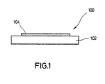
- This sensor includes a substrate 102, which is preferably made of aluminum oxide a purity of 96.5% to 99.5%, the rest of the substrate consists of other oxides on which one structured resistance layer 104 is arranged.
- the Resistance layer is a platinum-rhodium layer.
- the platinum-rhodium layer is used as the starting material a mixture of a platinum resinate paste and one Rhodium resinate paste used.
- the platinum resinate paste has 12 wt .-% platinum, the rest of the paste through an organic is formed, and the rhodium resinate paste has 7% by weight of rhodium, the rest of the Paste is formed by an organic.
- the high temperature treatment by the one described above Process eliminates structural lattice defects and an additional cleaning of the platinum-rodium layer, whereby residual organic matter still present in this layer Will get removed.
- Carrier materials to hold the structured Resistance layer may be provided, the carrier either is insulating, or is non-insulating, wherein in in this case a thin layer of insulation between the surface of the carrier and the structured resistance layer is arranged.
Landscapes
- Physics & Mathematics (AREA)
- General Physics & Mathematics (AREA)
- Engineering & Computer Science (AREA)
- Fluid Mechanics (AREA)
- Aviation & Aerospace Engineering (AREA)
- Microelectronics & Electronic Packaging (AREA)
- Manufacturing & Machinery (AREA)
- Thermistors And Varistors (AREA)
- Apparatuses And Processes For Manufacturing Resistors (AREA)
- Measuring Temperature Or Quantity Of Heat (AREA)
- Electrical Discharge Machining, Electrochemical Machining, And Combined Machining (AREA)
- Safety Valves (AREA)
- Control Of Combustion (AREA)
Description
- Bereitstellen einer Mischung aus einer Platinresinatpaste und einer Rodiumresinatpaste;
- Drucken der Mischresinatpaste mittels eines Siebdruckverfahrens auf ein Aluminiumoxid-Substrat;
- Trocknen der aufgedruckten Paste;
- Einbrennen der Paste bei einer derartigen Tmperatur über eine solche Zeitdauer, daß ein in der Schicht enthaltenes Organikum ausgebrannt wird;
- Wiederholen der letztgenannten drei Prozeßschritte auf dem gleichen Substrat, bis eine gewünschte Gesamtschichtdicke erreicht ist;
- Tempern des Substrats mit der Gesamtschicht, um einen hohen und stabilen Temperaturkoeffizienten zu erreichen.
- Fig. 1
- eine Schnittdarstellung eines Sensors zum Erfassen einer Temperatur und/oder einer Strömung gemäß einem Ausführungsbeispiel der vorliegenden Erfindung.
- Drucken der Mischresinatpaste mittels eines Siebdruckverfahrens auf ein Aluminiumoxid-Substrat mit einer Schichtdicke von etwa 15 µm.
- Trocknen der aufgedruckten Paste bei 80°C über eine Zeitdauer von 10 Minuten.
- Einbrennen der Paste in einem Durchlauf-Einbrennofen bei einer Temperatur von ungefähr 800°C, wodurch die Schichtdicke der Platin-Rodiumschicht nach dem ersten Brennen auf etwa 0,12 µm zurückgegangen ist, d. h. sehr viel Organikum wurde ausgebrannt.
- Wiederholen der ersten drei Prozeßschritte auf dem gleichen Substrat, bis eine Gesamtschichtdicke von 1,3 µm erreicht wird. Dies erfordert etwa 10 Aufdrucke der Paste und die daran anschließenden Prozeßschritte.
- Tempern des Substrats mit der Gesamtschichtdicke von 1,3 µm bei einer hohen Temperatur, bevorzugterweise 1400°C, über eine Zeitdauer von drei Stunden zusätzlich der Aufheiz- und Langsam-Abkühlzeit, um den hohen und stabilen Temperaturkoeffizienten von beispielsweise 3500 ppcm/°C zu erreichen.
Claims (5)
- Verfahren zum Herstellen eines Sensor (100) zum Erfassen einer Temperatur und/oder einer Strömung mit einem Träger (102) und einer strukturierten Widerstandsschicht (104), die auf dem Träger (102) angeordnet ist,
gekennzeichnet durch folgende Verfahrensschritte:Bereitstellen einer Mischung aus einer Platinresinatpaste und einer Rhodiumresinatpaste;Drucken der Mischresinatpaste mittels eines Siebdruckverfahrens auf ein Aluminiumoxid-Substrat;Trocknen der aufgedruckten Paste;Einbrennen der Paste bei einer derartigen Temperatur über eine solche Zeitdauer, daß ein in der Schicht enthaltener Resinatanteil ausgebrannt wird;Wiederholen der letztgenannten drei Prozeßschritte auf dem gleichen Substrat, bis eine gewünschte Gesamtschichtdicke erreicht ist;Tempern des Substrats mit der Gesamtschicht, um einen hohen und stabilen Temperaturkoeffizienten zu erreichen. - Verfahren zum Herstellen eines Sensor (100) nach Anspruch 1, dadurch gekennzeichnet,
daß bei dem Schritt des Bereitstellens der Mischung der Platinresinatpaste und der Rhodiumresinatpaste die Platinresinatpaste 12 Gew.-% Platin aufweist, wobei der Rest der Paste durch ein Resinat gebildet ist, und die Rodiumresinatpaste 7 Gew.-% Rhodium aufweist, wobei auch hier der Rest der Paste durch ein Resinat gebildet ist. - Verfahren zum Herstellen eines Sensor (100) nach Anspruch 1 oder 2, dadurch gekennzeichnet,
daß das Einbrennen der Paste bei einer Temperatur von ungefähr 800°C erfolgt. - Verfahren nach Anspruch 1, dadurch gekennzeichnet,
daß der Träger (102) aus 96,5% bis 99,5% Aluminiumoxid besteht und der Rest des Trägers aus anderen Oxiden besteht. - Verfahren nach Anspruch 1, dadurch gekennzeichnet,
daß das Verhältnis des Platinresinats zu dem Rhodiumresinat 99 Gew.-% zu 1 Gew.-% ist.
Applications Claiming Priority (3)
| Application Number | Priority Date | Filing Date | Title |
|---|---|---|---|
| DE9411235U | 1994-07-12 | ||
| DE9411235U DE9411235U1 (de) | 1994-07-12 | 1994-07-12 | Sensor zum Erfassen einer Temperatur und/oder einer Strömung |
| PCT/EP1995/002689 WO1996001983A1 (de) | 1994-07-12 | 1995-07-11 | Sensor zum erfassen einer temperatur und/oder einer strömung und verfahren zu dessen herstellung |
Publications (2)
| Publication Number | Publication Date |
|---|---|
| EP0770204A1 EP0770204A1 (de) | 1997-05-02 |
| EP0770204B1 true EP0770204B1 (de) | 1998-03-25 |
Family
ID=6911014
Family Applications (1)
| Application Number | Title | Priority Date | Filing Date |
|---|---|---|---|
| EP95926852A Expired - Lifetime EP0770204B1 (de) | 1994-07-12 | 1995-07-11 | Verfahren zum Herstellen eines Sensors zum Erfassen einer Temperatur und/oder einer Strömung |
Country Status (8)
| Country | Link |
|---|---|
| US (1) | US5853793A (de) |
| EP (1) | EP0770204B1 (de) |
| JP (1) | JP2883738B2 (de) |
| KR (1) | KR100206085B1 (de) |
| AT (1) | ATE164449T1 (de) |
| DE (2) | DE9411235U1 (de) |
| DK (1) | DK0770204T3 (de) |
| WO (1) | WO1996001983A1 (de) |
Families Citing this family (3)
| Publication number | Priority date | Publication date | Assignee | Title |
|---|---|---|---|---|
| AT405591B (de) | 1997-10-03 | 1999-09-27 | Schaffler & Co | Heizelement und verfahren zu dessen herstellung |
| DE19750123C2 (de) * | 1997-11-13 | 2000-09-07 | Heraeus Electro Nite Int | Verfahren zur Herstellung einer Sensoranordnung für die Temperaturmessung |
| CN103576956B (zh) | 2012-07-31 | 2016-08-24 | 宸鸿科技(厦门)有限公司 | 温感式触控面板及其制造方法与侦测方法 |
Family Cites Families (11)
| Publication number | Priority date | Publication date | Assignee | Title |
|---|---|---|---|---|
| US4146957A (en) * | 1977-01-17 | 1979-04-03 | Engelhard Minerals & Chemicals Corporation | Thick film resistance thermometer |
| JPS6245161Y2 (de) * | 1979-01-18 | 1987-12-02 | ||
| JPS57212347A (en) * | 1981-06-25 | 1982-12-27 | Nissan Motor Co Ltd | Air-fuel ratio control system |
| EP0140340B1 (de) * | 1983-10-28 | 1989-07-19 | NGK Spark Plug Co. Ltd. | Gasfühler mit keramischem Substrat und Verfahren zu dessen Herstellung |
| JPS6130760A (ja) * | 1984-07-24 | 1986-02-13 | Toyota Central Res & Dev Lab Inc | 酸素センサ−及びその製造方法 |
| JPH0737955B2 (ja) * | 1986-07-08 | 1995-04-26 | 富士電機株式会社 | センサ素子の電極端子部の形成方法 |
| US4808274A (en) * | 1986-09-10 | 1989-02-28 | Engelhard Corporation | Metallized substrates and process for producing |
| GB2204874B (en) * | 1987-05-19 | 1991-01-02 | Rolls Royce Plc | Temperature indicating paint and method of preparing a specimen with the same |
| JP2669699B2 (ja) * | 1989-11-28 | 1997-10-29 | 日本碍子株式会社 | 空燃比センサ |
| JPH04279003A (ja) * | 1991-03-07 | 1992-10-05 | Fuji Xerox Co Ltd | 抵抗体膜形成用ペースト |
| US5250394A (en) * | 1992-01-21 | 1993-10-05 | Industrial Technology Research Institute | Metallization method for microwave circuit |
-
1994
- 1994-07-12 DE DE9411235U patent/DE9411235U1/de not_active Expired - Lifetime
-
1995
- 1995-07-11 EP EP95926852A patent/EP0770204B1/de not_active Expired - Lifetime
- 1995-07-11 AT AT95926852T patent/ATE164449T1/de not_active IP Right Cessation
- 1995-07-11 DK DK95926852.5T patent/DK0770204T3/da active
- 1995-07-11 WO PCT/EP1995/002689 patent/WO1996001983A1/de not_active Ceased
- 1995-07-11 US US08/765,749 patent/US5853793A/en not_active Expired - Lifetime
- 1995-07-11 JP JP8504125A patent/JP2883738B2/ja not_active Expired - Fee Related
- 1995-07-11 KR KR1019970700067A patent/KR100206085B1/ko not_active Expired - Fee Related
- 1995-07-11 DE DE59501725T patent/DE59501725D1/de not_active Expired - Lifetime
Also Published As
| Publication number | Publication date |
|---|---|
| WO1996001983A1 (de) | 1996-01-25 |
| DK0770204T3 (da) | 1998-04-27 |
| US5853793A (en) | 1998-12-29 |
| JPH09510788A (ja) | 1997-10-28 |
| JP2883738B2 (ja) | 1999-04-19 |
| KR970705013A (ko) | 1997-09-06 |
| KR100206085B1 (ko) | 1999-07-01 |
| EP0770204A1 (de) | 1997-05-02 |
| ATE164449T1 (de) | 1998-04-15 |
| DE9411235U1 (de) | 1994-09-08 |
| DE59501725D1 (de) | 1998-04-30 |
Similar Documents
| Publication | Publication Date | Title |
|---|---|---|
| DE68910155T2 (de) | Mehrschichtige keramische Unterlagen und Verfahren zu ihrer Herstellung. | |
| DE2810427C3 (de) | Silbermassen für aufgedruckte Leitermuster | |
| DE1194539B (de) | Widerstandsglasurmasse | |
| DE3851548T2 (de) | Keramisches Mehrschichtsubstrat und Verfahren zu seiner Herstellung. | |
| DE3913115C2 (de) | ||
| DE3930623C2 (de) | ||
| EP0007621B1 (de) | Sauerstoffsensor | |
| EP0506676A1 (de) | Widerstandsmessfühler zur erfassung von gaszusammensetzungen und verfahren zu seiner herstellung | |
| DE69229762T2 (de) | Verfahren zur Herstellung dünner Metallfilme | |
| DE69031584T2 (de) | Schichtwiderstand und Verfahren zu seiner Herstellung | |
| EP0770204B1 (de) | Verfahren zum Herstellen eines Sensors zum Erfassen einer Temperatur und/oder einer Strömung | |
| EP0529195B1 (de) | Widerstandsmasse zur Herstellung von Dickschicht-Widerständen | |
| EP0366687B1 (de) | Herstellung von inerten, katalytisch wirksamen oder gassensitiven keramikschichten für gassensoren | |
| DE3914844C2 (de) | ||
| DE2506457C3 (de) | Verfahren zur Herstellung einer silikatischen Abdeckschicht auf einer Halbleiterscheibe öder auf einer auf ihr befindlichen Schicht | |
| DE2615473B2 (de) | Meßwiderstand für ein Widerstandsthermometer | |
| EP0432353B1 (de) | Widerstandsmasse und ihre Verwendung | |
| DE2115814C3 (de) | Widerstandspaste und Verfahren zur Herstellung eines elektrischen Dickschichtwiderstandes | |
| DE4416245C1 (de) | Verfahren zur Herstellung von PZT-Schichten aus niedrig sinterndem PZT-Pulver | |
| DE69513377T2 (de) | Widerstandspaste und dieses Material enthaltender Widerstand | |
| DE69513378T2 (de) | Widerstandspaste und dieses Material enthaltender Widerstand | |
| DE1640561B2 (de) | Widerstandsmasse | |
| DE2911346C2 (de) | Verfahren zur Herstellung eines Drahtwiderstandes | |
| DE2348779C3 (de) | Verfahren zur Herstellung geätzter Muster | |
| DE2358552B2 (de) | Verfahren zur Herstellung eines Widerstandselements |
Legal Events
| Date | Code | Title | Description |
|---|---|---|---|
| PUAI | Public reference made under article 153(3) epc to a published international application that has entered the european phase |
Free format text: ORIGINAL CODE: 0009012 |
|
| 17P | Request for examination filed |
Effective date: 19961129 |
|
| AK | Designated contracting states |
Kind code of ref document: A1 Designated state(s): AT BE CH DE DK ES FR GB IE IT LI NL SE |
|
| GRAG | Despatch of communication of intention to grant |
Free format text: ORIGINAL CODE: EPIDOS AGRA |
|
| GRAG | Despatch of communication of intention to grant |
Free format text: ORIGINAL CODE: EPIDOS AGRA |
|
| GRAG | Despatch of communication of intention to grant |
Free format text: ORIGINAL CODE: EPIDOS AGRA |
|
| GRAH | Despatch of communication of intention to grant a patent |
Free format text: ORIGINAL CODE: EPIDOS IGRA |
|
| 17Q | First examination report despatched |
Effective date: 19970807 |
|
| GRAH | Despatch of communication of intention to grant a patent |
Free format text: ORIGINAL CODE: EPIDOS IGRA |
|
| GRAA | (expected) grant |
Free format text: ORIGINAL CODE: 0009210 |
|
| ITF | It: translation for a ep patent filed | ||
| AK | Designated contracting states |
Kind code of ref document: B1 Designated state(s): AT BE CH DE DK ES FR GB IE IT LI NL SE |
|
| PG25 | Lapsed in a contracting state [announced via postgrant information from national office to epo] |
Ref country code: ES Free format text: THE PATENT HAS BEEN ANNULLED BY A DECISION OF A NATIONAL AUTHORITY Effective date: 19980325 |
|
| REF | Corresponds to: |
Ref document number: 164449 Country of ref document: AT Date of ref document: 19980415 Kind code of ref document: T |
|
| REG | Reference to a national code |
Ref country code: CH Ref legal event code: EP |
|
| GBT | Gb: translation of ep patent filed (gb section 77(6)(a)/1977) |
Effective date: 19980326 |
|
| REG | Reference to a national code |
Ref country code: DK Ref legal event code: T3 |
|
| REF | Corresponds to: |
Ref document number: 59501725 Country of ref document: DE Date of ref document: 19980430 |
|
| ET | Fr: translation filed | ||
| REG | Reference to a national code |
Ref country code: IE Ref legal event code: FG4D Free format text: 79543 |
|
| PG25 | Lapsed in a contracting state [announced via postgrant information from national office to epo] |
Ref country code: IE Free format text: LAPSE BECAUSE OF NON-PAYMENT OF DUE FEES Effective date: 19981023 |
|
| REG | Reference to a national code |
Ref country code: IE Ref legal event code: FD4D Ref document number: 79543 Country of ref document: IE |
|
| PLBE | No opposition filed within time limit |
Free format text: ORIGINAL CODE: 0009261 |
|
| STAA | Information on the status of an ep patent application or granted ep patent |
Free format text: STATUS: NO OPPOSITION FILED WITHIN TIME LIMIT |
|
| 26N | No opposition filed | ||
| REG | Reference to a national code |
Ref country code: GB Ref legal event code: IF02 |
|
| PGFP | Annual fee paid to national office [announced via postgrant information from national office to epo] |
Ref country code: AT Payment date: 20020719 Year of fee payment: 8 |
|
| PGFP | Annual fee paid to national office [announced via postgrant information from national office to epo] |
Ref country code: DK Payment date: 20020722 Year of fee payment: 8 Ref country code: BE Payment date: 20020722 Year of fee payment: 8 |
|
| PGFP | Annual fee paid to national office [announced via postgrant information from national office to epo] |
Ref country code: SE Payment date: 20020723 Year of fee payment: 8 Ref country code: NL Payment date: 20020723 Year of fee payment: 8 |
|
| PGFP | Annual fee paid to national office [announced via postgrant information from national office to epo] |
Ref country code: CH Payment date: 20020730 Year of fee payment: 8 |
|
| PG25 | Lapsed in a contracting state [announced via postgrant information from national office to epo] |
Ref country code: AT Free format text: LAPSE BECAUSE OF NON-PAYMENT OF DUE FEES Effective date: 20030711 |
|
| PG25 | Lapsed in a contracting state [announced via postgrant information from national office to epo] |
Ref country code: SE Free format text: LAPSE BECAUSE OF NON-PAYMENT OF DUE FEES Effective date: 20030712 |
|
| PG25 | Lapsed in a contracting state [announced via postgrant information from national office to epo] |
Ref country code: LI Free format text: LAPSE BECAUSE OF NON-PAYMENT OF DUE FEES Effective date: 20030731 Ref country code: DK Free format text: LAPSE BECAUSE OF NON-PAYMENT OF DUE FEES Effective date: 20030731 Ref country code: CH Free format text: LAPSE BECAUSE OF NON-PAYMENT OF DUE FEES Effective date: 20030731 Ref country code: BE Free format text: LAPSE BECAUSE OF NON-PAYMENT OF DUE FEES Effective date: 20030731 |
|
| BERE | Be: lapsed |
Owner name: *SENSOTHERM TEMPERATURSENSORIK G.M.B.H. Effective date: 20030731 |
|
| PG25 | Lapsed in a contracting state [announced via postgrant information from national office to epo] |
Ref country code: NL Free format text: LAPSE BECAUSE OF NON-PAYMENT OF DUE FEES Effective date: 20040201 |
|
| EUG | Se: european patent has lapsed | ||
| REG | Reference to a national code |
Ref country code: CH Ref legal event code: PL |
|
| NLV4 | Nl: lapsed or anulled due to non-payment of the annual fee |
Effective date: 20040201 |
|
| REG | Reference to a national code |
Ref country code: DK Ref legal event code: EBP |
|
| PGFP | Annual fee paid to national office [announced via postgrant information from national office to epo] |
Ref country code: GB Payment date: 20050620 Year of fee payment: 11 |
|
| PGFP | Annual fee paid to national office [announced via postgrant information from national office to epo] |
Ref country code: FR Payment date: 20050713 Year of fee payment: 11 |
|
| PG25 | Lapsed in a contracting state [announced via postgrant information from national office to epo] |
Ref country code: GB Free format text: LAPSE BECAUSE OF NON-PAYMENT OF DUE FEES Effective date: 20060711 |
|
| GBPC | Gb: european patent ceased through non-payment of renewal fee |
Effective date: 20060711 |
|
| REG | Reference to a national code |
Ref country code: FR Ref legal event code: ST Effective date: 20070330 |
|
| PGFP | Annual fee paid to national office [announced via postgrant information from national office to epo] |
Ref country code: IT Payment date: 20070723 Year of fee payment: 13 |
|
| PG25 | Lapsed in a contracting state [announced via postgrant information from national office to epo] |
Ref country code: FR Free format text: LAPSE BECAUSE OF NON-PAYMENT OF DUE FEES Effective date: 20060731 |
|
| PGFP | Annual fee paid to national office [announced via postgrant information from national office to epo] |
Ref country code: DE Payment date: 20080422 Year of fee payment: 14 |
|
| PG25 | Lapsed in a contracting state [announced via postgrant information from national office to epo] |
Ref country code: IT Free format text: LAPSE BECAUSE OF NON-PAYMENT OF DUE FEES Effective date: 20080711 |
|
| PG25 | Lapsed in a contracting state [announced via postgrant information from national office to epo] |
Ref country code: DE Free format text: LAPSE BECAUSE OF THE APPLICANT RENOUNCES Effective date: 20090721 |