EP0770868B1 - Procédé de contrôle de disques - Google Patents
Procédé de contrôle de disques Download PDFInfo
- Publication number
- EP0770868B1 EP0770868B1 EP96114961A EP96114961A EP0770868B1 EP 0770868 B1 EP0770868 B1 EP 0770868B1 EP 96114961 A EP96114961 A EP 96114961A EP 96114961 A EP96114961 A EP 96114961A EP 0770868 B1 EP0770868 B1 EP 0770868B1
- Authority
- EP
- European Patent Office
- Prior art keywords
- disc
- values
- reg
- degree
- reflection
- Prior art date
- Legal status (The legal status is an assumption and is not a legal conclusion. Google has not performed a legal analysis and makes no representation as to the accuracy of the status listed.)
- Expired - Lifetime
Links
Images

Classifications
-
- H—ELECTRICITY
- H05—ELECTRIC TECHNIQUES NOT OTHERWISE PROVIDED FOR
- H05K—PRINTED CIRCUITS; CASINGS OR CONSTRUCTIONAL DETAILS OF ELECTRIC APPARATUS; MANUFACTURE OF ASSEMBLAGES OF ELECTRICAL COMPONENTS
- H05K13/00—Apparatus or processes specially adapted for manufacturing or adjusting assemblages of electric components
-
- G—PHYSICS
- G01—MEASURING; TESTING
- G01R—MEASURING ELECTRIC VARIABLES; MEASURING MAGNETIC VARIABLES
- G01R31/00—Arrangements for testing electric properties; Arrangements for locating electric faults; Arrangements for electrical testing characterised by what is being tested not provided for elsewhere
- G01R31/26—Testing of individual semiconductor devices
- G01R31/265—Contactless testing
- G01R31/2656—Contactless testing using non-ionising electromagnetic radiation, e.g. optical radiation
-
- G—PHYSICS
- G01—MEASURING; TESTING
- G01N—INVESTIGATING OR ANALYSING MATERIALS BY DETERMINING THEIR CHEMICAL OR PHYSICAL PROPERTIES
- G01N21/00—Investigating or analysing materials by the use of optical means, i.e. using sub-millimetre waves, infrared, visible or ultraviolet light
- G01N21/84—Systems specially adapted for particular applications
- G01N21/88—Investigating the presence of flaws or contamination
- G01N21/8806—Specially adapted optical and illumination features
-
- G—PHYSICS
- G01—MEASURING; TESTING
- G01N—INVESTIGATING OR ANALYSING MATERIALS BY DETERMINING THEIR CHEMICAL OR PHYSICAL PROPERTIES
- G01N21/00—Investigating or analysing materials by the use of optical means, i.e. using sub-millimetre waves, infrared, visible or ultraviolet light
- G01N21/84—Systems specially adapted for particular applications
- G01N21/88—Investigating the presence of flaws or contamination
- G01N21/95—Investigating the presence of flaws or contamination characterised by the material or shape of the object to be examined
- G01N21/9501—Semiconductor wafers
-
- G—PHYSICS
- G01—MEASURING; TESTING
- G01N—INVESTIGATING OR ANALYSING MATERIALS BY DETERMINING THEIR CHEMICAL OR PHYSICAL PROPERTIES
- G01N21/00—Investigating or analysing materials by the use of optical means, i.e. using sub-millimetre waves, infrared, visible or ultraviolet light
- G01N21/84—Systems specially adapted for particular applications
- G01N21/88—Investigating the presence of flaws or contamination
- G01N21/95—Investigating the presence of flaws or contamination characterised by the material or shape of the object to be examined
- G01N21/9506—Optical discs
-
- H—ELECTRICITY
- H10—SEMICONDUCTOR DEVICES; ELECTRIC SOLID-STATE DEVICES NOT OTHERWISE PROVIDED FOR
- H10P—GENERIC PROCESSES OR APPARATUS FOR THE MANUFACTURE OR TREATMENT OF DEVICES COVERED BY CLASS H10
- H10P74/00—Testing or measuring during manufacture or treatment of wafers, substrates or devices
- H10P74/20—Testing or measuring during manufacture or treatment of wafers, substrates or devices characterised by the properties tested or measured, e.g. structural or electrical properties
- H10P74/203—Structural properties, e.g. testing or measuring thicknesses, line widths, warpage, bond strengths or physical defects
Definitions
- the invention relates to a method for checking disks, which have a layer of lacquer, in particular one Batch of such slices.
- a batch of slices as is known, several disks that are part of a single one Are manufacturing lots.
- the discs can be different Act types of disks, e.g. B. those who the manufacture of semiconductor components serve as integrated Circuits or single semiconductors or else around Disks involved in the production of a compact disc ("CD", "CD-ROM”) serve.
- CD compact disc
- CD-ROM compact disc
- panes for perfect condition e.g. control for particle freedom, i.e. free of Contamination and deposits, control for even thick layer of paint or defects in the layer of paint
- control for even thick layer of paint or defects in the layer of paint is known to be extremely important for achieving good yields in the manufacturing process.
- US-A 5091963 discloses a method and an apparatus to check surfaces for existing ones Irregularities.
- the surface is illuminated so that Light is reflected.
- a picture of the surface becomes pixel by pixel recorded by an optical device and in analyzed by a digital processing device. Based a comparison with predetermined comparison values is assessed, whether the surface is OK or faulty.
- the object of the present invention is the process of Control as flawlessly as possible and the health To be able to reduce the burden on the staff.
- German Patent application P 44 13 831.8 describes a method by means of the disks with a layer of varnish that the manufacture serve integrated semiconductor memory and at least have a first layer with structures, automatically are controllable. Devices are also described there, with which this procedure can be carried out. These devices and also the devices according to the (also older, not pre-published) German patent application P 44 13 832.6 are also to be carried out of the present invention. The revelation of these two older patent applications is also so far Part of the disclosure of the present invention, although at easier understanding of the method according to the invention below sometimes repeated.
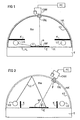
- Figure 1 shows the device, for example, on a Table T (also applies to the other two fixtures after Figures 2 and 3) or another suitable document can be arranged with a fixed stand.
- the device has a device E for receiving those to be checked Washer WF and a base plate Pl.
- the base plate However, Pl is not absolutely necessary.
- the facility E can be part of the base plate Pl. But it can also according to further configurations of the device, on the base plate Pl arranged or be embedded in this.
- the device also has a hemispherical covering device HK on, which largely with the base plate Pl closed interior Rm forms and the interior Rm an incident light Lt largely absorbing surface K1, which may be black.
- Rm is preferred, however not necessarily ring-shaped lighting device Ltl arranged that direct lighting of the WF to be checked serves.
- the ring shape enables uniform illumination of the pane WF.
- the hemispherical covering device HK points inside of the closed space Rm has a surface K1 which incident light Lt absorbed.
- Another covering device is located above the lighting device Lt1 K arranged, the incident light Lt does not let through and is absorbed if possible. she is so trained that the disc WF is directly illuminated by means of the lighting device Lt1, while the hemispherical Coverage HK largely compared to the direct Light of the lighting device Lt1 is covered. As a result these requirements are particularly in the case of ring-shaped ones Design of the lighting device Lt1 cheap, even the to design another cover device K in a ring shape.
- an image recording device CAM typically a camera, arranged so that their lens Obj into the interior Rm looks, in particular, at the point at which it is in operation the disc to be checked is located WF.
- the image capture device CAM can be arranged so that your lens Obj protrudes into the interior Rm, as shown in Figure 1, or so that the edge of your objective Obj approximately flush with the hemispherical cover HK. It is intended to be reflected by the lacquer layer L. Light Lt as an image of the to be checked Pick up the WF disc point by point.
- the image recording device CAM has an evaluation device PC connected to the control of the image recording device CAM serves as well as for reception, for temporary storage, for processing and output from the image recording device CAM transmitted data ("images").
- This Data can be transmitted analog or digital, if the image recording device CAM already for digital transmission is equipped (e.g. if it has an A / D converter).
- the evaluation device PC is typically one Computer device such as a personal computer or a data processing system. But it is also conceivable that they is formed exclusively from hardware, which is still to be described Process controls.
- the hemispherical surface K1 absorbing the light Lt HK cover is black.
- the light Lt. Emitted by the lighting device Lt1 is white.
- the further covering device K has a black surface.
- the surface of the base plate P1 is on the hemispherical Cover device HK side facing black.
- Comparison disc In the control, values of reflectance become one correspondingly reflected light from another pane (Comparison disc) used as comparison values.
- the comparison disc is regarding their production status and their Type identical to the WF disc to be checked.
- the paint and any underlying structures of the comparison disc have previously been found to be in order.
- WF panes usually have an orientation feature (at Semiconductor wafers are either due to the current Manufacturing process step already existing structures St the disk WF and / or mostly a so-called flat Ft (i.e., an area that rounds itself off Semiconductor wafer WF is flattened).
- flat Ft i.e., an area that rounds itself off Semiconductor wafer WF is flattened.
- the procedure below assumes that the wafers to be checked have such a flat Ft (see Figure 5) or another orientation feature such as Structures St (see Figure 4). The procedure works however, even if the one to be checked Disc WF has no orientation feature because the disc WF in this case, when viewed from above, is uniform, i.e. H., the image of the disk WF in the image recording device CAM is the same at every pixel, provided that the disc WF in Is okay.
- the method according to the invention also opens up the possibility that one employee can have several Devices which carry out the method according to the invention operated (e.g. placing and removing the panes, if not automated; Start of the process so far not automated) and / or controlled so that productivity can be increased again (higher productivity is known to mean lower manufacturing costs, what is nowadays is extremely important for window manufacturers).
- the pane WF to be checked is activated by means of an illumination device Ltl illuminated directly, so that the paint layer L reflects the incident light Lt.
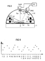
- the image capture device CAM (or CAM1 in Figure 3) captures the image the disc WF point by point, the brightness of each pixel Pixel of the image recording device CAM the value of the Represents reflectance R of the reflected light Lt, that corresponds to the pixel corresponding to the pixel Point of the surface of the lacquer L (and thus at one point the disc WF) due to the nature of the disc WF results.
- At least a majority of the reflectance values determined in this way R is from the image recording device CAM to the the connected evaluation device PC and cached.
- the values of the reflectance determined and buffered in this way R are each with one of the specified comparison values, which come from a comparison disc and which are also stored in the evaluation device PC, compared.
- the results of these comparisons are at least subject to a given assessment criterion, based on whose it is determined whether the controlled disc WF is classified as "OK" or as faulty.
- a first assessment criterion is the degree of agreement (or mismatch) that the respective determined and temporarily stored values of the reflectance R with a respectively assigned comparison value. Though in practice, the respective values and comparative values never exactly match, but is as large as possible To strive for agreement. In this respect, a (if possible smaller) tolerance value.
- a second assessment criterion is following the first assessment criterion become:
- This second assessment criterion now states that the number and / or the size of such contiguous areas Reg may not exceed a predetermined maximum. If this maximum is exceeded, the disc WF continues judged to be faulty, otherwise found to be in order.
- each disc WF is subjected to the process again under the following two changed conditions:
- the disc is illuminated indirectly (see Fig. 2 and 3) and the image recording device CAM or CAM2 is in another Angle ⁇ arranged to the surface of the disc WF, the is different from the angle ⁇ . Sense of this recheck under changed conditions is to find bugs which are in direct lighting and / or under the Recording angle ⁇ cannot be seen, but under accordingly changed conditions.
- a straight line can be defined as a fictitious measuring line Ln, which is fictitious in sections Sec is divided and if along at least one of these sections Sec the number of points, the values of which Reflectance R exceed the first assessment criterion, is greater than a given maximum value, the along the respective section Sec of this measuring line Ln is based on the total number of points whose values reflectivity R has been buffered.
- WF is used with a coherent Reg area in a border area Lim1 of this Reg area Disc areas outside this area Reg checked whether the values determined from points of this limit range Lim1 of the reflectance R is at least a factor of 10 from distinguish those values of the reflectance R which are related to Points were determined, which can be found in another Lim2 border area is located outside the Reg area. If if this is the case, the disk is rated as faulty.
- the comparison disc when determining the comparison values experience a certain orientation has (e.g. alignment at the flat Ft of a semiconductor wafer), it is favorable to also check the WF disc to be checked accordingly align because then the values of reflectance R without special coordinate conversion (regarding orientation the disc WF) can be compared directly with each other can.
Landscapes
- Physics & Mathematics (AREA)
- General Physics & Mathematics (AREA)
- Health & Medical Sciences (AREA)
- Immunology (AREA)
- Pathology (AREA)
- Life Sciences & Earth Sciences (AREA)
- Chemical & Material Sciences (AREA)
- Analytical Chemistry (AREA)
- Biochemistry (AREA)
- General Health & Medical Sciences (AREA)
- Engineering & Computer Science (AREA)
- Electromagnetism (AREA)
- Toxicology (AREA)
- Manufacturing & Machinery (AREA)
- Microelectronics & Electronic Packaging (AREA)
- Investigating Materials By The Use Of Optical Means Adapted For Particular Applications (AREA)
- Testing Or Measuring Of Semiconductors Or The Like (AREA)
- Manufacturing Optical Record Carriers (AREA)
- Optical Recording Or Reproduction (AREA)
- Analysing Materials By The Use Of Radiation (AREA)
- Automatic Analysis And Handling Materials Therefor (AREA)
- Photometry And Measurement Of Optical Pulse Characteristics (AREA)
- Exposure And Positioning Against Photoresist Photosensitive Materials (AREA)
Claims (8)
- Procédé pour contrôler des disques (WF) comportant une couche de vernis (L), qui est automatiquement mis en oeuvre avec les étapes suivantes :1) le disque (WF) est directement éclairé, de sorte que la couche de vernis (L) réfléchit la lumière (Lt),2) à l'aide d'un dispositif d'enregistrement d'image (CAM), qui saisit point par point (pixels) les images à enregistrer, et qui est disposé selon un angle prédéfini (α) au-dessus du disque (WF), et aussi à l'aide d'un dispositif d'évaluation (PC) qui y est connecté, on détermine point par point (pixels) et on mémorise d'une manière intermédiaire, pour un grand nombre de points de la surface du disque (WF), la valeur du facteur de réflexion (R) de la lumière réfléchie (It),3) les valeurs du facteur de réflexion (R) déterminées et mémorisées d'une manière intermédiaire sont comparées aux valeurs comparatives prédéfinies,4) à l'aide du résultat de la comparaison entre les valeurs déterminées et mémorisées d'une manière intermédiaire du facteur de réflexion (R) et les valeurs comparatives, on détermine, en utilisant un critère d'évaluation prédéfini, si le disque (WF) est conforme ou défectueux,
caractérisé par les étapes suivantes :5) en tant que premier critère d'évaluation, on utilise une valeur minimale prédéfinie de la concordance entre une valeur déterminée et mémorisée d'une manière intermédiaire du facteur de réflexion (R), et la valeur comparative qui lui est affectée,6) dans le cadre d'un deuxième critère d'évaluation, on procède comme suit :dans le cas dans lequel le premier critère d'évaluation dit que le disque (WF) est défectueux, on détermine la position des points du disque (WF) dont les points images (pixels) dépassent ce critère d'évaluation,à partir de la position de ces points, on détermine ceux qui, sur le disque (WF), forment des régions continues (Reg), etdans le cas dans lequel le nombre et/ou la taille des régions continues (Reg) sont inférieurs à une valeur maximale prédéfinie, le disque (WF) est considéré comme conforme,7) si le disque (WF) s'est révélé défectueux, il va, dans le cas dans lequel on contrôle un grand nombre de disques (WF), être séparé des disques (WF) qui ont été considérés comme défectueux,8) après les étapes ci-dessus :le disque (WF) est soumis à un éclairage indirect,le dispositif d'enregistrement d'image (CAM) est disposé selon un autre angle (β) par rapport à la surface du disque (WF), qui est différent de l'angle (α) prédéfini, eton procède, à l'aide de cette disposition du dispositif d'enregistrement d'image (CAM), aux étapes au moins selon les caractéristiques 2) à 4). - Procédé selon la revendication 1, caractérisé en ce que seuls sont contrôlés, à l'aide d'un éclairage indirect et du dispositif d'enregistrement d'image (CAM) disposé selon l'autre angle (β), les disques WF qui, lors du contrôle par éclairage direct et faisant appel au dispositif d'enregistrement d'image (CAM) disposé selon l'angle (α) prédéfini, ont été reconnus comme étant conformes.
- Procédé selon l'une des revendications 1 à 2, caractérisé en ce que, dans le cas dans lequel les valeurs comparatives se fondent sur une certaine orientation d'un disque comparatif utilisé lors de la détermination des valeurs comparatives, le disque (WF) à contrôler est orienté selon cette orientation.
- Procédé selon l'une des revendications 1 à 2, caractérisé en ce que, dans le cas dans lequel les valeurs comparatives se fondent sur une certaine orientation d'un disque comparatif utilisé lors de la détermination des valeurs comparatives, une orientation qui en est différente du disque (WF) à contrôler est compensée par une transformation correspondante des coordonnées des points images dont il s'agit d'enregistrer la valeur du facteur de réflexion (R).
- Procédé selon l'une des revendications précédentes, caractérisé en ce que, dans le cadre d'un troisième critère d'évaluation, on procède comme suit :
un disque (WF) qui a été considéré comme conforme d'après l'un des deux deuxièmes critères d'évaluation, est globalement évalué comme étant défectueux quand le nombre total des régions continues (Reg) a une aire totale (SQ), qui englobe ces régions (Reg) sur le disque (WF), supérieure à une portion prédéfinie de l'aire totale du disque (WF). - Procédé selon l'une des revendications précédentes, caractérisé en ce que, dans le cadre d'un quatrième critère d'évaluation, on procède comme suit :
un disque (WF) qui a été considéré comme conforme d'après l'un des deux deuxièmes critères d'évaluation est globalement évalué comme étant défectueux quand, pour au moins l'une des régions continues (Reg) il est possible de tracer une droite sous forme d'une ligne de mesure fictive (Ln), et si, le long d'au moins un segment (Sec) de cette ligne de mesure (Ln), le nombre des points dont la valeur du facteur de réflexion (R) dépasse le premier critère d'évaluation est supérieur à une valeur maximale prédéfinie, qui le long du segment considéré (Sec) de cette ligne de mesure (Ln) est rapportée au nombre total des points dont la valeur du facteur de réflexion (R) a été déterminée. - Procédé selon l'une des revendications précédentes, caractérisé en ce que, dans le cadre d'un cinquième critère d'évaluation, on procède comme suit :
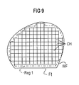
dans le cas dans lequel un disque (WF) doit, d'après les règles de l'un des deuxième, troisième ou quatrième critères d'évaluation, être évalué comme conforme, le disque (WF) est considéré comme défectueux quand, dans une région continue (Reg), les points se trouvant dans un domaine limite (Lim1) de cette région (Reg) présentent des valeurs du facteur de réflexion (R) qui se distinguent d'un facteur au moins égal à 10 des valeurs du facteur de réflexion (R) que l'on obtient pour les points qui se trouvent à l'extérieur de cette région continue et d'autres régions continues (Reg) dans un autre domaine limite (Lim2) qui entoure la région (Reg). - Procédé selon l'une des revendications précédentes, caractérisé en ce que, dans le cas dans lequel le disque (WF) comporte dans un domaine partiel (Reg1) des unités structurées (CH), l'évaluation permettant de savoir si le disque (WF) est conforme ou défectueux est, à l'extérieur de ce domaine partiel (Reg1), mise en oeuvre avec des critères plus sévères qu'à l'intérieur de ce domaine partiel (Reg1).
Applications Claiming Priority (2)
| Application Number | Priority Date | Filing Date | Title |
|---|---|---|---|
| DE19539735 | 1995-10-25 | ||
| DE19539735 | 1995-10-25 |
Publications (2)
| Publication Number | Publication Date |
|---|---|
| EP0770868A1 EP0770868A1 (fr) | 1997-05-02 |
| EP0770868B1 true EP0770868B1 (fr) | 2002-01-02 |
Family
ID=7775744
Family Applications (1)
| Application Number | Title | Priority Date | Filing Date |
|---|---|---|---|
| EP96114961A Expired - Lifetime EP0770868B1 (fr) | 1995-10-25 | 1996-09-18 | Procédé de contrôle de disques |
Country Status (7)
| Country | Link |
|---|---|
| US (1) | US5825499A (fr) |
| EP (1) | EP0770868B1 (fr) |
| JP (1) | JPH09129692A (fr) |
| KR (1) | KR970025341A (fr) |
| AT (1) | ATE211549T1 (fr) |
| DE (1) | DE59608537D1 (fr) |
| TW (1) | TW326071B (fr) |
Families Citing this family (11)
| Publication number | Priority date | Publication date | Assignee | Title |
|---|---|---|---|---|
| US6011586A (en) * | 1996-12-04 | 2000-01-04 | Cognex Corporation | Low-profile image formation apparatus |
| DE19742093A1 (de) | 1997-09-24 | 1999-03-25 | Kostal Leopold Gmbh & Co Kg | Photoelektrisches Sensorarray |
| KR100673331B1 (ko) * | 2000-02-19 | 2007-01-23 | 엘지.필립스 엘시디 주식회사 | 액정 표시장치 제조방법 및 그 제조방법에 따른액정표시장치 |
| JP3754003B2 (ja) * | 2001-06-21 | 2006-03-08 | 株式会社リコー | 欠陥検査装置及びその方法 |
| US20040196763A1 (en) * | 2001-08-10 | 2004-10-07 | Toshifumi Tanaka | Optical recording medium and manufacturing method thereof |
| JP2007269007A (ja) * | 2006-03-08 | 2007-10-18 | Ngk Insulators Ltd | スラリー塗布装置、及びスラリー塗布欠陥検査装置 |
| DE102008013387B4 (de) * | 2008-03-10 | 2020-02-13 | Byk-Gardner Gmbh | Vorrichtung zum Bestimmen optischer Oberflächeneigenschaften von Werkstücken |
| WO2014196010A1 (fr) * | 2013-06-03 | 2014-12-11 | ヤマハ発動機株式会社 | Appareil d'inspection d'apparence |
| TWI485387B (zh) * | 2013-07-31 | 2015-05-21 | Genesis Photonics Inc | 發光二極體的檢測裝置 |
| WO2017006975A1 (fr) * | 2015-07-08 | 2017-01-12 | コニカミノルタ株式会社 | Dispositif de lecture d'image et dispositif d'impression à jet d'encre |
| CN110854035A (zh) * | 2019-11-27 | 2020-02-28 | 上海华力微电子有限公司 | 晶圆边缘缺陷的检测方法及装置 |
Family Cites Families (15)
| Publication number | Priority date | Publication date | Assignee | Title |
|---|---|---|---|---|
| US3909602A (en) * | 1973-09-27 | 1975-09-30 | California Inst Of Techn | Automatic visual inspection system for microelectronics |
| JPS59157505A (ja) * | 1983-02-28 | 1984-09-06 | Hitachi Ltd | パタ−ン検査装置 |
| US4633504A (en) * | 1984-06-28 | 1986-12-30 | Kla Instruments Corporation | Automatic photomask inspection system having image enhancement means |
| JPH0671038B2 (ja) * | 1987-03-31 | 1994-09-07 | 株式会社東芝 | 結晶欠陥認識処理方法 |
| US5091963A (en) * | 1988-05-02 | 1992-02-25 | The Standard Oil Company | Method and apparatus for inspecting surfaces for contrast variations |
| JPH0786470B2 (ja) * | 1988-06-13 | 1995-09-20 | 富士写真フイルム株式会社 | ディスク表面検査方法及び装置 |
| US4975972A (en) * | 1988-10-18 | 1990-12-04 | At&T Bell Laboratories | Method and apparatus for surface inspection |
| DE4123916C2 (de) * | 1990-07-19 | 1998-04-09 | Reinhard Malz | Verfahren und Vorrichtung zum beleuchtungsdynamischen Erkennen und Klassifizieren von Oberflächenmerkmalen und -defekten eines Objektes |
| DE4032327A1 (de) * | 1990-10-11 | 1992-04-16 | Abos Automation Bildverarbeitu | Verfahren und vorrichtung zur automatisierten ueberwachung der herstellung von halbleiterbauteilen |
| JPH05129403A (ja) * | 1991-11-07 | 1993-05-25 | Toshiba Corp | ウエーハ結晶欠陥検出装置 |
| DE4324800C2 (de) * | 1993-07-23 | 1997-05-22 | Olaf Dr Ing Schnabel | Vorrichtung zur Bestimmung von Fehlern von Oberflächen hoher Güte |
| US5506793A (en) * | 1994-01-14 | 1996-04-09 | Gerber Systems Corporation | Method and apparatus for distortion compensation in an automatic optical inspection system |
| DE4410603C1 (de) * | 1994-03-26 | 1995-06-14 | Jenoptik Technologie Gmbh | Verfahren zur Erkennung von Fehlern bei der Inspektion von strukturierten Oberflächen |
| DE4413832C2 (de) * | 1994-04-20 | 2000-05-31 | Siemens Ag | Vorrichtungen zur Kontrolle von Halbleiterscheiben |
| DE4413831C2 (de) * | 1994-04-20 | 2000-05-31 | Siemens Ag | Verfahren zur Kontrolle von Halbleiterscheiben |
-
1996
- 1996-09-18 EP EP96114961A patent/EP0770868B1/fr not_active Expired - Lifetime
- 1996-09-18 AT AT96114961T patent/ATE211549T1/de not_active IP Right Cessation
- 1996-09-18 DE DE59608537T patent/DE59608537D1/de not_active Expired - Fee Related
- 1996-09-30 TW TW085111891A patent/TW326071B/zh active
- 1996-10-21 JP JP8297722A patent/JPH09129692A/ja active Pending
- 1996-10-25 KR KR1019960048186A patent/KR970025341A/ko not_active Ceased
- 1996-10-25 US US08/740,253 patent/US5825499A/en not_active Expired - Fee Related
Also Published As
| Publication number | Publication date |
|---|---|
| EP0770868A1 (fr) | 1997-05-02 |
| ATE211549T1 (de) | 2002-01-15 |
| US5825499A (en) | 1998-10-20 |
| KR970025341A (ko) | 1997-05-30 |
| JPH09129692A (ja) | 1997-05-16 |
| DE59608537D1 (de) | 2002-02-07 |
| TW326071B (en) | 1998-02-01 |
Similar Documents
| Publication | Publication Date | Title |
|---|---|---|
| EP0678910B1 (fr) | Système d'inspection de plaquettes semi-conductrices | |
| DE4413831C2 (de) | Verfahren zur Kontrolle von Halbleiterscheiben | |
| DE102004029012B4 (de) | Verfahren zur Inspektion eines Wafers | |
| EP0770868B1 (fr) | Procédé de contrôle de disques | |
| DE102021115002A1 (de) | Werkstückinspektions- und fehlererkennungssystem einschliesslich überwachung der werkstückbilder | |
| EP1027235A1 (fr) | Dispositif et procede pour la detection d'objets se trouvant sur un pare-brise | |
| DE102022123355A1 (de) | Werkstückinspektion und fehlererkennungssystem unter verwendung von farbkanälen | |
| EP1669741A1 (fr) | procédé et système pour l'inspection de Plaquettes | |
| DE4222804A1 (de) | Einrichtung und verfahren zur automatischen visuellen pruefung elektrischer und elektronischer baueinheiten | |
| DE3119688A1 (de) | Vorrichtung zur ueberpruefung eines objektes auf unregelmaessigkeiten | |
| EP2581731B1 (fr) | Dispositif et procédé de détection d'anomalies sur des instruments | |
| DE2508992A1 (de) | Verfahren zur ueberpruefung des einwandfreien zustands von bauteilen | |
| DE2753593A1 (de) | Vorrichtung zur automatischen aussenpruefung von objekten | |
| EP1158460A2 (fr) | Système et procédé de traitement d'images | |
| WO1989008836A1 (fr) | Procede et dispositif de detection de defauts dans des pieces embouties a la piece ou dans d'autres pieces a usiner | |
| EP3482348A1 (fr) | Procédé et dispositif pour catégoriser une surface de rupture d'un élément | |
| DE102007010516A1 (de) | Verfahren zur Identifizierung der Herkunft eines polykristallinen Produkts sowie Vorrichtung mit einer Bilderfassungseinheit zur Erstellung von Produktbildern eines polykristallinen Produkts | |
| EP1712898A1 (fr) | Procédé d'inspection d'une plaquette | |
| DE10331593A1 (de) | Verfahren zur Defektsegmentierung in Strukturen auf Halbleitersubstraten | |
| EP1738580A1 (fr) | Dispositif pour surveiller une zone, notamment pour securiser une zone dangereuse d'une installation automatique | |
| DE19542630C2 (de) | Vorrichtung und Verfahren zum Prüfen von Gefäßwänden | |
| DE102009009356A1 (de) | Vorrichtung und Verfahren zum Detektieren von Fehlern bei der Waferherstellung | |
| DE102009009355B4 (de) | Vorrichtung und Verfahren zum Detektieren von Fehlern bei der Waferherstellung | |
| DE10352936A1 (de) | Verfahren und Vorrichtung zur optischen Qualitätsprüfung von Objekten mit vorzugsweise kreisförmig umlaufendem Rand | |
| DE202004020330U1 (de) | Vorrichtung zur Überprüfung von Randbereichen flächiger Elemente |
Legal Events
| Date | Code | Title | Description |
|---|---|---|---|
| PUAI | Public reference made under article 153(3) epc to a published international application that has entered the european phase |
Free format text: ORIGINAL CODE: 0009012 |
|
| AK | Designated contracting states |
Kind code of ref document: A1 Designated state(s): AT DE FR GB IE IT NL |
|
| 17P | Request for examination filed |
Effective date: 19971023 |
|
| 17Q | First examination report despatched |
Effective date: 19990616 |
|
| GRAG | Despatch of communication of intention to grant |
Free format text: ORIGINAL CODE: EPIDOS AGRA |
|
| GRAG | Despatch of communication of intention to grant |
Free format text: ORIGINAL CODE: EPIDOS AGRA |
|
| GRAH | Despatch of communication of intention to grant a patent |
Free format text: ORIGINAL CODE: EPIDOS IGRA |
|
| RAP1 | Party data changed (applicant data changed or rights of an application transferred) |
Owner name: INFINEON TECHNOLOGIES AG |
|
| GRAH | Despatch of communication of intention to grant a patent |
Free format text: ORIGINAL CODE: EPIDOS IGRA |
|
| GRAA | (expected) grant |
Free format text: ORIGINAL CODE: 0009210 |
|
| REG | Reference to a national code |
Ref country code: GB Ref legal event code: IF02 |
|
| AK | Designated contracting states |
Kind code of ref document: B1 Designated state(s): AT DE FR GB IE IT NL |
|
| PG25 | Lapsed in a contracting state [announced via postgrant information from national office to epo] |
Ref country code: NL Free format text: LAPSE BECAUSE OF FAILURE TO SUBMIT A TRANSLATION OF THE DESCRIPTION OR TO PAY THE FEE WITHIN THE PRESCRIBED TIME-LIMIT Effective date: 20020102 Ref country code: IT Free format text: LAPSE BECAUSE OF FAILURE TO SUBMIT A TRANSLATION OF THE DESCRIPTION OR TO PAY THE FEE WITHIN THE PRE;WARNING: LAPSES OF ITALIAN PATENTS WITH EFFECTIVE DATE BEFORE 2007 MAY HAVE OCCURRED AT ANY TIME BEFORE 2007. THE CORRECT EFFECTIVE DATE MAY BE DIFFERENT FROM THE ONE RECORDED.SCRIBED TIME-LIMIT Effective date: 20020102 Ref country code: IE Free format text: LAPSE BECAUSE OF FAILURE TO SUBMIT A TRANSLATION OF THE DESCRIPTION OR TO PAY THE FEE WITHIN THE PRESCRIBED TIME-LIMIT Effective date: 20020102 Ref country code: GB Free format text: LAPSE BECAUSE OF FAILURE TO SUBMIT A TRANSLATION OF THE DESCRIPTION OR TO PAY THE FEE WITHIN THE PRESCRIBED TIME-LIMIT Effective date: 20020102 Ref country code: FR Free format text: LAPSE BECAUSE OF FAILURE TO SUBMIT A TRANSLATION OF THE DESCRIPTION OR TO PAY THE FEE WITHIN THE PRESCRIBED TIME-LIMIT Effective date: 20020102 |
|
| REF | Corresponds to: |
Ref document number: 211549 Country of ref document: AT Date of ref document: 20020115 Kind code of ref document: T |
|
| REG | Reference to a national code |
Ref country code: IE Ref legal event code: FG4D Free format text: GERMAN |
|
| REF | Corresponds to: |
Ref document number: 59608537 Country of ref document: DE Date of ref document: 20020207 |
|
| NLV1 | Nl: lapsed or annulled due to failure to fulfill the requirements of art. 29p and 29m of the patents act | ||
| REG | Reference to a national code |
Ref country code: IE Ref legal event code: FD4D |
|
| PG25 | Lapsed in a contracting state [announced via postgrant information from national office to epo] |
Ref country code: AT Free format text: LAPSE BECAUSE OF NON-PAYMENT OF DUE FEES Effective date: 20020918 |
|
| EN | Fr: translation not filed | ||
| PLBE | No opposition filed within time limit |
Free format text: ORIGINAL CODE: 0009261 |
|
| STAA | Information on the status of an ep patent application or granted ep patent |
Free format text: STATUS: NO OPPOSITION FILED WITHIN TIME LIMIT |
|
| 26N | No opposition filed | ||
| PG25 | Lapsed in a contracting state [announced via postgrant information from national office to epo] |
Ref country code: DE Free format text: LAPSE BECAUSE OF NON-PAYMENT OF DUE FEES Effective date: 20030401 |
|
| NLV1 | Nl: lapsed or annulled due to failure to fulfill the requirements of art. 29p and 29m of the patents act | ||
| REG | Reference to a national code |
Ref country code: HK Ref legal event code: WD Ref document number: 1004990 Country of ref document: HK |