EP0772190A2 - Verfahren und Schaltung zur Erzeugung von synchronen Steuersignalen in Videorekordern - Google Patents
Verfahren und Schaltung zur Erzeugung von synchronen Steuersignalen in Videorekordern Download PDFInfo
- Publication number
- EP0772190A2 EP0772190A2 EP96117134A EP96117134A EP0772190A2 EP 0772190 A2 EP0772190 A2 EP 0772190A2 EP 96117134 A EP96117134 A EP 96117134A EP 96117134 A EP96117134 A EP 96117134A EP 0772190 A2 EP0772190 A2 EP 0772190A2
- Authority
- EP
- European Patent Office
- Prior art keywords
- output
- time stamp
- pld
- time
- data word
- Prior art date
- Legal status (The legal status is an assumption and is not a legal conclusion. Google has not performed a legal analysis and makes no representation as to the accuracy of the status listed.)
- Granted
Links
- 238000000034 method Methods 0.000 title claims abstract description 21
- 230000001360 synchronised effect Effects 0.000 title claims description 10
- 230000015654 memory Effects 0.000 claims abstract description 12
- 238000004364 calculation method Methods 0.000 claims description 16
- 230000006870 function Effects 0.000 claims description 5
- 238000010586 diagram Methods 0.000 description 8
- 239000011159 matrix material Substances 0.000 description 3
- 230000000630 rising effect Effects 0.000 description 3
- 230000008569 process Effects 0.000 description 2
- 230000001960 triggered effect Effects 0.000 description 2
- 230000006978 adaptation Effects 0.000 description 1
- 230000008859 change Effects 0.000 description 1
- 239000002131 composite material Substances 0.000 description 1
- 230000008878 coupling Effects 0.000 description 1
- 238000010168 coupling process Methods 0.000 description 1
- 238000005859 coupling reaction Methods 0.000 description 1
- 230000010363 phase shift Effects 0.000 description 1
- 230000003936 working memory Effects 0.000 description 1
Images

Classifications
-
- G—PHYSICS
- G11—INFORMATION STORAGE
- G11B—INFORMATION STORAGE BASED ON RELATIVE MOVEMENT BETWEEN RECORD CARRIER AND TRANSDUCER
- G11B15/00—Driving, starting or stopping record carriers of filamentary or web form; Driving both such record carriers and heads; Guiding such record carriers or containers therefor; Control thereof; Control of operating function
- G11B15/02—Control of operating function, e.g. switching from recording to reproducing
- G11B15/12—Masking of heads; circuits for Selecting or switching of heads between operative and inoperative functions or between different operative functions or for selection between operative heads; Masking of beams, e.g. of light beams
- G11B15/125—Masking of heads; circuits for Selecting or switching of heads between operative and inoperative functions or between different operative functions or for selection between operative heads; Masking of beams, e.g. of light beams conditioned by the operating function of the apparatus
-
- G—PHYSICS
- G11—INFORMATION STORAGE
- G11B—INFORMATION STORAGE BASED ON RELATIVE MOVEMENT BETWEEN RECORD CARRIER AND TRANSDUCER
- G11B5/00—Recording by magnetisation or demagnetisation of a record carrier; Reproducing by magnetic means; Record carriers therefor
- G11B5/02—Recording, reproducing, or erasing methods; Read, write or erase circuits therefor
-
- G—PHYSICS
- G11—INFORMATION STORAGE
- G11B—INFORMATION STORAGE BASED ON RELATIVE MOVEMENT BETWEEN RECORD CARRIER AND TRANSDUCER
- G11B15/00—Driving, starting or stopping record carriers of filamentary or web form; Driving both such record carriers and heads; Guiding such record carriers or containers therefor; Control thereof; Control of operating function
- G11B15/02—Control of operating function, e.g. switching from recording to reproducing
- G11B15/026—Control of operating function, e.g. switching from recording to reproducing by using processor, e.g. microcomputer
-
- G—PHYSICS
- G11—INFORMATION STORAGE
- G11B—INFORMATION STORAGE BASED ON RELATIVE MOVEMENT BETWEEN RECORD CARRIER AND TRANSDUCER
- G11B15/00—Driving, starting or stopping record carriers of filamentary or web form; Driving both such record carriers and heads; Guiding such record carriers or containers therefor; Control thereof; Control of operating function
- G11B15/02—Control of operating function, e.g. switching from recording to reproducing
- G11B15/12—Masking of heads; circuits for Selecting or switching of heads between operative and inoperative functions or between different operative functions or for selection between operative heads; Masking of beams, e.g. of light beams
-
- G—PHYSICS
- G11—INFORMATION STORAGE
- G11B—INFORMATION STORAGE BASED ON RELATIVE MOVEMENT BETWEEN RECORD CARRIER AND TRANSDUCER
- G11B15/00—Driving, starting or stopping record carriers of filamentary or web form; Driving both such record carriers and heads; Guiding such record carriers or containers therefor; Control thereof; Control of operating function
- G11B15/02—Control of operating function, e.g. switching from recording to reproducing
- G11B15/12—Masking of heads; circuits for Selecting or switching of heads between operative and inoperative functions or between different operative functions or for selection between operative heads; Masking of beams, e.g. of light beams
- G11B15/14—Masking or switching periodically, e.g. of rotating heads
-
- G—PHYSICS
- G11—INFORMATION STORAGE
- G11B—INFORMATION STORAGE BASED ON RELATIVE MOVEMENT BETWEEN RECORD CARRIER AND TRANSDUCER
- G11B20/00—Signal processing not specific to the method of recording or reproducing; Circuits therefor
- G11B20/10—Digital recording or reproducing
-
- H—ELECTRICITY
- H04—ELECTRIC COMMUNICATION TECHNIQUE
- H04N—PICTORIAL COMMUNICATION, e.g. TELEVISION
- H04N5/00—Details of television systems
- H04N5/76—Television signal recording
- H04N5/91—Television signal processing therefor
- H04N5/92—Transformation of the television signal for recording, e.g. modulation, frequency changing; Inverse transformation for playback
- H04N5/926—Transformation of the television signal for recording, e.g. modulation, frequency changing; Inverse transformation for playback by pulse code modulation
-
- G—PHYSICS
- G11—INFORMATION STORAGE
- G11B—INFORMATION STORAGE BASED ON RELATIVE MOVEMENT BETWEEN RECORD CARRIER AND TRANSDUCER
- G11B15/00—Driving, starting or stopping record carriers of filamentary or web form; Driving both such record carriers and heads; Guiding such record carriers or containers therefor; Control thereof; Control of operating function
- G11B15/18—Driving; Starting; Stopping; Arrangements for control or regulation thereof
- G11B15/46—Controlling, regulating, or indicating speed
- G11B15/467—Controlling, regulating, or indicating speed in arrangements for recording or reproducing wherein both record carriers and heads are driven
- G11B15/473—Controlling, regulating, or indicating speed in arrangements for recording or reproducing wherein both record carriers and heads are driven by controlling the speed of the heads
Definitions
- the invention relates to a method and a device for generating synchronous digital control signals in video recorders, in particular in digital video recorders.
- the servo system of known digital video recorders has a sophisticated clock control circuit, since precisely defined control signals are necessary for the coordination or coupling between the motor control, for switching the head amplifier and for data exchange between the codec and the servo system.
- a sensor delivers a position pulse PU with each revolution of the scanner motor or the head drum, which forms the basis for the synchronization of the control signals.
- this position pulse PU of the scanner motor is used to carry out the synchronization with the incoming video images or video frames. Desired boundary conditions for the control signals are freedom from jitter, synchronicity, programmable phase shift and a low real-time load on the controller.
- Both SD and HD recorders require flexible, controllable head switching signals, for example HS1 and HS2, which define the write and read area.
- head switching signals for example HS1 and HS2, which define the write and read area.
- DVC standard digital video codec standard
- the mechanical tolerances can be compensated for by a programmable time delay between the sensor attached to the head drum for generating the PU signal and the switch-on edge of the head switching signal. This can be achieved with a manual adjustment process, as well as automatically using a microcomputer or microcontroller.
- a time delay value is determined which normalizes the mechanical conditions of the respective device and thus meets the required DVC standard.
- the record / play signal must also be switched synchronously with the start of the track or the start of the frame (start of the picture).
- various special operating modes such as assembly editing, insert editing and dubbing, data must be read and inserted at very specific points on a track of the video tape. In relation to the start of the track, therefore, a chronologically precise write window is to be created that controls the writing of data.
- the invention is therefore based on the object of providing a method and a device in which temporally precise, synchronous control signals are generated.
- time zero t 0 coincides with the beginning of a picture frame.
- a time stamp is a time at which one or more of the generally rectangular control signals change their level.
- This bit pattern of a time stamp t 1 , .. t n is stored as a k-bit wide data word, where k represents the number of signals, ie the number of control lines from a circuit point of view.
- the data field is output in columns according to the previous matrix definition.
- the invention comprises a circuit for carrying out the method with a microcontroller and a controllable output memory, the microcontroller having the function blocks capture register, timer, calculation unit and comparator.
- the capture register is used to record the position pulse PU, the timer to determine the time that has elapsed since time t 0 , the timer being triggered by the position pulse PU, and the comparator compares the setpoint value of the time stamp supplied by the calculation unit with that actually t 0 elapsed time, which is provided by the timer, so that in the case of equality, the controllable output memory, which has loaded the data word to be output from the calculation unit, outputs this.
- the controllable output memory is advantageously implemented by a latch.
- a flip-flop for generating a strobe pulse is arranged between the latch and the comparator of the circuit according to the invention, the set input of which is controlled by the comparator and the reset input of which is calculated by the calculation unit 5.
- the data word to be output of a time stamp is fed via a serial bus from the calculation unit into a serial / parallel converter, which processes the data for the latch.
- the serial / parallel converter and the latch can advantageously be formed by a programmable logic module, hereinafter referred to as PLD, the data word to be output of a time stamp being clocked into the PLD by means of the clock and data input of the PLD and by means of a strobe -Pulses is loaded into the output latch 10 of the PLD and output.
- PLD programmable logic module
- the next data word to be output can be read serially into the PLD, so that the PLD is prepared for outputting the data word.
- the data word of the time stamp t i-1 is loaded into the PLD so that the data word can be output when the time stamp t i occurs .
- the PLD in the circuit according to the invention can also be used as a programmable capstan FG divider.
- the advantages of the method and the circuit according to the invention lie in the rapid generation of the various synchronous control signals, a jitter-free output of time-critical pulses, an inexpensive hardware and software solution with regard to the pin assignment and the microcontroller processing time, and a simple adaptation to different servo systems, head configurations, and rotation speeds Head drum or the like justified.
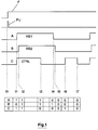
- Fig. 1 shows in the upper part of the timing diagrams of five essential signals
- the top diagram represents the image or frame signal F
- the second diagram shows the position signal PU supplied by the scanner motor, which determines the time t 0 , i.e. the time zero which is synchronous with the frame signal F.
- A, B and C denote the output signals shown in the third, fourth and fifth diagram, channel A representing the head switching signal HS1, channel B the head switching signal HS2, and channel C a control signal CTRL.
- the rising edge of the head switching signal HS1 which is synchronous with the control signal CTRL, defines a time stamp t 1 , the rising edge of the second head switching signal HS2, which is shifted by 55 ⁇ s due to the head spacing when double heads are used, a time stamp t 2 , the end of the control signal CTRL a time stamp t 3 , the end of the first head switching signal HS1 a time stamp t 4 , the falling edge of the second head switching signal HS2 a time stamp t 5 , the rising edge of the control signal CTRL another time stamp t 6 and the associated falling edge of the second control signal CTRL has a further time stamp t 7 .
- a data field assigned to the time stamps is shown, which, in accordance with the three control channels A, B, C, consists of three-bit data words which are arranged one after the other corresponding to the time stamps t 1 to t 7 in this case, so that a lookup matrix or lookup table is formed, which in this case is columnar is processed.
- the time stamp t 1 with the bit pattern 101, the time stamp t 2 with the bit pattern 111, the time stamp t 3 with the bit pattern 110, the time stamp t 4 with the Bit pattern 010, the time stamp t 5 with the bit pattern 000, the time stamp t 6 with the bit pattern 001 and the time stamp t 7 with the bit patterns 000 are connected, the control channels A, B, C being assigned the bits from left to right.
- the bit of channel A can be defined as the least significant bit (LSB) and the channel C as the most significant bit (MSB), this assignment being arbitrary and depending on the application.
- the algorithm for creating the lookup table or the data field calculates the time marks t 1 to t 7 , in general cases t 1 to t n , starting from a time zero t 0 , which is defined by the arrival of the position pulse PU, n being a natural number is the number of time stamps required in which the control pulse must be switched on one of the control lines.
- the bit pattern calculated in this way is stored in the data field and placed on the signal lines, here A, B, C, when the time stamp occurs.
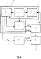
- FIG. 2 shows the circuit implementation of the method according to FIG. 1.
- the circuit essentially consists of a microcontroller 1 and a controllable output memory 2, which in the present case is implemented by an eight-fold latch 2.
- the microcontroller 1 realizes or comprises the functions of a capture register 3, a 16-bit wide timer 4, a calculation unit 5 with corresponding working memory (not shown) and a comparator 6.
- the function of the circuit is as follows: by entering the position pulse PU, which indicates the location of the head drum, the zero point of time is defined in the capture register 3 and with this input of the pulse PU, the calculation unit 5 calculates the necessary time stamps and stores them in a file field.
- the timer 4 is triggered with the input of the position pulse PU and transmits its actual value to a comparator 6.
- the comparator 6 which can be formed by a compare register of the microcontroller 1, receives the next time mark calculated by the calculation unit 5 as the target value . If the actual value and the target value in the comparator 6 are identical, a pulse is applied to the set input of a flip-flop 7, which then generates a strobe pulse and outputs it to the latch 2.
- the Latch 2 contains the data of the corresponding time stamp to be output, which were loaded from the calculation unit 5 via a serial / parallel converter 8 before the time stamp occurred. When the strobe signal arrives at the latch 2, the latter then outputs the data used as switching or control signals in parallel, so that these signals are precisely synchronized.
- connection between the calculation unit 5 and the serial / parallel converter 8 is designed as a 2-wire bus.
- the connection between the converter 8 and the latch 2 is designed in parallel, here 8-bit wide.
- PLD Programmable Logic Device
Landscapes
- Engineering & Computer Science (AREA)
- Signal Processing (AREA)
- Computer Hardware Design (AREA)
- Multimedia (AREA)
- Signal Processing For Digital Recording And Reproducing (AREA)
- Television Signal Processing For Recording (AREA)
- Management Or Editing Of Information On Record Carriers (AREA)
Abstract
Description
- Die Erfindung betrifft ein Verfahren und eine Vorrichtung zum Erzeugen von synchronen digitalen Steuersignalen in Videorekordern, insbesondere in digitalen Videorekordern.
- Das Servosystem bekannter digitaler Videorekorder weist eine ausgefeilte Taktsteuerschaltung auf, da zeitlich präzis definierte Steuersignale zur Koordinierung bzw. Verkopplung zwischen Motorsteuerung, zum Schalten der Kopfverstärker und zum Datenaustausch zwischen dem Codec- und dem Servosystem notwendig sind. Zur Definition derartiger Steuersignale liefert mit jeder Umdrehung des Scannermotors bzw. der Kopftrommel ein Sensor ein Positionspuls PU, der die Basis zur Synchronisierung der Steuersignale bildet. Unter anderem wird mit diesem Positionspuls PU des Scannermotors die Synchronisation mit den ankommenden Videobildern bzw. Videorahmen durchgeführt. Erwünschte Randbedingungen für die Steuersignale hierbei sind Jitterfreiheit, Synchronität, programmierbarer Phasenversatz und eine geringe Echtzeitbelastung des Controllers.
- Um den gewünschten Grund- und Spezialfunktionen eines Videorekorders, insbesondere eines digitalen Videorekorders gerecht zu werden, ist es zumindest nötig, folgende Schaltpulse bereitzustellen und zu erzeugen:
- ein Kopfschaltsignal HS1 zur Umschaltung von Kopf 1 und dem um 180° versetzten Kopf 2,
- ein Kopfschaltsignal HS2 zur Umschaltung von Kopf 3 und dem 180° versetzten Kopf 4,
- ein Record/Play-Umschaltsignal, und
- ein synchrones Spursignal zur alternativen Spurregelung mittels der Längsspur.
- Sowohl bei SD-, wie auch bei HD-Rekordern benötigt man flexible steuerbare Kopfschaltsignale, beispielsweise HS1 und HS2, welche den Schreib- und Lesebereich definieren. Bei 4-Kopfsystemen muß bedingt durch den geringen Abstand der Doppelköpfe von etwa 550 µm ein sehr kleiner zeitlicher Abstand der beiden Flanken der Kopfschaltsignale möglich sein, dieser Abstand beträgt bei dem genannten Kopfabstand ca. 55 µs. Um die im digitalen Videocodecstandard (DVC-Standard) definierten Spezifikationen einzuhalten, ist es außerdem erforderlich, den Schreibbeginn bezogen auf die Bandkante einzustellen. Die mechanischen Toleranzen können dabei durch eine programmierbare Zeitverzögerung zwischen dem an der Kopftrommel angebrachten Sensor zur Erzeugung des PU-Signals und der Einschaltflanke des Kopfschaltsignals ausgeglichen werden. Dies kann sowohl mit einem manuellen Justiervorgang erreicht werden, sowie auch mittels eines Mikrocomputers oder Mikrocontrollers automatisch erfolgen. Durch Auswerten von speziellen Informationen auf dem Band und deren zeitliche Zuordnung wird ein Zeitverzögerungswert ermittelt, der die mechanischen Begebenheiten des jeweiligen Gerätes normiert und somit dem geforderten DVC-Standard gerecht wird.
- Das Record/Play-Signal ist ebenfalls zeitsynchron mit dem Spurbeginn bzw. dem Rahmenbeginn (Bildbeginn) umzuschalten. Bei verschiedenen Sonderbetriebsarten, wie Assembleschnitt, Insertschnitt und Nachvertonung müssen an ganz bestimmten Stellen einer Spur des Videobandes Daten gelesen und eingefügt werden. Bezogen auf den Spuranfang ist daher ein zeitlich präzises Schreibfenster zu erzeugen, das das Einschreiben von Daten steuert.
- Der Erfindung liegt daher die Aufgabe zugrunde, ein Verfahren und eine Vorrichtung zu schaffen, worin zeitlich präzise, synchrone Steuersignale erzeugt werden.
- Diese Aufgabe wird durch die Merkmale der Ansprüche 1 und 7 gelöst. Weitere vorteilhafte Ausgestaltungen der Erfindung sind den Unteransprüchen zu entnehmen.
- Die vorliegende Erfindung betrifft ein Verfahren zur Erzeugung digitaler synchroner Steuerpulse für einen Videorekorder, insbesondere einen digitalen Videorekorder, wobei das Verfahren die folgenden Schritte aufweist:
- a) Erfassen eines Positionspulses PU des Scannermotors bzw. der Kopftrommel, der zur Definition eines Zeitnullpunktes t0 verwendet wird und die Umdrehungsperiode des Scannermotors bzw. damit der Kopftrommel bestimmt,
- b) Berechnen der Zeitmarken t1, t2, .. tn der Steuerpulse, die für die folgende Periode erforderlich sind, sowie der Bitmuster der Steuersignale zu den entsprechenden Zeitmarken,
- c) Speichern der Zeitmarken t1 - tn und der zu den entsprechenden Zeitmarken gehörenden Bitmuster,
- d) parallele Ausgabe des entsprechenden Bitmusters mit dem Eintreten einer entsprechenden Zeitmarke.
- Im allgemeinen koinzidiert der Zeitnullpunkt t0 mit dem Beginn eines Bildrahmens.
- Als eine Zeitmarke wird ein solcher Zeitpunkt bezeichnet, an dem ein oder mehrere der im allgemeinen rechteckige Steuersignale ihren Pegel ändern. Demzufolge gibt es für eine Zeitmarke jeweils ein Bitmuster, das die Pegel der einzelnen Signale enthält. Dieses Bitmuster einer Zeitmarke t1, ..tn wird als k-bit breites Datenwort abgespeichert, wobei k die Anzahl der Signale, d.h. schaltungstechnisch betrachtet die Anzahl der Steuerleitungen darstellt.
- Diese Datenwörter, deren Anzahl gleich der Anzahl n der Zeitmarken ist, werden als Datenfeld, d.h. als eine k x n Matrix, abgespeichert.
- Weiterhin wird das Datenwort der Zeitmarke ti nach dem Verstreichen der vorangegangenen Zeitmarke ti-1 in einen steuerbaren Ausgabespeicher geladen, der zur präzisen Zeitmarke ti die Ausgabe des Datenworts bewirkt, wobei

- Weiterhin umfaßt die Erfindung eine Schaltung zur Durchführung des Verfahrens mit einem Mikrocontroller und einem steuerbaren Ausgabespeicher, wobei der Mikrocontroller die Funktionsblöcke Capture-Register, Timer, Berechnungseinheit und Vergleicher aufweist. Dabei dient das Capture-Register zum Aufnehmen des Positionspulses PU, der Timer zum Bestimmen der seit dem Zeitpunkt t0 verstrichenen Zeit, wobei der Timer vom Positionspuls PU getriggert wird, und der Vergleicher vergleicht den Sollwert der von der Berechnungseinheit gelieferten Zeitmarke mit der tatsächlich seit t0 verstrichenen Zeit, die vom Timer bereitgestellt wird, so daß im Falle der Gleichheit der steuerbare Ausgabespeicher, der das auszugebende Datenwort von der Berechnungseinheit geladen hat, dieses ausgibt.
- Vorteilhafterweise wird der steuerbare Ausgabespeicher durch ein Latch realisiert. Zum Auslösen des Latchs ist zwischen dem Latch und dem Vergleicher der erfindungsgemäßen Schaltung ein Flip-Flop zur Erzeugung eines Strobe-Pulses angeordnet, dessen Set-Eingang vom Vergleicher und dessen Reset-Eingang von der Berechnungseinheit 5 angesteuert wird.
- In einer bevorzugten Ausführungsform wird das auszugebende Datenwort einer Zeitmarke über einen seriellen Bus von der Berechnungseinheit in einen Seriell/Parallel-Wandler gegeben, der die Daten für das Latch aufbereitet.
- Vorteilhafterweise kann der Seriell/Parallel-Wandler und das Latch durch einen programmierbaren Logikbaustein, im folgenden als PLD bezeichnet, gebildet werden, wobei mittel des Clock- und des Data-Eingangs des PLDs das auszugebende Datenwort einer Zeitmarke in den PLD eingetaktet und mittels eines Strobe-Pulses in das Ausgabelatch 10 des PLDs geladen und ausgegeben wird.
- Weiterhin kann nach erfolgter Ausgabe des Datenwortes einer Zeitmarke durch das Latch des PLD das nächste auszugebende Datenwort seriell in das PLD eingelesen werden, so daß das PLD zur Ausgabe des Datenworts vorbereitet ist. Mit anderen Worten, unmittelbar nachdem das Datenwort der Zeitmarke ti-1 ausgegeben wurde, wird das Datenwort der Zeitmarke ti in das PLD geladen, so daß das Datenwort beim Eintreten der Zeitmarke ti ausgegeben werden kann.
- Schließlich kann das PLD in der erfindungsgemäßen Schaltung zusätzlich als ein programmierbarer Capstan FG-Teiler verwendet werden.
- Die Vorteile des erfindungsgemäßen Verfahrens und der Schaltung liegen in einer schnellen Erzeugung der verschiedenen synchronen Steuersignale, einer jitterfreien Ausgabe von zeitkritischen Pulsen, einer preisgünstigen Hard- und Softwarelösung hinsichtlich der Pinbelegung und der Mikrocontrollerverarbeitungszeit, und einer einfachen Anpassung an verschiedene Servosysteme, Kopfkonfigurationen, Umdrehungsgeschwindigkeiten der Kopftrommel oder dergleichen begründet.
- Eine bevorzugte Ausführungsform des Verfahrens und der Schaltung wird anhand der nachfolgenden Figuren erläutert, in denen:
- Fig. 1 im oberen Teil Zeitablaufdiagramme wesentlicher Signale und im unteren Teil die Zeitmarken mit dem dazugehörigen Datenfeld zeigt,
- Fig. 2 eine erfindungsgemäße Schaltung zur Durchführung des Verfahrens zeigt, und
- Fig. 3 das Prinzipbild eines als Seriell/Parallel-Wandler und Latch verwendeten programmierbaren Logikbausteins PLD zeigt.
- Fig. 1 zeigt im oberen Teil in beispielhafter Weise die Zeitablaufdiagramme fünf wesentlicher Signale, wobei das oberste Diagramm das Bild- oder Framesignal F darstellt, das zweite Diagramm das vom Scannermotor gelieferte Positionssignal PU zeigt, das den Zeitpunkt t0, also den Zeitnullpunkt, festlegt, der synchron mit dem Framesignal F ist. Mit A, B und C werden die im dritten, vierten und fünften Diagramm dargestellten Ausgangssignale bezeichnet, wobei der Kanal A das Kopfschaltsignal HS1, der Kanal B das Kopfschaltsignal HS2, und der Kanal C ein Steuersignal CTRL darstellt. Wie aus den Diagrammen ersichtlich definiert die ansteigende Flanke des Kopfschaltsignals HS1, die synchron mit dem Steuersignal CTRL ist, eine Zeitmarke t1, die ansteigende Flanke des zweiten Kopfschaltsignals HS2, die bei der Verwendung von Doppelköpfen zeitlich um 55 µs aufgrund des Kopfabstands verschoben ist, eine Zeitmarke t2, das Ende des Steuersignals CTRL eine Zeitmarke t3, das Ende des ersten Kopfschaltsignals HS1 eine Zeitmarke t4, die fallende Flanke des zweiten Kopfschaltsignals HS2 eine Zeitmarke t5, die ansteigende Flanke des Steuersignals CTRL eine weitere Zeitmarke t6 und die dazugehörige abfallende Flanke des zweiten Steuersignales CTRL eine weitere Zeitmarke t7. Die Anzahl n = 7 ist hier nur beispielhaft zu verstehen, eine andere, insbesondere größere Anzahl ist möglich.
- Im unteren Teil der Fig. 1 ist ein den Zeitmarken zugeordnetes Datenfeld dargestellt, das entsprechend den drei Steuerkanälen A, B, C aus drei Bit breiten Datenwörtern besteht, die entsprechend den Zeitmarken t1 bis in diesem Falle t7 hintereinander angeordnet sind, so daß eine Lookup-Matrix oder eine Lookup-Tabelle gebildet wird, die in diesem Falle spaltenweise abgearbeitet wird. Aus der Zuordnung der Pulsdiagramme zu den Zeitmarken t1 bis t7 wird deutlich, daß die Zeitmarke t1 mit dem Bitmuster 101, die Zeitmarke t2 mit dem Bitmuster 111, die Zeitmarke t3 mit dem Bitmuster 110, die Zeitmarke t4 mit dem Bitmuster 010, die Zeitmarke t5 mit dem Bitmuster 000, die Zeitmarke t6 mit dem Bitmuster 001 und die Zeitmarke t7 mit den Bitmustern 000 verbunden ist, wobei den Steuerkanälen A, B, C die Bits von links nach rechts zugeordnet sind. Im vorliegenden Falle kann das Bit des Kanals A als niedrigstwertiges Bit (LSB) und der Kanal C als höchstwertiges Bit (MSB) definiert werden, wobei diese Zuordnung willkürlich ist und von der Anwendung abhängt.
- Der Algorithmus zur Erstellung der Lookup-Tabelle bzw. des Datenfeldes errechnet ausgehend von einem Zeitnullpunkt t0, der durch das Eintreffen des Positionspulses PU definiert ist, die Zeitmarken t1 bis t7, im allgemeinen Falle t1 bis tn, wobei n eine natürliche Zahl ist entsprechend der Anzahl der benötigten Zeitmarken, in denen auf einem der Steuerleitungen eine Umschaltung des Steuerpulses zu geschehen hat. Das so errechnete Bitmuster wird in dem Datenfeld gespeichert und mit dem Eintreten der Zeitmarke auf die Signalleitungen, hier A, B, C, gelegt.
- Fig. 2 zeigt die schaltungsmäßige Realisierung des Verfahrens nach der Fig. 1. Die Schaltung besteht dabei im wesentlichen aus einem Mikrocontroller 1 und einem steuerbaren Ausgabespeicher 2, der im vorliegenden Fall durch ein Achtfach-Latch 2 realisiert ist. Der Mikrocontroller 1 realisiert bzw. umfaßt die Funktionen eines Capture Registers 3, eines 16-Bit breiten Zeitgebers 4, einer Berechnungseinheit 5 mit entsprechendem Arbeitsspeicher (nicht dargestellt) und eines Vergleichers 6. Die Funktion der Schaltung ist die folgende: mit der Eingabe des Positionspulses PU, der den Ort der Kopftrommel angibt, in das Capture-Register 3 wird der Zeitnullpunkt definiert und mit diesem Eingang des Pulses PU berechnet die Berechnungseinheit 5 die notwendigen Zeitmarken und legt diese in ein Dateifeld ab. Der Zeitgeber 4 wird mit dem Eingang des Positionspulses PU getriggert und gibt seinen IST-Wert an einen Vergleicher 6. Der Vergleicher 6, der durch ein Compare-Register des Mikrocontrollers 1 gebildet werden kann, erhält als Sollwert die nächste von der Berechnungseinheit 5 berechnete Zeitmarke. Bei einer Gleichheit des Ist- und des Sollwerts im Vergleicher 6 wird ein Puls auf den Set-Eingang eines Flip-Flops 7 gegeben, welches daraufhin einen Strobepuls erzeugt und an das Latch 2 ausgibt. Das Latch 2 enthält die auszugebenden Daten der entsprechenden Zeitmarke, die vor dem Eintreten der Zeitmarke über einen Seriell/Parallel-Wandler 8 aus der Berechnungseinheit 5 geladen wurden. Mit dem Eintreffen des Strobesignals an dem Latch 2 gibt dieses dann die als Schalt- bzw. Steuersignale verwendeten Daten parallel aus, so daß eine exakte Synchronisierung dieser Signale gegeben ist.
- In der bevorzugten Ausführungsform ist die Verbindung zwischen der Berechnungseinheit 5 und dem Seriell/Parallel-Wandler 8 als 2-Draht Bus ausgelegt Die Verbindung zwischen dem Wandler 8 und dem Latch 2 ist parallel, hier 8-bit breit, ausgelegt.
- Fig. 3 zeigt die Realisierung des Latchs 2 und des Seriell/Parallel-Wandlers 8 in Form eines programmierbaren Logikbausteins (PLD = Programmable Logic Device). Mittels der beiden Leitungen "Data" und "Clock" werden das 8 Bit breite Datenwort und ein hier nicht weiter erklärter 5 Bit breiter Capstan FG-Teilerwert als zusammengesetztes 13 Bit-Datenwort vom Mikrocontroller seriell in das PLD 9 getaktet. Zwar wurden in der Fig. 1 nur das Bereitstellen von drei Steuersignalen HS1, HS2 und CTRL erläutert. Allerdings ist es selbstverständlich, daß weitere parallele Steuersignale generiert werden können, falls dies notwendig ist. Mit dem Eintreffen des Strobesignals werden die beiden Datenwortsegmente in die beiden Latches 10 und 11 des PLD 9 geladen und ausgegeben. Nach erfolgter Ausgabe der Steuersignale über das Latch 10 des PLD 9 kann bereits das nächste auszugebende Datenwort seriell in das PLD eingelesen werden.
-
- 1
- - µ-Controller
- 2
- - Ausgabespeicher (Latch)
- 3
- - Capture Register
- 4
- - 16 Bit-Timer
- 5
- - Berechnungseinheit
- 6
- - Vergleicher
- 7
- - Flip-Flop
- 8
- - Seriell/Parallel-Wandler
- 9
- - PLD
- 10
- - Latch des PLD
- 11
- - Latch des PLD
- A
- - Ausgang
- B
- - Ausgang
- C
- - Ausgang
- HS1
- - Kopfschaltsignal
- HS2
- - Kopfschaltsignal
- CTRL
- - Controlsignal
- PU
- - Positionsignal
- F
- - Framesignal
Claims (13)
- Verfahren zur Erzeugung synchroner digitaler Steuersignale für einen Videorekorder, insbesondere einen digitalen Videorekorder, gekennzeichnet durch die folgenden Schritte:a) Übernahme eines Positionspulses (PU), der zur Definition eines Zeitnullpunktes (t0) verwendet wird und eine Periode einer Kopfumdrehung definiert,b) Berechnen aller Zeitmarken (t1, t2, ..) der Steuersignale, die für die folgende Periode erforderlich sind, sowie der zu einer Zeitmarke gehörenden Bitmuster der Steuersignale,c) Speichern der Zeitmarken (t1 - tn) und der auszugebenden Bitmusters,d) Parallele Ausgabe des entsprechenden Bitmusters zur entsprechenden Zeitmarke.
- Verfahren nach Anspruch 1, dadurch gekennzeichnet, daß der Zeitnullpunkt (t0) mit dem Beginn eines Bildrahmens (F) koinzidiert.
- Verfahren nach einem der Ansprüche 1 oder 2, dadurch gekennzeichnet, daß das Bitmuster einer Zeitmarke (t1, ..tn) als k-bitbreites Datenwort abgespeichert wird.
- Verfahren nach Anspruch 3, dadurch gekennzeichnet, daß die n-Datenwörter als Datenfeld abgespeichert werden.
- Verfahren nach Anspruch 4, dadurch gekennzeichnet, daß das Datenwort der Zeitmarke (ti) nach dem Verstreichen der vorangegangenen Zeitmarke (ti-1) in einen Ausgabespeicher geladen wird, der mit dem Eintreten der Zeitmarke (ti) die Ausgabe des Datenworts bewirkt.
- Verfahren nach einem der vorangegangenen Ansprüche, dadurch gekennzeichnet, daß das Positionssignal (PU) durch einen Sensor am Scannermotor erzeugt wird.
- Schaltung zur Durchführung des Verfahrens nach einem der Ansprüche 1 bis 6, wobei die Schaltung einen Mikrocontroller (1) und einen steuerbaren Ausgabespeicher (2) derart umfaßt, daß der Mikrocontroller (1) die Funktionsblöcke Capture-Register (3) zum Aufnehmen des Positionspulses (PU), Timer (4), Berechnungseinheit (5) und Vergleicher (6) aufweist, wobei der Vergleicher (6) den Sollwert der von der Berechnungseinheit (5) gelieferten Zeitmarke mit der aktuellen Zeitmarke des Timers (4) vergleicht, so daß im Falle der Gleichheit der steuerbare Ausgabespeicher (2), der das auszugebende Datenwort von der Berechnungseinheit (5) geladen hat, dieses ausgibt.
- Schaltung nach Anspruch 7, dadurch gekennzeichnet, daß der steuerbare Ausgabespeicher (2) durch ein Latch (2) realisiert ist.
- Schaltung nach Anspruch 8, dadurch gekennzeichnet, daß zwischen dem Latch (2) und dem Vergleicher (6) ein Flip-Flop (7) zur Erzeugung eines Strobe-Pulses angeordnet ist, dessen Set-Eingang vom Vergleicher (6) und dessen Reset-Eingang von der Berechnungseinheit (5) angesteuert wird.
- Schaltung nach Anspruch 9, dadurch gekennzeichnet, daß das auszugebende Datenwort einer Zeitmarke (ti) über einen seriellen Bus von der Berechnungseinheit (5) in einen Seriell/Parallel-Wandler (8) gegeben wird, der die Daten für das Latch (2) aufbereitet.
- Schaltung nach Anspruch 10, dadurch gekennzeichnet, daß der Seriell/Parallel-Wandler (8) und das Latch (2) durch ein PLD (9) gebildet wird, wobei mittels des Clock- und des Data-Eingangs des PLDs (9) das auszugebende Datenwort einer Zeitmarke (ti) in das PLD (9) eingetaktet und mittels eines Strobe-Pulses in ein Ausgabelatch (10) des PLDs (9) geladen und ausgegeben wird.
- Schaltung nach Anspruch 11, dadurch gekennzeichnet, daß nach erfolgter Ausgabe des Datenwortes einer Zeitmarke (ti) durch das Latch (10) des PLD (9) das nächste auszugebende Datenwort seriell in das PLD (9) eingelesen werden kann.
- Schaltung nach einem der Ansprüche 11 oder 12, dadurch gekennzeichnet, daß das PLD (9) zusätzlich als ein programmierbarer Capstan FG-Teiler verwendet wird.
Applications Claiming Priority (2)
| Application Number | Priority Date | Filing Date | Title |
|---|---|---|---|
| DE19540752 | 1995-11-02 | ||
| DE19540752A DE19540752A1 (de) | 1995-11-02 | 1995-11-02 | Verfahren und Schaltung zur Erzeugung von synchronen Steuersignalen in Videorekordern |
Publications (3)
| Publication Number | Publication Date |
|---|---|
| EP0772190A2 true EP0772190A2 (de) | 1997-05-07 |
| EP0772190A3 EP0772190A3 (de) | 2001-01-10 |
| EP0772190B1 EP0772190B1 (de) | 2004-07-21 |
Family
ID=7776392
Family Applications (1)
| Application Number | Title | Priority Date | Filing Date |
|---|---|---|---|
| EP96117134A Expired - Lifetime EP0772190B1 (de) | 1995-11-02 | 1996-10-25 | Verfahren und Schaltung zur Erzeugung von synchronen Steuersignalen in Videorekordern |
Country Status (7)
| Country | Link |
|---|---|
| US (1) | US5911034A (de) |
| EP (1) | EP0772190B1 (de) |
| JP (1) | JP3809235B2 (de) |
| KR (1) | KR100416868B1 (de) |
| CN (1) | CN1121115C (de) |
| DE (2) | DE19540752A1 (de) |
| MY (1) | MY128716A (de) |
Cited By (1)
| Publication number | Priority date | Publication date | Assignee | Title |
|---|---|---|---|---|
| EP1209675A1 (de) * | 2000-11-24 | 2002-05-29 | Thomson Licensing S.A. | Kopfschaltungssteurgerät für einen Magnetbandrecorder |
Family Cites Families (13)
| Publication number | Priority date | Publication date | Assignee | Title |
|---|---|---|---|---|
| EP0138210A3 (de) * | 1983-10-14 | 1986-02-05 | Hitachi, Ltd. | Magnetisches Aufnahme- oder Wiedergabegerät der Art mit Drehkopf und Verfahren zum Erzeugen von Spurnachlaufsteuersignalen |
| JPS6113464A (ja) * | 1984-06-29 | 1986-01-21 | Hitachi Ltd | 磁気記録再生装置 |
| DE3436457A1 (de) * | 1984-10-05 | 1986-04-10 | Deutsche Thomson-Brandt Gmbh, 7730 Villingen-Schwenningen | Verfahren zur erzeugung des kopfschaltsignals und des vertikalsynchronsignals bei videorecordern |
| JPH0646479B2 (ja) * | 1987-05-18 | 1994-06-15 | 株式会社日立製作所 | モ−タ回転制御装置 |
| DE3739283A1 (de) * | 1987-11-20 | 1989-06-01 | Broadcast Television Syst | Videomagnetbandgeraet |
| US4935826A (en) * | 1988-02-08 | 1990-06-19 | Goldstar Co. Ltd. | Automatic tracking device for video cassette tape recorder |
| DE3810988C1 (de) * | 1988-03-31 | 1989-05-24 | Nokia Graetz Gmbh, 7000 Stuttgart, De | |
| US5142420A (en) * | 1989-04-28 | 1992-08-25 | Matsushita Electric Industrial Co., Ltd. | Sampling frequency reproduction system |
| US5745314A (en) * | 1989-09-27 | 1998-04-28 | Canon Kabushiki Kaisha | Clock generating circuit by using the phase difference between a burst signal and the oscillation signal |
| DE4107729A1 (de) * | 1991-03-11 | 1992-09-17 | Philips Patentverwaltung | Anordnung zur erzeugung von digitalsignalen |
| US5357382A (en) * | 1991-06-21 | 1994-10-18 | Goldstar Co., Ltd. | Apparatus and method for automatically controlling adjustment of head switching point by using vertical synchronization signal in VCR |
| US5448367A (en) * | 1992-07-02 | 1995-09-05 | Goldstar Co., Ltd. | Apparatus for automatically controlling generation of a head switching signal |
| DE4338391A1 (de) * | 1993-11-10 | 1995-05-11 | Philips Patentverwaltung | Vorrichtung zur Erzeugung von Kopfschaltsignalen für ein Magnetbandgerät |
-
1995
- 1995-11-02 DE DE19540752A patent/DE19540752A1/de not_active Withdrawn
-
1996
- 1996-10-09 US US08/648,809 patent/US5911034A/en not_active Expired - Lifetime
- 1996-10-11 CN CN96112416A patent/CN1121115C/zh not_active Expired - Fee Related
- 1996-10-25 EP EP96117134A patent/EP0772190B1/de not_active Expired - Lifetime
- 1996-10-25 DE DE59611040T patent/DE59611040D1/de not_active Expired - Lifetime
- 1996-10-31 KR KR1019960050532A patent/KR100416868B1/ko not_active Expired - Fee Related
- 1996-10-31 JP JP29044496A patent/JP3809235B2/ja not_active Expired - Fee Related
- 1996-11-02 MY MYPI96004574A patent/MY128716A/en unknown
Non-Patent Citations (1)
| Title |
|---|
| None |
Cited By (2)
| Publication number | Priority date | Publication date | Assignee | Title |
|---|---|---|---|---|
| EP1209675A1 (de) * | 2000-11-24 | 2002-05-29 | Thomson Licensing S.A. | Kopfschaltungssteurgerät für einen Magnetbandrecorder |
| WO2002043062A3 (en) * | 2000-11-24 | 2002-08-08 | Thomson Licensing Sa | Head switching control apparatus for a magnetic tape recorder |
Also Published As
| Publication number | Publication date |
|---|---|
| EP0772190B1 (de) | 2004-07-21 |
| DE59611040D1 (de) | 2004-08-26 |
| JPH09171662A (ja) | 1997-06-30 |
| US5911034A (en) | 1999-06-08 |
| EP0772190A3 (de) | 2001-01-10 |
| JP3809235B2 (ja) | 2006-08-16 |
| CN1121115C (zh) | 2003-09-10 |
| CN1152838A (zh) | 1997-06-25 |
| DE19540752A1 (de) | 1997-05-07 |
| MY128716A (en) | 2007-02-28 |
| KR970029339A (ko) | 1997-06-26 |
| KR100416868B1 (ko) | 2004-05-27 |
Similar Documents
| Publication | Publication Date | Title |
|---|---|---|
| DE3151251C2 (de) | ||
| DE2703579C2 (de) | Anordnung zur Verarbeitung von Videosignalen | |
| DE2907527C2 (de) | ||
| DE3114924C2 (de) | Schneller Zeittaktsignalgenerator | |
| DE2302587B2 (de) | Verfahren zur simultanen Multiplex-Aufzeichnung und -wiedergabe von Bild- und Mehrkanaldatensignalen sowie Einrichtung hierfür | |
| EP0224302B1 (de) | Schaltungsanordnung zum Erhöhen der Schärfe von Farbkanten | |
| DE2654050B2 (de) | Taktsignalsteuersystem eines Mikrocomputersystems | |
| AT389787B (de) | Zeitzaehltaktgenerator | |
| DE2023693A1 (de) | ||
| DE3032673C2 (de) | ||
| DE3633280C2 (de) | ||
| DE2433885C3 (de) | Vorrichtung zum Synchronisieren der Eingansschaltung eines elektronischen Testinstruments auf zu prüfende Signalfolgen | |
| DE3512059C2 (de) | ||
| DE1281494B (de) | Einrichtung zur Korrektur der Schraeglauf-Abfuehlung eines bandfoermigen Mehrspur-Aufzeichnungstraegers | |
| DE3225365C2 (de) | ||
| DE3237848C2 (de) | Korrekturvorrichtung zum Synchronisieren von durch Lage- und Schräglauffehler verursachten Daten-Zeitversätzen | |
| EP0772190B1 (de) | Verfahren und Schaltung zur Erzeugung von synchronen Steuersignalen in Videorekordern | |
| EP0215141B1 (de) | Verfahren zur Steuerung von Zeilendruckern mit einem umlaufenden Typenband und einer Druckhammerbank | |
| DE3212450A1 (de) | Synchronisiereinrichtung einer digitalsignal-demultiplexeinrichung | |
| DE3687083T2 (de) | Verfahren und vorrichtung zur erzeugung von halbtonpunkten. | |
| DE3810988C1 (de) | ||
| DE69032309T2 (de) | Verfahren und Vorrichtung zum Identifizieren der Wiedergabe-Art | |
| DE4234346C2 (de) | Horizontal-Oszillationsschaltung | |
| DE2747447C2 (de) | ||
| EP0179526A2 (de) | Abtastregelkreis |
Legal Events
| Date | Code | Title | Description |
|---|---|---|---|
| PUAI | Public reference made under article 153(3) epc to a published international application that has entered the european phase |
Free format text: ORIGINAL CODE: 0009012 |
|
| AK | Designated contracting states |
Kind code of ref document: A2 Designated state(s): DE FR GB IT |
|
| PUAL | Search report despatched |
Free format text: ORIGINAL CODE: 0009013 |
|
| AK | Designated contracting states |
Kind code of ref document: A3 Designated state(s): DE FR GB IT |
|
| RIC1 | Information provided on ipc code assigned before grant |
Free format text: 7G 11B 15/12 A, 7G 11B 15/14 B |
|
| 17P | Request for examination filed |
Effective date: 20010703 |
|
| 17Q | First examination report despatched |
Effective date: 20020926 |
|
| GRAP | Despatch of communication of intention to grant a patent |
Free format text: ORIGINAL CODE: EPIDOSNIGR1 |
|
| GRAS | Grant fee paid |
Free format text: ORIGINAL CODE: EPIDOSNIGR3 |
|
| GRAA | (expected) grant |
Free format text: ORIGINAL CODE: 0009210 |
|
| AK | Designated contracting states |
Kind code of ref document: B1 Designated state(s): DE FR GB IT |
|
| REG | Reference to a national code |
Ref country code: GB Ref legal event code: FG4D Free format text: NOT ENGLISH |
|
| REF | Corresponds to: |
Ref document number: 59611040 Country of ref document: DE Date of ref document: 20040826 Kind code of ref document: P |
|
| GBT | Gb: translation of ep patent filed (gb section 77(6)(a)/1977) |
Effective date: 20040826 |
|
| REG | Reference to a national code |
Ref country code: GB Ref legal event code: 746 Effective date: 20040903 |
|
| ET | Fr: translation filed | ||
| REG | Reference to a national code |
Ref country code: FR Ref legal event code: D6 |
|
| PLBE | No opposition filed within time limit |
Free format text: ORIGINAL CODE: 0009261 |
|
| STAA | Information on the status of an ep patent application or granted ep patent |
Free format text: STATUS: NO OPPOSITION FILED WITHIN TIME LIMIT |
|
| 26N | No opposition filed |
Effective date: 20050422 |
|
| PGFP | Annual fee paid to national office [announced via postgrant information from national office to epo] |
Ref country code: IT Payment date: 20071027 Year of fee payment: 12 |
|
| PG25 | Lapsed in a contracting state [announced via postgrant information from national office to epo] |
Ref country code: IT Free format text: LAPSE BECAUSE OF NON-PAYMENT OF DUE FEES Effective date: 20081025 |
|
| PGFP | Annual fee paid to national office [announced via postgrant information from national office to epo] |
Ref country code: DE Payment date: 20121019 Year of fee payment: 17 Ref country code: FR Payment date: 20121119 Year of fee payment: 17 |
|
| PGFP | Annual fee paid to national office [announced via postgrant information from national office to epo] |
Ref country code: GB Payment date: 20121026 Year of fee payment: 17 |
|
| GBPC | Gb: european patent ceased through non-payment of renewal fee |
Effective date: 20131025 |
|
| PG25 | Lapsed in a contracting state [announced via postgrant information from national office to epo] |
Ref country code: GB Free format text: LAPSE BECAUSE OF NON-PAYMENT OF DUE FEES Effective date: 20131025 |
|
| REG | Reference to a national code |
Ref country code: FR Ref legal event code: ST Effective date: 20140630 |
|
| REG | Reference to a national code |
Ref country code: DE Ref legal event code: R119 Ref document number: 59611040 Country of ref document: DE Effective date: 20140501 |
|
| PG25 | Lapsed in a contracting state [announced via postgrant information from national office to epo] |
Ref country code: DE Free format text: LAPSE BECAUSE OF NON-PAYMENT OF DUE FEES Effective date: 20140501 Ref country code: FR Free format text: LAPSE BECAUSE OF NON-PAYMENT OF DUE FEES Effective date: 20131031 |