EP0772199A2 - Nichtflüchtiges Register und seine Datenzugriffsverfahren - Google Patents
Nichtflüchtiges Register und seine Datenzugriffsverfahren Download PDFInfo
- Publication number
- EP0772199A2 EP0772199A2 EP96116663A EP96116663A EP0772199A2 EP 0772199 A2 EP0772199 A2 EP 0772199A2 EP 96116663 A EP96116663 A EP 96116663A EP 96116663 A EP96116663 A EP 96116663A EP 0772199 A2 EP0772199 A2 EP 0772199A2
- Authority
- EP
- European Patent Office
- Prior art keywords
- electrode
- capacitor
- coupled
- voltage
- data
- Prior art date
- Legal status (The legal status is an assumption and is not a legal conclusion. Google has not performed a legal analysis and makes no representation as to the accuracy of the status listed.)
- Withdrawn
Links
- 238000000034 method Methods 0.000 title claims abstract description 11
- 239000003990 capacitor Substances 0.000 claims abstract description 222
- 230000010287 polarization Effects 0.000 claims abstract description 65
- 230000000295 complement effect Effects 0.000 claims abstract description 29
- 238000000605 extraction Methods 0.000 claims abstract description 20
- 238000007599 discharging Methods 0.000 claims description 19
- 230000004913 activation Effects 0.000 claims description 8
- 230000014759 maintenance of location Effects 0.000 claims 12
- 230000008859 change Effects 0.000 description 8
- 230000005684 electric field Effects 0.000 description 8
- 238000010586 diagram Methods 0.000 description 7
- 230000007935 neutral effect Effects 0.000 description 6
- 230000006870 function Effects 0.000 description 3
- 230000000630 rising effect Effects 0.000 description 3
- 239000004065 semiconductor Substances 0.000 description 3
- 230000008901 benefit Effects 0.000 description 2
- 230000005669 field effect Effects 0.000 description 2
- 230000008569 process Effects 0.000 description 2
- XUIMIQQOPSSXEZ-UHFFFAOYSA-N Silicon Chemical compound [Si] XUIMIQQOPSSXEZ-UHFFFAOYSA-N 0.000 description 1
- 230000009286 beneficial effect Effects 0.000 description 1
- 238000013507 mapping Methods 0.000 description 1
- 229910044991 metal oxide Inorganic materials 0.000 description 1
- 150000004706 metal oxides Chemical class 0.000 description 1
- 229910052710 silicon Inorganic materials 0.000 description 1
- 239000010703 silicon Substances 0.000 description 1
Images

Classifications
-
- G—PHYSICS
- G11—INFORMATION STORAGE
- G11C—STATIC STORES
- G11C16/00—Erasable programmable read-only memories
- G11C16/02—Erasable programmable read-only memories electrically programmable
- G11C16/06—Auxiliary circuits, e.g. for writing into memory
-
- G—PHYSICS
- G11—INFORMATION STORAGE
- G11C—STATIC STORES
- G11C14/00—Digital stores characterised by arrangements of cells having volatile and non-volatile storage properties for back-up when the power is down
- G11C14/0054—Digital stores characterised by arrangements of cells having volatile and non-volatile storage properties for back-up when the power is down in which the volatile element is a SRAM cell
- G11C14/0072—Digital stores characterised by arrangements of cells having volatile and non-volatile storage properties for back-up when the power is down in which the volatile element is a SRAM cell and the nonvolatile element is a ferroelectric element
-
- G—PHYSICS
- G11—INFORMATION STORAGE
- G11C—STATIC STORES
- G11C11/00—Digital stores characterised by the use of particular electric or magnetic storage elements; Storage elements therefor
- G11C11/21—Digital stores characterised by the use of particular electric or magnetic storage elements; Storage elements therefor using electric elements
- G11C11/22—Digital stores characterised by the use of particular electric or magnetic storage elements; Storage elements therefor using electric elements using ferroelectric elements
Definitions
- the present invention relates, in general, to non-volatile memory elements, and more particularly, to ferroelectric non-volatile registers.
- Non-volatile configuration registers are commonly used for memory mapping and security purposes. These non-volatile registers can be implemented as stand alone registers or as part of a non-volatile memory array such as an electrical erasable programmable read only memory (EEPROM).
- EEPROM electrical erasable programmable read only memory
- An advantage of having the non-volatile registers as a portion of an EEPROM is the convenience it affords in realizing a long register. However, if the register is only a single byte in length then this technique becomes inefficient in terms of area, speed, and power. For example, access of non-volatile registers in an EEPROM requires a sense amplifier that needs to be activated. The sense amplifier consumes a large amount of power and occupies a large area on a semiconductor die. Further, the non-volatile register shares a highly capacitive bit line with a memory array. This capacitance slows down the access of the register and requires additional power for charging and discharging.
- a row of the memory array is normally used.
- a single row of the memory array typically consists of 128 or 256 bits, depending on the memory array structure. Since a register only requires a few bits, using a memory array structure to implement a register leaves a large number of bits of the memory array unused and, therefore, wastes a large portion of the memory array. This unused portion of the memory array consumes a large portion of the semiconductor die which is also wasted.
- registers are separate from the memory array structure. It would be of further advantage for the registers to be modular and capable of being cascaded to form memory blocks of different sizes. It is also desirable that accessing data in the register be simple, fast, and energy efficient.
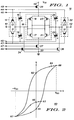
- FIG. 1 is a schematic diagram of a non-volatile register 10 in accordance with an embodiment of the present invention.
- Register 10 includes pass gates 12 and 32, ferroelectric capacitors 14, 16, 24, and 26, a voltage detector 18, and transistors 27 and 28.
- Pass gate 12 includes an n-channel metal oxide semiconductor field effect transistor (MOSFET) 11 and a p-channel MOSFET 13.
- MOSFET 11 serves as a first control electrode of pass gate 12 and is connected to a node 43 for receiving a control signal.
- a gate electrode of MOSFET 13 serves as a second control electrode of pass gate 12 and is connected to a node 44 for receiving a complementary control signal.
- a source electrode of MOSFET 11 is connected to a source electrode of MOSFET 13 to form a first data electrode of pass gate 12.
- the first data electrode of pass gate 12 is connected to a node 41 for transmitting a data signal.
- a drain electrode of MOSFET 11 is connected to a drain electrode of MOSFET 13 to form a second data electrode of pass gate 12.
- pass gate 12 is not limited to the embodiment shown in FIG. 1. Suitable structures for pass gate 12 include pass gates capable of transmitting logical signals in two directions, single transistor pass gates having a single control electrode, or the like. As those skilled in the art are aware, the control signal applied to the control electrode of a single transistor pass gate structure may be different from the control signals applied to the control electrodes of a multi-transistor pass gate structure, e.g., pass gate 12.
- a first electrode of capacitor 14 is connected to a node 45 for receiving an extraction signal.
- a second electrode of capacitor 14 is connected to the second data electrode of pass gate 12 and to a first electrode of capacitor 16.
- a second electrode of capacitor 16 is connected to a node 46 for receiving a restoration signal.
- Voltage detector 18 includes n-channel MOSFETs 17 and 21, and p-channel MOSFETs 19 and 23.
- MOSFETs 17 and 19 form a first inverter and MOSFETs 21 and 23 form a second inverter.
- a gate electrode of MOSFET 17 is connected to a gate electrode of MOSFET 19 to form an input of the first inverter.
- a drain electrode of MOSFET 17 is connected to a drain electrode of MOSFET 19 to form an output of the first inverter.
- a source electrode of MOSFET 17 and a source electrode of MOSFET 19 form a first enable electrode and a second enable electrode of the first inverter, respectively.
- a gate electrode of MOSFET 21 is connected to a gate electrode of MOSFET 23 to form an input of the second inverter.
- a drain electrode of MOSFET 21 is connected to a drain electrode of MOSFET 23 to form an output of the second inverter.
- a source electrode of MOSFET 21 and a source electrode of MOSFET 23 form a first enable electrode and a second enable electrode of the second inverter, respectively.
- the input of the first inverter and the output of the second inverter are connected together to form a first voltage electrode of voltage detector 18.
- the output of the first inverter and the input of the second inverter are connected together to form a second voltage electrode of voltage detector 18.
- the first enable electrode of the first inverter and the first enable electrode of the second inverter are connected together to form a first control electrode of voltage detector 18.
- the second enable electrode of the first inverter and the second enable electrode of the second inverter are connected together to form a second control electrode of voltage detector 18.
- the first voltage electrode of voltage detector 18 is connected to the second electrode of capacitor 14.
- the first control electrode of voltage detector 18 is coupled to a node 20 via n-channel MOSFET 27.
- node 20 is at a lower supply voltage, e.g., a ground voltage level.
- the ground voltage level is also referred to as ground.
- a gate electrode of MOSFET 27 is connected to a node 47 for receiving an activation signal.
- a source electrode of MOSFET 27 is connected to node 20 and a drain electrode of MOSFET 27 is connected to the first control electrode of voltage detector 18.
- the second control electrode of voltage detector 18 is coupled to a node 40 via p-channel MOSFET 28.
- node 40 is at a upper supply voltage level, e.g., V DD .
- a gate electrode of MOSFET 28 is connected to a node 48 for receiving a complementary activation signal.
- a source electrode of MOSFET 28 is connected to node 40 and a drain electrode of MOSFET 28 is connected to the second control electrode of voltage detector 18.
- a first electrode of capacitor 24 is connected to node 45 for receiving the extraction signal.
- a second electrode of capacitor 24 is connected to the second voltage electrode of voltage detector 18 and to a first electrode of capacitor 26.
- a second electrode of capacitor 26 is connected to node 46 for receiving the restoration signal.
- Pass gate 32 includes an n-channel MOSFET 31 and a p-channel MOSFET 33.
- a gate electrode of MOSFET 31 serves as a first control electrode of pass gate 32 and is connected to node 43 for receiving the control signal.
- a gate electrode of MOSFET 33 serves as a second control electrode of pass gate 32 and is connected to node 44 for receiving the complementary control signal.
- a source electrode of MOSFET 31 is connected to a source electrode of MOSFET 33 to form a first data electrode of pass gate 32.
- the first data electrode of pass gate 32 is connected to a node 42 for transmitting a complementary data signal.
- a drain electrode of MOSFET 31 is connected to a drain electrode of MOSFET 33 to form a second data electrode of pass gate 32.
- the second data electrode of pass gate 32 is connected to the second electrode of capacitor 24. It should be noted that the structure of pass gate 32 is not limited to the embodiment shown in FIG. 1. Suitable structures for pass gate 32 include pass gates capable of transmitting logical signals in two directions, single transistor pass gates having a single control electrode, or the like.
- Register 10 further includes n-channel MOSFETs 34 and 36.
- a gate electrode of MOSFET 34 and a gate electrode of MOSFET 36 are connected to a node 49 for receiving a discharging signal.
- a source electrode of MOSFET 34 and a source electrode of MOSFET 36 are connected to node 20.
- a drain electrode of MOSFET 34 is connected to the second electrode of capacitor 14.
- a drain electrode of MOSFET 36 is connected to the second electrode of capacitor 24.
- MOSFETs 34 and 36 may be activated to discharge capacitors 14, 16, 24, and 26 to reduce the stress induced by the voltages across these capacitors. It should be noted that, in accordance with the present invention, MOSFETs 34 and 36 are optional.
- each MOSFET in FIG. 1 functions as a switch. Therefore, the MOSFETs in FIG. 1 are not limited to being field effect transistors. Any switch having a control electrode and two current conducting electrodes can replace the MOSFETs in FIG. 1. For example, all MOSFETs in FIG. 1 can be replaced with bipolar transistors, insulated gate bipolar transistors, or the like. As those skilled in the art are aware, when using a MOSFET as a switch, the gate electrode of the MOSFET corresponds to the control electrode of the switch, the source and drain electrodes of the MOSFET correspond to the current conducting electrodes of the switch.
- the polarization states of capacitors 14, 16, 24, and 26 determine the logical value of the data stored in register 10.
- the voltage across each of capacitors 14, 16, 24, or 26 is defined as positive when the potential at the electrode of the corresponding capacitor with a positive sign is higher than the potential at the other electrode of the capacitor.
- the polarity of the charge in each of capacitors 14, 16, 24, or 26 is defined as positive when the charge on the electrode of the corresponding capacitor with the positive sign is positive.
- FIG. 2 is a hysteresis loop 60 of polarization charge ( Q ) as a function of voltage ( V ) in a ferroelectric capacitor in register 10 during reading and writing operations.
- the ferroelectric capacitor is in either a first polarization state 61 or a second polarization state 62. If a first logical value is stored in register 10 of FIG. 1, capacitors 14 and 26 are in polarization state 61, and capacitors 16 and 24 are in polarization state 62. If a second logical value which is complementary to the first logical value, is stored in register 10 of FIG.
- capacitors 16 and 24 are in polarization state 61
- capacitors 14 and 26 are in polarization state 62.
- a ferroelectric capacitor in register 10 of FIG. 1 may enter intermediate states 63 and 64, saturation states 66 and 67, and neutral state 65 in hysteresis loop 60 during the writing and reading operations, as will be discussed in reference to FIG. 3.
- FIG. 3 is a timing diagram 100 in accordance with a timing embodiment of the present invention.
- Timing diagram 100 includes complementary data signals 141 and 142, complementary control signals 143 and 144, an extraction signal 145, a restoration signal 146, complementary activation signals 147 and 148, and a discharging signal 149 for writing data into and reading data from register 10 of FIG. 1.
- Complementary data signals 141 and 142 are applied to nodes 41 and 42, respectively, of register 10 in FIG. 1.
- Complementary control signals 143 and 144 are applied to nodes 43 and 44, respectively, of register 10.
- Extraction signal 145 is applied to node 45 of register 10.
- Restoration signal 146 is applied to node 46 of register 10.
- Complementary activation signals 147 and 148 are applied to nodes 47 and 48, respectively, of register 10.
- Discharging signal 149 is applied to node 49 of register 10.
- a write section 110 illustrates the timing signals for writing the first logical value, e.g., one into register 10 of FIG. 1.
- a read section 120 illustrates the timing signals for reading data from register 10 of FIG. 1 when register 10 stores the first logical value, e.g., one .
- pass gates 12 and 32 are non-conductive, voltage detector 18 is disabled, extraction signal 145, restoration signal 146, and discharging signal 149 are at ground, and the voltages across capacitors 14, 16, 24, and 26 are zero.
- data signal 141 is placed at a voltage level of, for example, V DD , which represents logical one .
- Complementary data signal 142 is placed at ground, which represents logical zero .
- pass gates 12 and 32 of register 10 are placed in conductive states by complementary control signals 143 and 144.
- the voltage levels at nodes 41 and 42 are transmitted to the second electrodes of capacitors 14 and 24 of register 10, respectively.
- the voltages across capacitors 14 and 16 are - V DD and + V DD , respectively.
- Capacitor 14 enters saturation state 67 and capacitor 16 enters saturation state 66 as shown in hysteresis loop 60 of FIG. 2. It should be noted that capacitors 14 and 16 enter saturation states 67 and 66, respectively, regardless of their initial conditions.
- the voltages across capacitors 24 and 26 remain at zero.
- extraction signal 145 is raised to V DD .
- restoration signal 145 is raised to V DD .
- the voltage across capacitors 14 and 16 change to zero.
- the state of capacitor 14 changes from saturation state 67 to polarization state 61 and the state of capacitor 16 changes from saturation state 66 to polarization state 62 as shown in hysteresis loop 60 of FIG. 2.
- the voltage across capacitors 24 and 26 change to + V DD and - V DD , respectively.
- Capacitor 24 enters saturation state 66 and capacitor 26 enters saturation state 67 as shown in hysteresis loop 60 of FIG. 2. It should be noted that capacitors 24 and 26 enter saturation states 66 and 67, respectively, regardless of their initial conditions.
- extraction signal 145 is lowered to ground.
- restoration signal 146 is lowered to ground.
- the voltage across capacitors 14 and 16 change from zero to - V DD and + V DD , respectively.
- the state of capacitor 14 changes from polarization state 61 to saturation state 67 and the state of capacitor 16 changes from polarization state 62 to saturation state 66 as shown in hysteresis loop 60 of FIG. 2.
- the voltage across capacitors 24 and 26 change from + V DD and - V DD , respectively, to zero.
- the state of capacitor 24 changes from saturation state 66 to polarization state 62 and the state of capacitor 26 changes from saturation state 67 to polarization state 61 as shown in hysteresis loop 60 of FIG. 2.
- the chronological order of times t 1 , t 2 , t 3 , and t 4 is not limited to being exactly the same as that of the embodiment shown in write section 110 of timing diagram 100.
- the occurrence of the rising edge of extraction signal 145, time t 1 precedes the occurrence of the falling edge of extraction signal 145, time t 4 .
- the occurrence of the rising edge of restoration signal 146, time t 2 precedes the occurrence of the falling edge of restoration signal 146, time t 3 .
- the operation of writing data into register 10 is independent of the chronological relation between extraction signal 145 and restoration signal 146.
- time t 1 can occur after time t 2 or time t 3 and time t 2 can occur after time t 4 .
- complementary control signals 143 and 144 place pass gates 12 and 32 in non-conductive states, thereby isolating capacitors 14 and 16 from node 41 and isolating capacitors 24 and 26 from node 42. It should be noted that, after time t 5 , complementary data signals 141 and 142 may be removed from nodes 41 and 42, respectively.
- discharging signal 149 places MOSFETs 34 and 36 into conductive states, thereby discharging capacitors 14, 16, 24, and 26.
- the voltages across capacitors 14, 16, 24, and 26 are now equal to zero.
- capacitors 14 and 26 are in polarization state 61 and capacitors 16 and 24 are in polarization state 62 as shown in hysteresis loop 60 of FIG. 2.
- discharging capacitors 14, 16, 24, and 26 is optional. If not discharged, the states of capacitors 14, 16, 24, and 26 change to their respective polarization states, i.e., 61 and 62, because of the leakage from ferroelectric capacitors. In either case, a logical one is written into register 10.
- the operation of writing the second logical value, e.g., "zero" into register 10 includes steps analogous to those for the operation of writing a logical one into register 10. It should be noted that, when writing a logical zero into register 10, data signal 141 is placed at ground and complementary data signal 142 is placed at V DD . Therefore, after the writing operation, capacitors 14 and 26 are in polarization state 62 and capacitors 16 and 24 are in polarization state 61 as shown in hysteresis loop 60 of FIG. 2. It should be noted that capacitors 14, 16, 24, and 26 enter their respective polarization states regardless of their states before the writing operation.
- pass gates 12 and 32 are non-conductive, voltage detector 18 is disabled, extraction signal 145, restoration signal 146, and discharging signal 149 are placed at ground, and the voltages across capacitors 14, 16, 24, and 26 are zero. It is assumed that register 10 stores the first logical value, e.g., one . Thus, capacitors 14 and 26 are in polarization state 61 and capacitors 16 and 24 are in polarization state 62, as shown in hysteresis loop 60 of FIG. 2.
- extraction signal 145 is raised to + V DD . Because pass gates 12 and 32 are non-conductive and voltage detector 18 is disabled, the nodes connected to the second electrodes of capacitors 14 and 24 are isolated from an applied voltage level.
- the total voltage across capacitors 14 and 16 is V DD .
- An electric field created in capacitor 14 by the voltage across its electrodes is in the opposite direction from its initial polarization field.
- the electric field depolarizes capacitor 14 and may polarize capacitor 14 in the opposite direction depending on the ratio of the capacitance of capacitor 14 to that of capacitor 16.
- the state of capacitor 14 changes from polarization state 61 to intermediate state 63 as shown in hysteresis loop 60 of FIG. 2.
- An electric field created in capacitor 16 by the voltage across its electrodes is in the same direction as its initial polarization field.
- the electric field further polarizes capacitor 16.
- the state of capacitor 16 changes from polarization state 62 to intermediate state 64 as shown in hysteresis loop 60 of FIG. 2.
- an amount of polarization charge equal to the charge difference between intermediate state 63 and polarization state 61 is transferred from capacitor 14 to capacitor 16.
- the charge difference between intermediate state 64 and polarization state 62, which represents the polarization charge increase in capacitor 16, and the charge difference between intermediate state 63 and polarization state 61, which represents the polarization charge decrease in capacitor 14, are equal to each other.
- the voltage at the node connected to the second electrode of capacitor 14 is now equal to the voltage across capacitor 16, which is greater than the voltage across capacitor 14.
- the total voltage across capacitors 24 and 26 is V DD .
- An electric field created in capacitor 24 by the voltage across its electrodes is in the same direction as its initial polarization field. The electric field further polarizes capacitor 24.
- the state of capacitor 24 changes from polarization state 62 to intermediate state 64 as shown in hysteresis loop 60 of FIG. 2.
- An electric field created in capacitor 26 by the voltage across its electrodes is in the opposite direction from its initial polarization field.
- the electric field depolarizes capacitor 26 and may polarize capacitor 26 in the opposite direction depending on the ratio of the capacitance of capacitor 26 to that of capacitor 24.
- the state of capacitor 26 changes from polarization state 61 to intermediate state 63 as shown in hysteresis loop 60 of FIG. 2.
- an amount of polarization charge equal to the charge difference between intermediate state 63 and polarization state 61 is transferred from capacitor 26 to capacitor 24.
- the charge difference between intermediate state 64 and polarization state 62 represents the polarization charge increase in capacitor 24 and the charge difference between intermediate state 63 and polarization state 61 represents the polarization charge decrease in capacitor 26.
- the voltage at the node connected to the second electrode of capacitor 24 is now equal to the voltage across capacitor 26, which is less than the voltage across capacitor 24.
- voltage detector 18 is activated by complementary activation signals 147 and 148 applied to the gate electrodes of MOSFETs 27 and 28, respectively.
- Voltage detector 18 detects that the voltage at its first voltage electrode, which is connected to the second electrode of capacitor 14, is higher than the voltage at its second voltage electrode, which is connected to the second electrode of capacitor 24.
- MOSFETs 17 and 23 become conductive.
- Voltage detector 18 applies a first data value voltage, which is equal to V DD and represents logical one , to the second electrode of capacitor 14 and applies a second data value voltage, which is equal to ground and represents logical zero , to the second electrode of capacitor 24.
- the voltage across capacitor 14 is now equal to zero and the state of capacitor 14 changes from intermediate state 63 to neutral state 65 as shown in hysteresis loop 60 of FIG. 2.
- the voltage across capacitor 16 is now equal to + V DD and the state of capacitor 16 changes from intermediate state 64 to saturation state 66 as shown hysteresis loop 60 of FIG. 2.
- the voltage across capacitor 24 is now equal to + V DD and the state of capacitor 24 changes from intermediate state 64 to saturation state 66 as shown in hysteresis loop 60 of FIG. 2.
- the voltage across capacitor 26 is now equal to zero and the state of capacitor 26 changes from intermediate state 63 to neutral state 65 as shown in hysteresis loop 60 of FIG. 2.
- complementary control signals 143 and 144 place pass gates 12 and 32 in conductive states.
- the first data value voltage which represents a logical value of one
- the second data value voltage which represents a logical value complementary to one
- a data of logical value one is read from register 10.
- complementary control signals 143 and 144 place pass gates 12 and 32 in non-conductive states.
- Node 41 is isolated from capacitors 14 and 16 and node 42 is isolated from capacitors 24 and 26.
- restoration signal 146 is raised to V DD .
- the voltages across capacitors 14 and 16 are now equal to zero.
- the state of capacitor 14 remains in neutral state 65 and the state of capacitor 16 changes from saturation state 66 to polarization state 62 as shown in hysteresis loop 60 of FIG. 2.
- the voltages across capacitors 24 and 26 are now equal to + V DD and - V DD , respectively.
- the state of capacitor 24 remains in saturation state 66 and the state of capacitor 26 changes from neutral state 65 to saturation state 67 as shown in hysteresis loop 60 of FIG. 2.
- restoration signal 146 is lowered to ground.
- extraction signal 145 is lowered to ground.
- the voltages across capacitors 14 and 16 change from zero to - V DD and + V DD , respectively.
- the state of capacitor 14 changes from neutral state 65 to saturation state 67 and the state of capacitor 16 changes from polarization state 62 to saturation state 66 as shown in hysteresis loop 60 of FIG. 2.
- the voltages across capacitors 24 and 26 change from + V DD and - V DD , respectively, to zero.
- the state of capacitor 24 changes from saturation state 66 to polarization state 62 and the state of capacitor 26 changes from saturation state 67 to polarization state 61 as shown in hysteresis loop 60 of FIG. 2.
- the chronological order of times t 10 , t 11 , t 12 , t 13 , and t 14 is not limited to being exactly the same as that of the embodiment shown in read section 120 of timing diagram 100.
- the occurrence of the rising edge of restoration signal 146, time t 12 precedes the occurrence of the falling edge of restoration signal 146, time t 13 .
- the operation of reading data from register 10 is independent of the chronological relation among restoration signal 146, the time interval from time t 10 to time t 11 , and time t 14 .
- time t 12 can occur before time t 10 or time t 11 , or after time t 14 .
- time t 14 can occur before time t 11 or time t 10 .
- discharging signal 149 places MOSFETs 34 and 36 into conductive states, thereby discharging capacitors 14, 16, 24, and 26.
- the voltages across capacitors 14, 16, 24, and 26 are now equal to zero.
- capacitors 14 and 26 are in polarization state 61 and capacitors 16 and 24 are in polarization state 62 as shown in hysteresis loop 60 of FIG. 2.
- discharging capacitors 14, 16, 24, and 26 is optional. If not discharged, the states of capacitors 14, 16, 24, and 26 change to their respective polarization states because of the leakage from ferroelectric capacitors. In either case, a logical one is restored in register 10.
- an operation of reading data from register 10 when register 10 stores the second logical value, e.g., zero includes steps analogous to those for an operation of reading data from register 10 when register 10 stores the first logical value.
- register 10 stores a logical zero capacitors 14 and 26 are initially in polarization state 62 and capacitors 16 and 24 are initially in polarization state 61 as shown in hysteresis loop 60 of FIG. 2. Therefore, after the reading operation, data signal 141 is lowered to ground, which represents logical zero , and complementary data signal 142 is raised to V DD , which represents the complementary value of logical zero .
- a register and a method for writing data into and reading data from the register have been provided.
- transmitting data to and from the register does not require a sense amplifier and a capacitive bit line. Therefore, accessing data is fast and energy efficient.
- the registers of the present invention can be modularized and cascaded to construct memory blocks of different sizes depending on the application. Because a register of a few bits in length in accordance with the present invention occupies less area than one row of EEPROM, the present invention provides a silicon area efficient alternative to prior art registers.
- the registers in accordance with the present invention are especially beneficial in applications such as, for example, smart card and radio frequency tag applications, where a small memory block, e.g., thirty-two bytes in size, or the like, is needed in a very compact package.
Landscapes
- Engineering & Computer Science (AREA)
- Computer Hardware Design (AREA)
- Static Random-Access Memory (AREA)
- Dram (AREA)
- Read Only Memory (AREA)
Applications Claiming Priority (2)
| Application Number | Priority Date | Filing Date | Title |
|---|---|---|---|
| US552156 | 1995-11-02 | ||
| US08/552,156 US5592411A (en) | 1995-11-02 | 1995-11-02 | Non-volatile register and method for accessing data therein |
Publications (2)
| Publication Number | Publication Date |
|---|---|
| EP0772199A2 true EP0772199A2 (de) | 1997-05-07 |
| EP0772199A3 EP0772199A3 (de) | 1998-10-21 |
Family
ID=24204156
Family Applications (1)
| Application Number | Title | Priority Date | Filing Date |
|---|---|---|---|
| EP96116663A Withdrawn EP0772199A3 (de) | 1995-11-02 | 1996-10-17 | Nichtflüchtiges Register und seine Datenzugriffsverfahren |
Country Status (6)
| Country | Link |
|---|---|
| US (1) | US5592411A (de) |
| EP (1) | EP0772199A3 (de) |
| JP (1) | JP4328390B2 (de) |
| KR (1) | KR100476483B1 (de) |
| SG (1) | SG42440A1 (de) |
| TW (1) | TW307867B (de) |
Cited By (1)
| Publication number | Priority date | Publication date | Assignee | Title |
|---|---|---|---|---|
| EP1447909A4 (de) * | 2001-11-19 | 2006-05-24 | Rohm Co Ltd | Datenhaltevorrichtung und datenausleseverfahren |
Families Citing this family (11)
| Publication number | Priority date | Publication date | Assignee | Title |
|---|---|---|---|---|
| JP3518936B2 (ja) * | 1995-08-23 | 2004-04-12 | ローム株式会社 | プログラム可能な機能装置 |
| KR100231404B1 (ko) * | 1996-02-22 | 1999-11-15 | 가네꼬 히사시 | 다수의 값을 갖는 소형 반도체 메모리 디바이스 |
| US5737260A (en) * | 1996-03-27 | 1998-04-07 | Sharp Kabushiki Kaisha | Dual mode ferroelectric memory reference scheme |
| US6594195B2 (en) | 2001-09-17 | 2003-07-15 | Cascade Semiconductor Corporation | Low-power, high-density semiconductor memory device |
| JP4091301B2 (ja) * | 2001-12-28 | 2008-05-28 | 富士通株式会社 | 半導体集積回路および半導体メモリ |
| US6788567B2 (en) * | 2002-12-02 | 2004-09-07 | Rohm Co., Ltd. | Data holding device and data holding method |
| KR100583090B1 (ko) * | 2003-05-30 | 2006-05-23 | 주식회사 하이닉스반도체 | 강유전체 레지스터의 캐패시터 제조방법 |
| WO2004112044A1 (ja) * | 2003-06-13 | 2004-12-23 | Fujitsu Limited | 半導体記憶装置 |
| US7630228B2 (en) * | 2007-08-30 | 2009-12-08 | Intel Corporation | Methods and apparatuses for operating memory |
| KR100915072B1 (ko) * | 2008-01-30 | 2009-09-02 | 주식회사 하이닉스반도체 | 비휘발성 래치 회로 |
| JP5856799B2 (ja) * | 2011-10-17 | 2016-02-10 | ピクストロニクス,インコーポレイテッド | ラッチ回路および表示装置 |
Family Cites Families (16)
| Publication number | Priority date | Publication date | Assignee | Title |
|---|---|---|---|---|
| JPS5832789B2 (ja) * | 1980-07-18 | 1983-07-15 | 富士通株式会社 | 半導体メモリ |
| US4873664A (en) * | 1987-02-12 | 1989-10-10 | Ramtron Corporation | Self restoring ferroelectric memory |
| US4809225A (en) * | 1987-07-02 | 1989-02-28 | Ramtron Corporation | Memory cell with volatile and non-volatile portions having ferroelectric capacitors |
| US4893272A (en) * | 1988-04-22 | 1990-01-09 | Ramtron Corporation | Ferroelectric retention method |
| US4888733A (en) * | 1988-09-12 | 1989-12-19 | Ramtron Corporation | Non-volatile memory cell and sensing method |
| US4974204A (en) * | 1989-08-28 | 1990-11-27 | National Semiconductor Corporation | Non-volatile programmable interconnection circuit |
| KR930006620B1 (ko) * | 1990-11-06 | 1993-07-21 | 재단법인 한국전자통신연구소 | 저잡음 특성을 갖는 다이내믹 램 |
| US5031143A (en) * | 1990-11-21 | 1991-07-09 | National Semiconductor Corporation | Preamplifier for ferroelectric memory device sense amplifier |
| US5198706A (en) * | 1991-10-15 | 1993-03-30 | National Semiconductor | Ferroelectric programming cell for configurable logic |
| KR930015015A (ko) * | 1991-12-20 | 1993-07-23 | 윌리엄 이. 힐러 | 강유전성 캐패시터를 갖는 메모리 셀 |
| JP3270765B2 (ja) * | 1992-03-03 | 2002-04-02 | ローム株式会社 | 不揮発性記憶素子 |
| US5309391A (en) * | 1992-10-02 | 1994-05-03 | National Semiconductor Corporation | Symmetrical polarization enhancement in a ferroelectric memory cell |
| US5523964A (en) * | 1994-04-07 | 1996-06-04 | Symetrix Corporation | Ferroelectric non-volatile memory unit |
| US5406510A (en) * | 1993-07-15 | 1995-04-11 | Symetrix Corporation | Non-volatile memory |
| US5487030A (en) * | 1994-08-26 | 1996-01-23 | Hughes Aircraft Company | Ferroelectric interruptible read memory |
| JP2692641B2 (ja) * | 1995-03-24 | 1997-12-17 | 日本電気株式会社 | 不揮発性メモリセル |
-
1995
- 1995-11-02 US US08/552,156 patent/US5592411A/en not_active Expired - Fee Related
-
1996
- 1996-09-06 SG SG1996010611A patent/SG42440A1/en unknown
- 1996-10-17 EP EP96116663A patent/EP0772199A3/de not_active Withdrawn
- 1996-10-30 JP JP30589696A patent/JP4328390B2/ja not_active Expired - Fee Related
- 1996-11-02 KR KR1019960051645A patent/KR100476483B1/ko not_active Expired - Fee Related
- 1996-11-13 TW TW085113874A patent/TW307867B/zh not_active IP Right Cessation
Cited By (1)
| Publication number | Priority date | Publication date | Assignee | Title |
|---|---|---|---|---|
| EP1447909A4 (de) * | 2001-11-19 | 2006-05-24 | Rohm Co Ltd | Datenhaltevorrichtung und datenausleseverfahren |
Also Published As
| Publication number | Publication date |
|---|---|
| EP0772199A3 (de) | 1998-10-21 |
| JP4328390B2 (ja) | 2009-09-09 |
| KR970029861A (ko) | 1997-06-26 |
| US5592411A (en) | 1997-01-07 |
| KR100476483B1 (ko) | 2005-06-23 |
| TW307867B (de) | 1997-06-11 |
| SG42440A1 (en) | 1997-08-15 |
| JPH09147578A (ja) | 1997-06-06 |
Similar Documents
| Publication | Publication Date | Title |
|---|---|---|
| US5579257A (en) | Method for reading and restoring data in a data storage element | |
| US5621680A (en) | Data storage element and method for reading data therefrom | |
| US4247791A (en) | CMOS Memory sense amplifier | |
| US3431433A (en) | Digital storage devices using field effect transistor bistable circuits | |
| US4096402A (en) | MOSFET buffer for TTL logic input and method of operation | |
| US4176289A (en) | Driving circuit for integrated circuit semiconductor memory | |
| US4837744A (en) | Integrated circuit of the logic circuit type comprising an electrically programmable non-volatile memory | |
| US5592411A (en) | Non-volatile register and method for accessing data therein | |
| WO1995002883A1 (en) | Non-volatile memory | |
| EP0027450B1 (de) | Schreib/zurückstell/lösch-signalgeber für flüchtiges/nicht-flüchtiges speichersystem | |
| US4150311A (en) | Differential amplifier circuit | |
| US3618053A (en) | Trapped charge memory cell | |
| KR960030238A (ko) | 강유전체 메모리 장치 및 그 동작 제어 방법 | |
| US4112296A (en) | Data latch | |
| US3959782A (en) | MOS circuit recovery time | |
| US4336465A (en) | Reset circuit | |
| SU1076001A3 (ru) | Ячейка пам ти дл интегрального матричного накопител | |
| JPH117780A (ja) | 強誘電体メモリとその書き込み方法 | |
| EP0168246A2 (de) | Aktive Erhöhungsschaltung | |
| US3971004A (en) | Memory cell with decoupled supply voltage while writing | |
| US4418401A (en) | Latent image ram cell | |
| JPH11273362A (ja) | 不揮発性半導体記憶装置 | |
| US5724283A (en) | Data storage element and method for restoring data | |
| EP0430455A2 (de) | Nichtflüchtige Speicheranordnung und Betriebsverfahren | |
| GB1243588A (en) | Capacitor memory circuit |
Legal Events
| Date | Code | Title | Description |
|---|---|---|---|
| PUAI | Public reference made under article 153(3) epc to a published international application that has entered the european phase |
Free format text: ORIGINAL CODE: 0009012 |
|
| AK | Designated contracting states |
Kind code of ref document: A2 Designated state(s): DE FR GB |
|
| PUAL | Search report despatched |
Free format text: ORIGINAL CODE: 0009013 |
|
| AK | Designated contracting states |
Kind code of ref document: A3 Designated state(s): DE FR GB |
|
| STAA | Information on the status of an ep patent application or granted ep patent |
Free format text: STATUS: THE APPLICATION IS DEEMED TO BE WITHDRAWN |
|
| 18D | Application deemed to be withdrawn |
Effective date: 19990504 |