EP0772223B1 - Dispositif pour revêtir un substrat à partir de cibles conductrices d'électricité - Google Patents
Dispositif pour revêtir un substrat à partir de cibles conductrices d'électricité Download PDFInfo
- Publication number
- EP0772223B1 EP0772223B1 EP96111817A EP96111817A EP0772223B1 EP 0772223 B1 EP0772223 B1 EP 0772223B1 EP 96111817 A EP96111817 A EP 96111817A EP 96111817 A EP96111817 A EP 96111817A EP 0772223 B1 EP0772223 B1 EP 0772223B1
- Authority
- EP
- European Patent Office
- Prior art keywords
- substrate
- plane
- cathode
- targets
- compartments
- Prior art date
- Legal status (The legal status is an assumption and is not a legal conclusion. Google has not performed a legal analysis and makes no representation as to the accuracy of the status listed.)
- Expired - Lifetime
Links
- 239000000758 substrate Substances 0.000 title claims description 21
- 239000011248 coating agent Substances 0.000 title claims description 12
- 238000000576 coating method Methods 0.000 title claims description 12
- 238000000034 method Methods 0.000 claims description 6
- 238000005192 partition Methods 0.000 claims description 2
- 238000004544 sputter deposition Methods 0.000 description 12
- 239000004020 conductor Substances 0.000 description 5
- 238000000151 deposition Methods 0.000 description 5
- 239000000463 material Substances 0.000 description 5
- 230000008021 deposition Effects 0.000 description 4
- 230000015572 biosynthetic process Effects 0.000 description 3
- 230000007774 longterm Effects 0.000 description 3
- VYPSYNLAJGMNEJ-UHFFFAOYSA-N Silicium dioxide Chemical compound O=[Si]=O VYPSYNLAJGMNEJ-UHFFFAOYSA-N 0.000 description 2
- 239000003990 capacitor Substances 0.000 description 2
- 238000007667 floating Methods 0.000 description 2
- 239000002184 metal Substances 0.000 description 2
- 229910001092 metal group alloy Inorganic materials 0.000 description 2
- OKTJSMMVPCPJKN-UHFFFAOYSA-N Carbon Chemical compound [C] OKTJSMMVPCPJKN-UHFFFAOYSA-N 0.000 description 1
- 229910004298 SiO 2 Inorganic materials 0.000 description 1
- 229910052799 carbon Inorganic materials 0.000 description 1
- 239000002800 charge carrier Substances 0.000 description 1
- 230000000694 effects Effects 0.000 description 1
- 239000012777 electrically insulating material Substances 0.000 description 1
- 238000005516 engineering process Methods 0.000 description 1
- 150000002500 ions Chemical class 0.000 description 1
- 239000002244 precipitate Substances 0.000 description 1
- 238000005546 reactive sputtering Methods 0.000 description 1
- 235000012239 silicon dioxide Nutrition 0.000 description 1
- 239000000377 silicon dioxide Substances 0.000 description 1
- 238000005477 sputtering target Methods 0.000 description 1
- 230000003068 static effect Effects 0.000 description 1
- 239000010409 thin film Substances 0.000 description 1
- 238000004804 winding Methods 0.000 description 1
Images


Classifications
-
- H—ELECTRICITY
- H01—ELECTRIC ELEMENTS
- H01J—ELECTRIC DISCHARGE TUBES OR DISCHARGE LAMPS
- H01J9/00—Apparatus or processes specially adapted for the manufacture, installation, removal, maintenance of electric discharge tubes, discharge lamps, or parts thereof; Recovery of material from discharge tubes or lamps
- H01J9/20—Manufacture of screens on or from which an image or pattern is formed, picked up, converted or stored; Applying coatings to the vessel
-
- H—ELECTRICITY
- H01—ELECTRIC ELEMENTS
- H01J—ELECTRIC DISCHARGE TUBES OR DISCHARGE LAMPS
- H01J37/00—Discharge tubes with provision for introducing objects or material to be exposed to the discharge, e.g. for the purpose of examination or processing thereof
- H01J37/32—Gas-filled discharge tubes
- H01J37/32431—Constructional details of the reactor
- H01J37/32458—Vessel
-
- H—ELECTRICITY
- H01—ELECTRIC ELEMENTS
- H01J—ELECTRIC DISCHARGE TUBES OR DISCHARGE LAMPS
- H01J37/00—Discharge tubes with provision for introducing objects or material to be exposed to the discharge, e.g. for the purpose of examination or processing thereof
- H01J37/32—Gas-filled discharge tubes
- H01J37/34—Gas-filled discharge tubes operating with cathodic sputtering
- H01J37/3402—Gas-filled discharge tubes operating with cathodic sputtering using supplementary magnetic fields
- H01J37/3405—Magnetron sputtering
- H01J37/3408—Planar magnetron sputtering
-
- H—ELECTRICITY
- H01—ELECTRIC ELEMENTS
- H01J—ELECTRIC DISCHARGE TUBES OR DISCHARGE LAMPS
- H01J37/00—Discharge tubes with provision for introducing objects or material to be exposed to the discharge, e.g. for the purpose of examination or processing thereof
- H01J37/32—Gas-filled discharge tubes
- H01J37/34—Gas-filled discharge tubes operating with cathodic sputtering
- H01J37/3411—Constructional aspects of the reactor
- H01J37/3414—Targets
- H01J37/3426—Material
-
- H—ELECTRICITY
- H01—ELECTRIC ELEMENTS
- H01J—ELECTRIC DISCHARGE TUBES OR DISCHARGE LAMPS
- H01J2237/00—Discharge tubes exposing object to beam, e.g. for analysis treatment, etching, imaging
- H01J2237/02—Details
- H01J2237/0203—Protection arrangements
- H01J2237/0206—Extinguishing, preventing or controlling unwanted discharges
Definitions
- the invention relates to a device for coating a substrate of an electrically conductive target, comprising an AC power source which is connected to two magnetron cathodes, which cooperate electrically with the targets, wherein the one pole of the AC power source to the one cathode and the other pole the other cathode is connected via supply lines.
- triode assembly Li-voltage triode sputtering with a confined plasma; TC Tisone, JB Bindell, J. of Vacuum Science a., Technology, Vol. 11, 1974, pages 519 to 527) the plasma in front of the sputtered target by the use of an additional low-voltage gas discharge with a thermal cathode as an electron source is reinforced. The electrons in this case flow across the main discharge plasma, thereby increasing the charge carrier density and increasing gas ionization.
- this known device has the disadvantage that the possible current density is limited and in particular has a poor long-term stability.
- DD 252 205 It is also a sputtering device for producing thin layers known (DD 252 205), consisting of a magnetic system and at least two electrodes arranged above it from the material to be sputtered, these electrodes are electrically designed so that they are alternately cathode and anode of a gas discharge.
- the electrodes are connected for this purpose to a sinusoidal AC voltage of preferably 50 Hz.
- This known sputtering device should be particularly suitable for the deposition of dielectric layers by reactive sputtering. By operating the device at about 50 Hz to avoid that it comes to tinsel formation at the anode and in the case of metal coating to electrical short circuits (so-called arcs).
- an arrangement for depositing a metal alloy by means of RF cathode sputtering is known (DE 35 41 621) in which two targets are driven alternately, the targets containing the metal components of the metal alloy to be deposited but with different proportions.
- the substrates are arranged for this purpose on a substrate carrier, which is rotated by a drive unit during the sputtering process in rotation.
- a method and a device are described (DE 41 06 770) for the reactive coating of a substrate with an electrically insulating material, for example with silicon dioxide (SiO 2 ) consisting of an AC source, which is connected to enclosing arranged in a coating chamber magnets enclosing cathodes interact with targets, with two floating outputs of the AC power source with each a cathode carrying a target are connected, wherein both cathodes are provided in the coating chamber adjacent to each other in a plasma chamber and each have about the same spatial distance to the opposite substrate.
- silicon dioxide SiO 2
- the rms value of the discharge voltage is measured by a connected via a line to the cathode voltage RMS and fed as a DC voltage to a controller via a line which controls the reactive gas flow from the container into the distribution line via a control valve so that the measured voltage matches a target voltage.
- an apparatus for coating a substrate, in particular with non-conductive layers of electrically conductive targets in a reactive atmosphere consisting of a power source which is connected to arranged in an evacuatable coating chamber, magnets enclosing cathodes, which electrically cooperate with the targets, wherein two electrically separate from each other and from the sputtering chamber anodes are arranged, which are provided in a plane between the cathode and the substrate, wherein the two outputs of the secondary winding of a connected to a medium frequency generator transformer are each connected to a cathode via supply lines , wherein the first and the second supply line are connected to one another via a branch line, in which a resonant circuit, preferably a coil and a capacitor, turned on and wherein each of the two supply lines is connected both via a DC voltage potential to earth adjusting first electrical member with the coating chamber and via a corresponding second electrical member to the respective anode and via a branch line with the capacitor switched
- the object of the present invention is not only intended to increase the long-term stability and deposition rate of the sputtering process, but also to ensure high target utilization and uniformity.
- each of the two magnetron cathodes is arranged in a separate compartment within the vacuum chamber and both compartments are connected via gaps or openings in their partitions with a third compartment, wherein in the third compartment a diode Cathode is provided with a sputtering target, which is connected via a line to its own DC power supply, and wherein in the space between the diode cathode and the substrate opposite this gas lines open, via which the process gas in this area between the target of the diode cathode and the substrate is einlleanedbar.
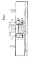
- the device shown in Figure 1 consists of a vacuum chamber 2, in which a substrate 3 is held and guided longitudinally displaceable, wherein above the substrate 3, a diaphragm 4 is provided with aperture 5, the precipitate of the atomized from the target 6 of the cathode 7 material the surface of the moving in the direction of arrow A substrate 3 is allowed.
- the cathode 7 is connected via a line 9 to a DC power source 8 and is otherwise separated by means of a cup-shaped housing 10 of the compartments 11 and 12, in each of which cathodes 13,14 are arranged, whose targets 15,16 respectively to the lower Wall portion 17 and 18 of the compartments 11,12 are aligned.
- the cathodes 13, 14 are each connected to a pole 20 or 21 of the alternating current source 19 via a respective current conductor 22, 23.
- gas supply lines 24,25 with nozzles 26,27 via the process gas into the gap 28, which is bounded by the target 6 on the one hand and the substrate 3 on the other hand, flows.
- the electrical conductors 22,23 are each connected via a resistor with diode 29,30 with the vacuum chamber 2 and the vacuum chamber 2 is also connected to vacuum pumps 31,32, and that in the plane of the target. 6 the diode cathode 7 gaps or openings 33 and 34 are provided, which connect the compartments 11,12 with the space 35 immediately in front of the target 6, so that the plasma generated by the magnetron cathodes 13,14 uniformly in front of the target Diode cathode (the cathode without magnet assembly) 7 in the room 35 burns. Further openings 35,36 in the outer walls of the compartments 11,12 allow the rapid evacuation of these compartments.
- the embodiment according to Figure 2 differs from that of Figure 1 in that the magnetron cathodes 13,14 are aligned so that their targets 15,16 the outer walls 37,38 of the compartments 11,12 are opposite.
- FIG. 3 differs from that of Figure 1 essentially in that the compartments 11,12 via rear openings or channels 39,40 in the walls 41,42, which face each other, communicate with each other.
- the TwinMag cathodes 13, 14 (arrangement of two magnetron cathodes) are equipped with a target 15, 16 made of carbon in order to obtain the lowest possible sputtering rate, because in this arrangement the sputtering effect of the magnetron discharge is undesirable.
- the diode cathode 7 is covered with a target 6, which contains the material to be sputtered. All three cathodes are in a vacuum chamber 2. The three cathodes each have a dark space shield. The dark space shields of the TwinMag cathodes are floating while the dark space shield of the diode cathode is grounded.
- the diode cathode 7 is connected to a DC power supply, wherein the positive pole of the power supply is connected to the vacuum chamber, that is grounded.
- the AC voltage (AC line voltage or center frequency or a frequency in between) is applied to the two TwinMag cathodes 13,14. Due to the alternating voltage, a plasma band develops between the two cathodes 13, 14. The spread of the plasma band is limited by the shielding of the device, so that the plasma band passes over the target of the diode cathode.
- the gas inlet is located below said shield so that the targets can not be struck directly by a gas jet.
Landscapes
- Engineering & Computer Science (AREA)
- Physics & Mathematics (AREA)
- Plasma & Fusion (AREA)
- Chemical & Material Sciences (AREA)
- Analytical Chemistry (AREA)
- Manufacturing & Machinery (AREA)
- Physical Vapour Deposition (AREA)
Claims (3)
- Dispositif de revêtement d'un substrat (3) par des cibles (15, 16) électriquement conductrices, ledit dispositif comportant une source de courant alternatif (19) qui est reliée à deux cathodes de magnétron (13, 14) qui coopèrent électriquement avec les cibles (15, 16), un pôle (20) de la source de courant alternatif (19) étant raccordé à une cathode (13) et l'autre pôle (21) étant raccordé à l'autre cathode (14) par des lignes d'alimentation (22, 23), caractérisé en ce que chacune des deux cathodes de magnétron (13, 14) est disposée dans un propre compartiment (11, 12) à l'intérieur de la chambre à dépression (2) et les deux compartiments (11, 12) sont reliés par des fentes (33, 34) ou des ouvertures, ménagées dans leur paroi de séparation, à un troisième compartiment (1) ou à une région (35) se trouvant juste en avant de ce troisième compartiment (1), une cathode de diode (7) dotée d'une cible de pulvérisation (6) étant placée dans le troisième compartiment (1) et étant raccordée par une ligne (9) à une alimentation propre en courant continu (8), et des conduites de gaz (24, 25) débouchant dans l'espace (28) situé entre la cathode de diode (7) et le plan de substrat (3) situé en face de cette cathode de diode et permettant d'introduire le gaz de traitement dans cette région (28) située entre la cible (6) de la cathode de diode (7) et le substrat (3).
- Dispositif selon la revendication 1, caractérisé en outre en ce que les cathodes de magnétron (13, 14) sont orientées de telle sorte que les plans de leurs cibles (15, 16) s'étendent parallèlement aux pièces de fond (17, 18) situées en face du plan de substrat ou en ce que les plans de leurs cibles (15, 16) s'étendent parallèlement aux parois latérales (37, 38) destinées à limiter vers l'extérieur les compartiments (11, 12).
- Dispositif selon les revendications 1 et 2, caractérisé en outre en ce que les deux compartiments (11, 12), contenant les cathodes de magnétron (13, 14), sont entourés par une chambre à dépression (2), et en ce que les pièces de fond (17, 18) des compartiments (11, 12) s'étendent dans un plan qui est parallèle au plan de la cible (6) de la cathode de diode (7) et parallèle au plan de substrat (3), et les deux fentes ou ouvertures (33, 34) destinées à la sortie du flux de plasma sont ménagées, en étant diamétralement opposées, dans les parois latérales (41, 42) des compartiments et se trouvent dans un plan situé au-dessous du plan de la cible (6) de la cathode de diode (7).
Applications Claiming Priority (2)
| Application Number | Priority Date | Filing Date | Title |
|---|---|---|---|
| DE19540794 | 1995-11-02 | ||
| DE19540794A DE19540794A1 (de) | 1995-11-02 | 1995-11-02 | Vorrichtung zum Beschichten eines Substrats von einem elektrisch leitfähigen Target |
Publications (3)
| Publication Number | Publication Date |
|---|---|
| EP0772223A2 EP0772223A2 (fr) | 1997-05-07 |
| EP0772223A3 EP0772223A3 (fr) | 2004-11-10 |
| EP0772223B1 true EP0772223B1 (fr) | 2007-01-03 |
Family
ID=7776415
Family Applications (1)
| Application Number | Title | Priority Date | Filing Date |
|---|---|---|---|
| EP96111817A Expired - Lifetime EP0772223B1 (fr) | 1995-11-02 | 1996-07-23 | Dispositif pour revêtir un substrat à partir de cibles conductrices d'électricité |
Country Status (6)
| Country | Link |
|---|---|
| US (1) | US5718815A (fr) |
| EP (1) | EP0772223B1 (fr) |
| JP (1) | JP3995062B2 (fr) |
| KR (1) | KR100210268B1 (fr) |
| DE (2) | DE19540794A1 (fr) |
| TW (1) | TW328608B (fr) |
Families Citing this family (19)
| Publication number | Priority date | Publication date | Assignee | Title |
|---|---|---|---|---|
| DE19506515C1 (de) * | 1995-02-24 | 1996-03-07 | Fraunhofer Ges Forschung | Verfahren zur reaktiven Beschichtung |
| EP0783174B1 (fr) * | 1995-10-27 | 2006-12-13 | Applied Materials GmbH & Co. KG | Dispositif pour le revêtement d'un substrat |
| DE19644752A1 (de) * | 1996-10-28 | 1998-04-30 | Leybold Systems Gmbh | Interferenzschichtensystem |
| DE19651378A1 (de) * | 1996-12-11 | 1998-06-18 | Leybold Systems Gmbh | Vorrichtung zum Aufstäuben von dünnen Schichten auf flache Substrate |
| DE19733940C2 (de) * | 1997-08-06 | 2001-03-01 | Leybold Systems Gmbh | Vorrichtung zum Beschichten von plattenförmigen Substraten mit dünnen Schichten mittels Kathodenzerstäubung |
| DE19741708A1 (de) * | 1997-09-22 | 1999-04-01 | Leybold Systems Gmbh | Vorrichtung zum Aufbringen dünner Schichten auf ein Substrat |
| DE29717418U1 (de) * | 1997-09-26 | 1998-01-22 | Leybold Systems GmbH, 63450 Hanau | Vorrichtung zum Aufbringen dünner Schichten auf ein Substrat |
| DE19813075A1 (de) * | 1998-03-25 | 1999-09-30 | Leybold Ag | Vorrichtung zum Beschichten eines Substrates |
| US6620298B1 (en) * | 1999-04-23 | 2003-09-16 | Matsushita Electric Industrial Co., Ltd. | Magnetron sputtering method and apparatus |
| US7411352B2 (en) * | 2002-09-19 | 2008-08-12 | Applied Process Technologies, Inc. | Dual plasma beam sources and method |
| DE10352143B4 (de) | 2003-11-04 | 2009-06-25 | Von Ardenne Anlagentechnik Gmbh | Längserstreckte Vakuumanlage zur ein- oder beidseitigen Beschichtung flacher Substrate |
| KR200377696Y1 (ko) * | 2004-12-03 | 2005-03-11 | 동 호 김 | 후레쉬기능을 가지는 리모콘 |
| US20100252419A1 (en) * | 2009-02-02 | 2010-10-07 | Klaus Bollmann | Method of manufacturing a high density capacitor or other microscopic layered mechanical device |
| JP6092721B2 (ja) * | 2013-06-21 | 2017-03-08 | 株式会社アルバック | 成膜装置 |
| EP3648551B1 (fr) | 2017-06-27 | 2021-08-18 | Canon Anelva Corporation | Dispositif de traitement par plasma |
| TWI745813B (zh) | 2017-06-27 | 2021-11-11 | 日商佳能安內華股份有限公司 | 電漿處理裝置 |
| KR102257134B1 (ko) | 2017-06-27 | 2021-05-26 | 캐논 아네르바 가부시키가이샤 | 플라스마 처리 장치 |
| SG11201912566WA (en) | 2017-06-27 | 2020-01-30 | Canon Anelva Corp | Plasma processing apparatus |
| CN112292911A (zh) * | 2018-06-26 | 2021-01-29 | 佳能安内华股份有限公司 | 等离子体处理装置、等离子体处理方法、程序和存储介质 |
Family Cites Families (14)
| Publication number | Priority date | Publication date | Assignee | Title |
|---|---|---|---|---|
| DE252205C (fr) | ||||
| US4629548A (en) * | 1985-04-03 | 1986-12-16 | Varian Associates, Inc. | Planar penning magnetron sputtering device |
| DE3541621A1 (de) | 1985-11-25 | 1987-05-27 | Siemens Ag | Anordnung zum abscheiden einer metallegierung |
| JPH01158644A (ja) * | 1987-12-14 | 1989-06-21 | Matsushita Electric Ind Co Ltd | 光磁気記録担体の製造装置 |
| DE3802852A1 (de) | 1988-02-01 | 1989-08-03 | Leybold Ag | Einrichtung fuer die beschichtung eines substrats mit einem material, das aus einem plasma gewonnen wird |
| US4911814A (en) * | 1988-02-08 | 1990-03-27 | Nippon Telegraph And Telephone Corporation | Thin film forming apparatus and ion source utilizing sputtering with microwave plasma |
| JPH01268869A (ja) * | 1988-04-20 | 1989-10-26 | Fuji Photo Film Co Ltd | スパッタリング装置 |
| JPH0826453B2 (ja) * | 1988-12-26 | 1996-03-13 | 富士写真フイルム株式会社 | スパッタリング装置 |
| DE4106770C2 (de) | 1991-03-04 | 1996-10-17 | Leybold Ag | Verrichtung zum reaktiven Beschichten eines Substrats |
| DE4120690A1 (de) * | 1991-06-22 | 1992-12-24 | Leybold Ag | Targetvorrichtung aus ferromagnetischem material fuer eine magnetron-elektrode |
| US5415757A (en) * | 1991-11-26 | 1995-05-16 | Leybold Aktiengesellschaft | Apparatus for coating a substrate with electrically nonconductive coatings |
| DE4204999A1 (de) | 1991-11-26 | 1993-08-26 | Leybold Ag | Verfahren und vorrichtung zum beschichten eines substrats, insbesondere mit elektrisch nichtleitenden schichten |
| DE4237517A1 (de) * | 1992-11-06 | 1994-05-11 | Leybold Ag | Vorrichtung zum Beschichten eines Substrats, insbesondere mit elektrisch nichtleitenden Schichten |
| DE4326100B4 (de) * | 1993-08-04 | 2006-03-23 | Unaxis Deutschland Holding Gmbh | Verfahren und Vorrichtung zum Beschichten von Substraten in einer Vakuumkammer, mit einer Einrichtung zur Erkennung und Unterdrückung von unerwünschten Lichtbögen |
-
1995
- 1995-11-02 DE DE19540794A patent/DE19540794A1/de not_active Withdrawn
-
1996
- 1996-07-23 DE DE59611407T patent/DE59611407D1/de not_active Expired - Lifetime
- 1996-07-23 EP EP96111817A patent/EP0772223B1/fr not_active Expired - Lifetime
- 1996-08-10 TW TW085109722A patent/TW328608B/zh not_active IP Right Cessation
- 1996-09-12 US US08/711,885 patent/US5718815A/en not_active Expired - Lifetime
- 1996-10-23 KR KR1019960047632A patent/KR100210268B1/ko not_active Expired - Lifetime
- 1996-11-01 JP JP29167796A patent/JP3995062B2/ja not_active Expired - Lifetime
Also Published As
| Publication number | Publication date |
|---|---|
| JP3995062B2 (ja) | 2007-10-24 |
| DE59611407D1 (de) | 2007-02-15 |
| DE19540794A1 (de) | 1997-05-07 |
| US5718815A (en) | 1998-02-17 |
| KR100210268B1 (ko) | 1999-07-15 |
| EP0772223A2 (fr) | 1997-05-07 |
| KR970030004A (ko) | 1997-06-26 |
| EP0772223A3 (fr) | 2004-11-10 |
| TW328608B (en) | 1998-03-21 |
| JPH09170078A (ja) | 1997-06-30 |
Similar Documents
| Publication | Publication Date | Title |
|---|---|---|
| EP0772223B1 (fr) | Dispositif pour revêtir un substrat à partir de cibles conductrices d'électricité | |
| DE19651811B4 (de) | Vorrichtung zum Belegen eines Substrats mit dünnen Schichten | |
| EP0593924B1 (fr) | Dispositif pour la production d'un plasma au moyen d'une pulvérisation cathodique | |
| EP0205028B1 (fr) | Appareil pour le dépôt de couches minces sur un substrat | |
| DE3920835C2 (de) | Einrichtung zum Beschichten von Substraten | |
| EP0783174B1 (fr) | Dispositif pour le revêtement d'un substrat | |
| DE3854276T2 (de) | Kathodenzerstäubungsverfahren und Vorrichtung zur Durchführung desselben. | |
| EP0502242B1 (fr) | Dispositif pour pulverisation réactif | |
| DE69814687T2 (de) | Plasmavorrichtung mit einem mit einer spannungsquelle verbundenen metallteil, das zwischen einer rf-plasma-anregungsquelle und dem plasma angeordnet ist | |
| DE19540543A1 (de) | Vorrichtung zum Beschichten eines Substrats mit Hilfe des Chemical-Vapor-Deposition-Verfahrens | |
| EP3309815B1 (fr) | Dispositif de traitement au plasma comprenant deux sources de plasma excitées par micro-ondes couplées ensemble et procédé de fonctionnement d'un tel dispositif de traitement au plasma | |
| DE69009078T2 (de) | System und Methode zur Ablagerung von dünnen Filmen im Vakuum. | |
| DE19651378A1 (de) | Vorrichtung zum Aufstäuben von dünnen Schichten auf flache Substrate | |
| EP0755461A1 (fr) | Procede et dispositif de revetement par evaporation sous vide par voie ionique | |
| DE112009001457T5 (de) | Sputter-Vorrichtung | |
| DE3802852C2 (fr) | ||
| EP2585622A1 (fr) | Source d'évaporation par arc présentant un champ électrique défini | |
| DE19939040B4 (de) | Magnetronsputtergerät | |
| DE4336830A1 (de) | Plasma-Zerstäubungsanlage mit Mikrowellenunterstützung | |
| EP0775758A1 (fr) | Appareillage de revêtement sous vide avec un creuset pour recevoir le matériau à évaporer dans la chambre à vide | |
| DE3226717C2 (fr) | ||
| EP0811238B1 (fr) | Dispositif de pulverisation reactive | |
| DE68909262T2 (de) | Vorrichtung für RF-Plasma-Verarbeitung. | |
| DE4230290A1 (de) | Vorrichtung zum Erzeugen eines Plasmas mittels Kathodenzerstäubung und Mikrowelleneinstrahlung | |
| DE4138793C2 (de) | Verfahren und Vorrichtung zum Beschichten eines Substrats, insbesondere mit elektrisch nichtleitenden Schichten |
Legal Events
| Date | Code | Title | Description |
|---|---|---|---|
| PUAI | Public reference made under article 153(3) epc to a published international application that has entered the european phase |
Free format text: ORIGINAL CODE: 0009012 |
|
| AK | Designated contracting states |
Kind code of ref document: A2 Designated state(s): BE CH DE ES FR GB IT LI LU NL SE |
|
| PUAL | Search report despatched |
Free format text: ORIGINAL CODE: 0009013 |
|
| AK | Designated contracting states |
Kind code of ref document: A3 Designated state(s): BE CH DE ES FR GB IT LI LU NL SE |
|
| RAP1 | Party data changed (applicant data changed or rights of an application transferred) |
Owner name: UNAXIS DEUTSCHLAND HOLDING GMBH |
|
| 17P | Request for examination filed |
Effective date: 20050504 |
|
| GRAP | Despatch of communication of intention to grant a patent |
Free format text: ORIGINAL CODE: EPIDOSNIGR1 |
|
| RTI1 | Title (correction) |
Free format text: DEVICE FOR COATING A SUBSTRATE FROM ELECTRICALLY CONDUCTIVE TARGETS |
|
| GRAS | Grant fee paid |
Free format text: ORIGINAL CODE: EPIDOSNIGR3 |
|
| RAP1 | Party data changed (applicant data changed or rights of an application transferred) |
Owner name: UNAXIS DEUTSCHLAND HOLDING GMBH |
|
| RAP1 | Party data changed (applicant data changed or rights of an application transferred) |
Owner name: OERLIKON DEUTSCHLAND HOLDING GMBH |
|
| GRAA | (expected) grant |
Free format text: ORIGINAL CODE: 0009210 |
|
| AK | Designated contracting states |
Kind code of ref document: B1 Designated state(s): BE CH DE ES FR GB IT LI LU NL SE |
|
| REG | Reference to a national code |
Ref country code: GB Ref legal event code: FG4D Free format text: NOT ENGLISH |
|
| GBT | Gb: translation of ep patent filed (gb section 77(6)(a)/1977) |
Effective date: 20070105 |
|
| REF | Corresponds to: |
Ref document number: 59611407 Country of ref document: DE Date of ref document: 20070215 Kind code of ref document: P |
|
| PG25 | Lapsed in a contracting state [announced via postgrant information from national office to epo] |
Ref country code: SE Free format text: LAPSE BECAUSE OF FAILURE TO SUBMIT A TRANSLATION OF THE DESCRIPTION OR TO PAY THE FEE WITHIN THE PRESCRIBED TIME-LIMIT Effective date: 20070403 |
|
| PG25 | Lapsed in a contracting state [announced via postgrant information from national office to epo] |
Ref country code: ES Free format text: LAPSE BECAUSE OF FAILURE TO SUBMIT A TRANSLATION OF THE DESCRIPTION OR TO PAY THE FEE WITHIN THE PRESCRIBED TIME-LIMIT Effective date: 20070414 |
|
| ET | Fr: translation filed | ||
| PLBE | No opposition filed within time limit |
Free format text: ORIGINAL CODE: 0009261 |
|
| STAA | Information on the status of an ep patent application or granted ep patent |
Free format text: STATUS: NO OPPOSITION FILED WITHIN TIME LIMIT |
|
| 26N | No opposition filed |
Effective date: 20071005 |
|
| BERE | Be: lapsed |
Owner name: OERLIKON DEUTSCHLAND HOLDING G.M.B.H. Effective date: 20070731 |
|
| PG25 | Lapsed in a contracting state [announced via postgrant information from national office to epo] |
Ref country code: BE Free format text: LAPSE BECAUSE OF NON-PAYMENT OF DUE FEES Effective date: 20070731 |
|
| PG25 | Lapsed in a contracting state [announced via postgrant information from national office to epo] |
Ref country code: LU Free format text: LAPSE BECAUSE OF NON-PAYMENT OF DUE FEES Effective date: 20070723 |
|
| REG | Reference to a national code |
Ref country code: FR Ref legal event code: PLFP Year of fee payment: 20 |
|
| PGFP | Annual fee paid to national office [announced via postgrant information from national office to epo] |
Ref country code: FR Payment date: 20150626 Year of fee payment: 20 |
|
| PGFP | Annual fee paid to national office [announced via postgrant information from national office to epo] |
Ref country code: NL Payment date: 20150721 Year of fee payment: 20 |
|
| PGFP | Annual fee paid to national office [announced via postgrant information from national office to epo] |
Ref country code: CH Payment date: 20150721 Year of fee payment: 20 Ref country code: DE Payment date: 20150721 Year of fee payment: 20 Ref country code: GB Payment date: 20150721 Year of fee payment: 20 |
|
| PGFP | Annual fee paid to national office [announced via postgrant information from national office to epo] |
Ref country code: IT Payment date: 20150729 Year of fee payment: 20 |
|
| REG | Reference to a national code |
Ref country code: DE Ref legal event code: R071 Ref document number: 59611407 Country of ref document: DE |
|
| REG | Reference to a national code |
Ref country code: NL Ref legal event code: MK Effective date: 20160722 |
|
| REG | Reference to a national code |
Ref country code: CH Ref legal event code: PL |
|
| REG | Reference to a national code |
Ref country code: GB Ref legal event code: PE20 Expiry date: 20160722 |
|
| PG25 | Lapsed in a contracting state [announced via postgrant information from national office to epo] |
Ref country code: GB Free format text: LAPSE BECAUSE OF EXPIRATION OF PROTECTION Effective date: 20160722 |