EP0773549A2 - Synchroner Halbleiterspeicher mit einem systemzyklusabhängigen Schreibausführungszyklus - Google Patents
Synchroner Halbleiterspeicher mit einem systemzyklusabhängigen Schreibausführungszyklus Download PDFInfo
- Publication number
- EP0773549A2 EP0773549A2 EP96118057A EP96118057A EP0773549A2 EP 0773549 A2 EP0773549 A2 EP 0773549A2 EP 96118057 A EP96118057 A EP 96118057A EP 96118057 A EP96118057 A EP 96118057A EP 0773549 A2 EP0773549 A2 EP 0773549A2
- Authority
- EP
- European Patent Office
- Prior art keywords
- write
- signal
- synchronous signal
- receiving
- semiconductor memory
- Prior art date
- Legal status (The legal status is an assumption and is not a legal conclusion. Google has not performed a legal analysis and makes no representation as to the accuracy of the status listed.)
- Granted
Links
- 230000001360 synchronised effect Effects 0.000 title claims abstract description 112
- 239000004065 semiconductor Substances 0.000 title claims abstract description 47
- 230000036962 time dependent Effects 0.000 title 1
- 239000000872 buffer Substances 0.000 claims description 8
- 201000008103 leukocyte adhesion deficiency 3 Diseases 0.000 description 19
- 230000004044 response Effects 0.000 description 12
- 230000000630 rising effect Effects 0.000 description 10
- 238000010586 diagram Methods 0.000 description 8
- 238000000034 method Methods 0.000 description 8
- 230000008569 process Effects 0.000 description 8
- 101100539927 Saccharomyces cerevisiae (strain ATCC 204508 / S288c) NAN1 gene Proteins 0.000 description 5
- 102100035606 Beta-casein Human genes 0.000 description 4
- 101150110971 CIN7 gene Proteins 0.000 description 4
- 101000947120 Homo sapiens Beta-casein Proteins 0.000 description 4
- 101150110298 INV1 gene Proteins 0.000 description 4
- 101100397044 Xenopus laevis invs-a gene Proteins 0.000 description 4
- 238000004519 manufacturing process Methods 0.000 description 4
- HCUOEKSZWPGJIM-YBRHCDHNSA-N (e,2e)-2-hydroxyimino-6-methoxy-4-methyl-5-nitrohex-3-enamide Chemical compound COCC([N+]([O-])=O)\C(C)=C\C(=N/O)\C(N)=O HCUOEKSZWPGJIM-YBRHCDHNSA-N 0.000 description 3
- 101001109689 Homo sapiens Nuclear receptor subfamily 4 group A member 3 Proteins 0.000 description 3
- 101000598778 Homo sapiens Protein OSCP1 Proteins 0.000 description 3
- 101001067395 Mus musculus Phospholipid scramblase 1 Proteins 0.000 description 3
- 102100022673 Nuclear receptor subfamily 4 group A member 3 Human genes 0.000 description 3
- 230000001965 increasing effect Effects 0.000 description 3
- 230000009471 action Effects 0.000 description 2
- 238000013459 approach Methods 0.000 description 2
- 230000002950 deficient Effects 0.000 description 2
- 230000000694 effects Effects 0.000 description 2
- 230000004048 modification Effects 0.000 description 2
- 238000012986 modification Methods 0.000 description 2
- 238000005457 optimization Methods 0.000 description 2
- 230000003213 activating effect Effects 0.000 description 1
- 230000007547 defect Effects 0.000 description 1
- 230000001934 delay Effects 0.000 description 1
- 238000009792 diffusion process Methods 0.000 description 1
- 230000003028 elevating effect Effects 0.000 description 1
- 230000002401 inhibitory effect Effects 0.000 description 1
- 238000004904 shortening Methods 0.000 description 1
Images



Classifications
-
- G—PHYSICS
- G11—INFORMATION STORAGE
- G11C—STATIC STORES
- G11C7/00—Arrangements for writing information into, or reading information out from, a digital store
- G11C7/22—Read-write [R-W] timing or clocking circuits; Read-write [R-W] control signal generators or management
-
- G—PHYSICS
- G11—INFORMATION STORAGE
- G11C—STATIC STORES
- G11C11/00—Digital stores characterised by the use of particular electric or magnetic storage elements; Storage elements therefor
- G11C11/21—Digital stores characterised by the use of particular electric or magnetic storage elements; Storage elements therefor using electric elements
- G11C11/34—Digital stores characterised by the use of particular electric or magnetic storage elements; Storage elements therefor using electric elements using semiconductor devices
- G11C11/40—Digital stores characterised by the use of particular electric or magnetic storage elements; Storage elements therefor using electric elements using semiconductor devices using transistors
- G11C11/401—Digital stores characterised by the use of particular electric or magnetic storage elements; Storage elements therefor using electric elements using semiconductor devices using transistors forming cells needing refreshing or charge regeneration, i.e. dynamic cells
-
- G—PHYSICS
- G11—INFORMATION STORAGE
- G11C—STATIC STORES
- G11C7/00—Arrangements for writing information into, or reading information out from, a digital store
- G11C7/10—Input/output [I/O] data interface arrangements, e.g. I/O data control circuits, I/O data buffers
- G11C7/1072—Input/output [I/O] data interface arrangements, e.g. I/O data control circuits, I/O data buffers for memories with random access ports synchronised on clock signal pulse trains, e.g. synchronous memories, self timed memories
Definitions
- the present invention relates to a semiconductor memory, and more specifically to a write control circuit for use in a synchronous semiconductor memory.
- This synchronous semiconductor memory having the internal pipeline structure is featured in that, at the time of reading, an address access path is divided into a plurality of stages, and the reading is carried out in a time-division manner, so that a cycle time is shortened. Therefore, at the time of writing, it is necessary to write data into a sense amplifier during the shortened cycle time.
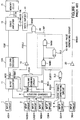
- FIG. 1 there is shown a block diagram illustrating one example of the prior art synchronous semiconductor memory.
- An input section of the shown semiconductor memory includes a plurality of input circuits connected to receive a plurality of bits of an input address ADD. These input circuits are represented by only one input circuit 1 for simplification of drawing.
- the input section also includes a plurality of input circuits 2 to 5 connected to receive a plurality of control signals RASB, CASB, WEB and CSB, respectively, an input circuit 6 connected to receive an external clock CLK, and an input circuit 7 connected to receive data DQ from a data input/output terminal.
- An internal circuit of the shown semiconductor memory includes a synchronous signal generating circuit 8 connected to an output of the input circuit 6 for generating a synchronous signal ICLK1, a delay DL3 receiving the synchronous signal ICLK1 for generating another synchronous signal ICLK1D by delaying the received synchronous signal ICLK1 by a predetermined constant time, a command decoder 9 connected to receive outputs of the input circuits 2 to 5, for generating a read enable signal REN and a write enable signal WEN in synchronism with the synchronous signal ICLK1, and a pipeline enabling circuit 10 receiving the read enable signal REN, the write enable signal WEN and a burst end signal BSTEND explained hereinafter, for generating a pipeline enable signal PEN.
- a synchronous signal generating circuit 8 connected to an output of the input circuit 6 for generating a synchronous signal ICLK1, a delay DL3 receiving the synchronous signal ICLK1 for generating another synchronous signal ICLK1D by delaying the received synchronous signal
- the internal circuit of the shown semiconductor memory also includes a burst counter 11 receiving an output of the input circuit 1, the pipeline enable signal PEN and the synchronous signal ICLK1, for generating a plurality of internal address signals IADD, plate selection signals PSEL1 and the above mentioned burst end signal BSTEND, a column decoder 12A receiving the plurality of internal address signals IADD, and having outputs connected to a plurality of column selection lines YSW, a buffer 19 receiving the plate selection signals PSEL1 for outputting plate selection signals PSEL2, another buffer 20 receiving an output of the input circuit 7 for outputting a write data to a write bus WBUS1, a write pulse generating circuit 13 receiving the pipeline enable signal PEN, the write enable signal WEN and the synchronous signal ICLK1, for generating a write pulse WP, an AND gate AN receiving the plate selection signals PSEL2 and the write pulse WP, for generating a write switch signal WSW, a write buffer 14 receiving the write switch signal WSW and the write bus WBUS1, for supplying
- the write pulse generating circuit 13 includes a NAND gate NAN3 receiving the pipeline enable signal PEN, the write enable signal WEN and the synchronous signal ICLK1, a delay DL4 receiving an output of the NAND gate NAN3 for generating a signal by delaying the received signal by a predetermined constant time, and a NAND gate NAN4 receiving the output of the NAND gate NAN3 and an output of the delay DL4, for outputting the write pulse WP.
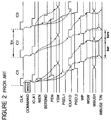
- Figure 2 is a timing chart illustrating an operation of the prior art synchronous semiconductor memory.
- the command decoder 9 brings the write enable signal WEN to a high level in response to the synchronous signal ICLK1 which assumes a high level in response to the external clock CLK. Accordingly, the pipeline enable signal PEN is also brought to the high level by the pipeline enable circuit 10.
- the burst counter 11 If the write command is inputted, the burst counter 11 generates an internal address IADD for a separately set "burst length".
- the internal address IADD for the separately set "burst length" (2 bits) is generated in cycles C1 nd C2 by the burst counter 11, and then, a high level pulse is generated as the burst end signal BSTEND by the burst counter 11 in response to a rising of the synchronous signal ICLK1 of a cycle C3.
- the pipeline enable circuit 10 brings the pipeline enable signal PEN to a low level.
- the plate selection signal PSEL1 and the internal address IADD (not shown in Figure 2) are generated and the column decoder 12A receiving the internal address IADD selects one of the column selection lines YSW.
- the plate selection signals PSEL1 are not changed in the cycle C2, but the selected line of the column selection lines YSW is changed for each cycle.
- the content of the plate selection signals PSEL1 are transferred as the plate selection signals PSEL2, and a write data is transferred to the write bus WBUS1.
- the write pulse WP is similarly generated, but during the cycle C3, the write pulse WP is maintained at the low level, because the pipeline enable signal PEN is brought to the low level before the synchronous signal ICLK1D is brought to the high level, and therefore, the output of the NAND gate NAN3 remains at the high level.
- the write data is transferred to the write bus pairs WBUS2 T/N when the write switch signal WSW (which is generated in response to the write pulse WP during a period that the plate selection signal PSEL2 is at the high level) is at the high level.
- the rising timing of the synchronous signal ICLK1D is determined by adjusting the delay amount of the delay DL3 to the effect that the write switch signal WSW is brought to the high level after the column selection lines YSW, the plate selection signals PSEL2 and the write bus WBUS1 are changed, and if the delay amount of the delay DL4 is adjusted to ensure that the write switch signal WSW is brought to the low level after data has been accurately written into the sense amplifier 16.
- the write execution time namely, the high level width of the write pulse WP is determined by the delay amount of the delay DL4.
- the write execution time is t WP and the cycle time is t CK
- the cycle time t CK is expressed as follows: t CK > t WP + t WPBmin
- FIG 3 there is shown a timing chart illustrating an operation of the prior art synchronous semiconductor memory in the case that the cycle time t CK is long.
- the write execution time t WP is the same as that of the example shown in Figure 2. Namely, the write execution time t WP is constant independently of the cycle time t CK .
- the required write execution time t WP is different from one semiconductor memory to another because of a manufacturing process variation. Accordingly, it is necessary to determine the delay amount of the delay DL4 and to set the write execution time t WP , with a margin which makes it possible to perform an accurate writing in most of devices.
- the write execution time t WP is set to meet with devices manufactured under the process condition which needs the longest write execution time, by taking the manufacturing process variation into consideration.
- the write execution time t WP becomes longer than a required time, which results in an unnecessarily long cycle time t CK .
- all of devices have the same long cycle time t CK as that of the devices manufactured under the process condition which needs the longest write execution time.
- the cycle time for the reading is being speeded up, and therefore, the speed grade is often determined by the cycle time for the writing. In the above mentioned situation, only devices having a low speed grade can be manufactured.
- JP-A-4-243085 which corresponds to U.S. Patent 5,293,347, proposes to provide two write buffers or drivers for one sense amplifier.
- the disclosure of these publications is incorporated by reference in their entirety into this application.
- Another object of the present invention is to provide a synchronous semiconductor memory capable of shortening the cycle time for the writing.
- a semiconductor memory comprising a plurality of memory cells, a plurality of sense amplifiers connected through digit lines to the memory cells, and a write control means receiving a synchronous signal generated on the basis of an external clock, for generating a write switch signal for controlling a writing of data to the sense amplifiers, the write control means maintaining the write switch signal in an inactive condition until a first timing after at least a first predetermined delay time from the synchronous signal, and bringing the write switch signal into an active condition at a second timing after a second predetermined delay time from the first timing, the write control means maintaining the write switch signal in the active condition until a synchronous signal next to the synchronous signal is generated.
- the write control means includes a pulse generating circuit receiving the internal synchronous signal for generating a pulse starting from the first timing and having a pulse width corresponding to a difference between the first timing and the second timing, and a logic gate means receiving a plate selection signal and the pulse, for generating the write switch signal which is maintained in the inactive condition until the first timing firstly appearing after the logic gate means receives the plate selection signal.
- the semiconductor memory further includes means for switching a plurality of column selection lines connected to the sense amplifiers, after the first timing but before the second timing.
- the semiconductor memory further includes a synchronous signal generating circuit receiving the external clock for generating a first internal synchronous signal in synchronism with the external clock, and a delay means receiving the first internal synchronous signal for generating a second internal synchronous signal by delaying the first internal synchronous signal.
- the write control means brings the write switch signal into the inactive condition in synchronism with the second internal synchronous signal, and the column selection signal is switched in synchronism with the second internal synchronous signal.
- the semiconductor memory further includes a write buffer receiving the write switch signal and a first write bus for transferring a write data, and connected through a second write bus to the plurality of sense amplifiers, and a latch means connected to receive the write data from an external and having an output connected to the first write bus, the latch means updating the write data on the first write bus in synchronism with the second internal synchronous signal.
- another latch means receiving the plate selection signal for outputting the plate selection signal latched in the latch means, the latch means updating the latched plate selection signal in synchronism with the second internal synchronous signal.
- the semiconductor memory further includes a command decoder receiving a plurality of control signals from an external, for generating a write enable signal, a pipeline enabling circuit receiving at least the write enable signal, for generating a pipeline enable signal, a write mask control means receiving a data mask command from the external, for generating a write mask control signal, and a write pulse generating circuit receiving the write enable signal, the pipeline enable signal, the write mask control signal, and the synchronous signal, for maintaining the write switch signal in the inactive condition when at least one of the write enable signal and the pipeline enable signal is inactive, or when the write mask control signal is active.
- a command decoder receiving a plurality of control signals from an external, for generating a write enable signal
- a pipeline enabling circuit receiving at least the write enable signal, for generating a pipeline enable signal
- a write mask control means receiving a data mask command from the external, for generating a write mask control signal
- a write pulse generating circuit receiving the write enable signal, the pipeline enable signal, the write mask control
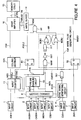
- FIG 4 there is shown a block diagram of a first embodiment of the synchronous semiconductor memory in accordance with the present invention.
- elements corresponding to those shown in Figure 1 are given the same Reference Numerals.
- an input section of the shown first embodiment of the synchronous semiconductor memory in accordance with the present invention includes a plurality of input circuits connected to receive a plurality of bits of an input address ADD. These input circuits are represented by only one input circuit 1 for simplification of drawing.
- the input section also includes a plurality of input circuits 2 to 5 connected to receive a plurality of control signals RASB, CASB, WEB and CSB, respectively, an input circuit 6 connected to receive an external clock CLK, and an input circuit 7 connected to receive data DQ from a data input/output terminal.
- An internal circuit of the shown embodiment includes a synchronous signal generating circuit 8 connected to an output of the input circuit 6 for generating an internal synchronous signal ICLK1, a delay DL1 receiving the internal synchronous signal ICLK1 for generating another internal synchronous signal ICLK1D by delaying the received synchronous signal ICLK1 by a predetermined constant time, a command decoder 9 connected to receive outputs of the input circuits 2 to 5, for generating a read enable signal REN and a write enable signal WEN in synchronism with the internal synchronous signal ICLK1, and a pipeline enabling circuit 10 receiving the read enable signal REN, the write enable signal WEN and a burst end signal BSTEND explained hereinafter, for generating a pipeline enable signal PEN.
- a synchronous signal generating circuit 8 connected to an output of the input circuit 6 for generating an internal synchronous signal ICLK1, a delay DL1 receiving the internal synchronous signal ICLK1 for generating another internal synchronous signal ICLK1D by delaying the
- the internal circuit of the shown embodiment also includes a burst counter 11 receiving an output of the input circuit 1, the pipeline enable signal PEN and the internal synchronous signal ICLK1, for generating a plurality of internal address signals IADD, a plurality of plate selection signals PSEL1 and the above mentioned burst end signal BSTEND (the internal address signals IADD and the plate selection signals PSEL1 are represented by only one line for simplification of drawing), a column decoder 12A receiving the plurality of internal address signals IADD, and having outputs connected to a plurality of column selection lines YSW (which are represented by only one line for simplification of drawing), a plurality of D-latches (which are represented by only one D-latch R1 for simplification of drawing) each receiving a corresponding one of the plate selection signals PSEL1 for outputting a plate selection signals PSEL2 in synchronism with the internal synchronous signal ICLK1D.
- a burst counter 11 receiving an output of the input circuit 1, the pipeline enable signal PEN and the internal synchronous
- the internal circuit of the shown embodiment includes a plurality of D-latches (which are also represented by only one D-latch R2 for simplification of drawing) each receiving a corresponding one of outputs of the input circuit 7 for outputting a write data to a write bus WBUS1 in synchronism with the internal synchronous signal ICLK1D, a write pulse generating circuit 13A receiving the pipeline enable signal PEN, the write enable signal WEN and the internal synchronous signal ICLK1, for generating a write pulse WP, a plurality of AND gate (which are also represented by only one AND gate AN for simplification of drawing) each receiving a corresponding plate selection signal PSEL2 and the write pulse WP, for generating a write switch signal WSW, a write buffer 14 receiving the write switch signals WSW and the write bus WBUS1, for supplying a write data to write bus pairs WBUS2 T/N, a memory array composed of a number of memory cells 15, and sense amplifiers 16 connected to the column selection lines YSW and the write
- the write pulse generating circuit 13A includes a NAND gate NAN1 receiving the pipeline enable signal PEN, the write enable signal WEN and the synchronous signal ICLK1D, an inverter INV1 receiving an output of the NAND gate NAN1, a delay DL2 receiving an output of the inverter INV1, and a flipflop composed of a NOR gate NOR1 receiving an output of the delay DL2 and another NOR gate NOR2 receiving the internal synchronous signal ICLK1D and outputting the write pulse WP.
- Figure 5 is a timing chart illustrating an operation of the shown first embodiment.
- the command decoder 9 brings the write enable signal WEN to a high level in response to the internal synchronous signal ICLK1 which assumes a high level in response to the external clock CLK. Accordingly, the pipeline enable signal PEN is also brought to the high level by the pipeline enable circuit 10.
- the burst counter 11 If the pipeline enable signal PEN is brought to the high level, the burst counter 11 generates a column address, a portion of which is supplied, as the internal address IADD, to the column decoder 12A for column selection. Another portion of the generated column address is used for a plate selection as the plate selections signals (PSEL1, PSEL2).
- the plate selection signals (PSEL1, PSEL2) are used for selecting one sense amplifier group among the plurality of sense amplifier groups.
- the internal address IADD is used for selecting one sense amplifier among the plurality of sense amplifier groups included in the selected sense amplifier group.
- the burst counter 11 In a first cycle after the pipeline enable signal PEN is brought to the high level, the burst counter 11 outputs the internal address IADD (not shown in Figure 5) corresponding to the supplied external address ADD, but in second and succeeding cycles, the burst counter 11 automatically updates the internal address IADD, so that the internal address IADD updated in the burst counter 11 is continuously outputted. In other words, the internal address IADD corresponding to the external address ADD supplied in a write command input cycle is incremented from its LSB bit for each cycle in the burst counter 11, so that the internal addresses corresponding to the burst length are sequentially automatically outputted. After the internal addresses corresponding to the burst length have been outputted, the burst end signal BSTEND is brought to the high level.
- the "burst length" is 2 bits. Therefore, the internal addresses corresponding to the burst length of 2 bits are generated in the cycles C1 and C2, and thereafter, the burst end signal BSTEND is brought to the high level in synchronism with the rising of the internal synchronous signal ICLK1 of the cycle C3. As a result, the pipeline enable signal PEN is brought to the low level.
- the plate selection lines PSEL1 and the internal address IADD (not shown in Figure 5) are activated or generated in synchronism with the internal synchronous signal ICLK1, and the column decoder 12A receiving the internal address IADD selects one of the column selection lines YSW.
- the selected plate selection signals PSEL1 are not changed in the cycle C2, but the selected line of the column selection lines YSW is changed for each cycle.
- the internal synchronous signal ICLK1D is generated with a predetermined delay from the internal synchronous signal ICLK1, and the content of the plate selection lines PSEL1 are latched in the D-latch circuits R1 in synchronism with the rising of the internal synchronous signal ICLK1D, and therefore, the content of an active plate selection signal PSEL1 is latched in the D-latch circuit R1 corresponding to a plate to be selected, so that the active plate selection signal PSEL1 is transferred as the plate selection signal PSEL2, and on the other hand, a write data is transferred to the write bus WBUS1 by action of the D-latch circuit R2 in synchronism with the rising of the internal synchronous signal ICLK1D.
- the flipflop is reset, so that the write pulse WP is brought to the low level.
- the output of the NAND gate NAN1 is maintained at the high level, so that the write pulse WP remains at the low level.
- the write data is outputted to the write bus WBUS1 through the D-latch circuit R2 in synchronism with the synchronous signal ICLK1D.
- the write switch signal WSW is generated in accordance with to the write pulse WP by the AND gate AN corresponding to the plate to be selected.
- the write switch signal WSW is at the high level, the write data on the write bus WBUS1 is transferred to the write bus pairs WBUS2 T/N.
- the rising timing of the internal synchronous signal ICLK1D is determined by adjusting the delay amount of the delay DL1 to the effect that the switching of the column selection lines YSW and the switching of the plate selection lines PSEL2 and the updating of the write bus WBUS1 occur substantially concurrently, and the write switch signal WSW is brought to the low level earlier than the switching of the column selection lines YSW, and if the delay amount of the delay DL2 is adjusted to ensure that the write pulse WP is brought to the high level after the switching of the plate selection lines PSEL2, and the write switch signal WSW is brought to the high level after the switching of the column selection lines YSW and the updating of the write bus WBUS1, the column selection lines YSW are in no way switched during a period that the write data is being outputted on the write bus pairs WNUS2 T/N, so that the write data can be accurately written into the sense amplifiers.
- the low level width of the write pulse WP is independent of the cycle time.
- FIG. 6 there is shown a timing chart illustrating an operation of the shown embodiment in the case that the cycle time t CK is long. As seen from comparison between Figures 5 and 6, if the cycle time t CK is long, the write execution time t WP correspondingly becomes long.
- the pulse generating circuit configured to generate the write pulse WP having the constant low level time width, is used as the means for causing the write execution time t WP to depend upon the cycle time t CK in the present invention.
- the write pulse generating circuit 13A configured to generate a pulse having a constant time width by action of the flipflop and the delay DL2.
- another pulse generating circuit such as various types of monostable circuit, capable of generating a pulse having a constant time width. In this case, it is a matter of course that it is necessary to process the waveform of the write switch signal on the basis of the plate selection signal.
- the monostable type pulse generating circuit is not necessarily indispensable.
- An indispensable matter is that, in synchronism with the clock, there is generated a signal which is maintained in an active condition from a predetermined (second) timing within each cycle of the clock pulse to a (first) timing which is within a next clock and which is earlier than the second timing of the same next clock by a predetermined time length.
- FIG 7 there is a block diagram of an essential part of a second embodiment of the synchronous semiconductor memory in accordance with the present invention.
- elements corresponding to those shown in Figure 4 are given the same Reference Numerals, and explanation thereof will be omitted for simplification of description.
- the second embodiment includes, in place of the column decoder 12A shown in Figure 4, a column decoder 12B receiving a plurality of bits of the internal address IADD for generating a plurality of column selection signals YSW0, and a plurality of D-latches (which are also represented by only one D-latch R3 for simplification of drawing) each receiving a corresponding one of plurality of column selection signals YSW0, for activating a corresponding column selection line YSW in synchronism with the internal synchronous signal ICLK1D.
- Figure 8 is a timing chart illustrating an operation of the synchronous semiconductor memory shown in Figure 7.
- Figure 8 is a timing chart illustrating an operation of the synchronous semiconductor memory shown in Figure 7.
- a major part of the operation of the second embodiment is the same as that of the first embodiment, and therefore, only a featured portion of the operation of the second embodiment will be described.
- the column selection lines YSW are switched in synchronism with the internal synchronous signal ICLK1D. Therefore, it becomes easier to cause the column selection lines YSW, the plate selection lines PSEL2 and the write bus WBUS1 to be switched substantially at the same time. In addition, it also becomes easier to control the timing of the write pulse WP and the write switch signal WSW.
- FIG 9 there is shown a block diagram of an essential part of a third embodiment of the synchronous semiconductor memory in accordance with the present invention.
- elements corresponding to those shown in Figures 4 and 7 are given the same Reference Numerals, and explanation thereof will be omitted for simplification of description.
- the internal address is generated on the basis of only the burst length in order to conduct the writing operation.
- the third embodiment shown in Figure 9 is configured to be able to inhibit the writing by supplying a write mask command from an external when data of some bits at some address should not be re-written or replaced with another data.
- the third embodiment additionally includes an input circuit 17 receiving a data mask signal DQM, and a write mask control circuit 18 receiving an output of the input circuit 17, for outputting a write mask control signal WMSKB in synchronism with the internal synchronous signal ICLK1. Furthermore, the third embodiment includes a write pulse generating circuit 13B, in place of the write pulse generating circuit 13A shown in Figure 4.
- This write pulse generating circuit 13B includes a NAND gate NAN2 receiving the pipeline enable signal PEN, the write enable signal WEN, the write mask control signal WMSKB and the internal synchronous signal ICLK1D, an inverter INV1 receiving an output of the NAND gate NAN2, a delay DL2 receiving an output of the inverter INV1, and a flipflop composed of a NOR gate NOR1 receiving an output of the delay DL2 and another NOR gate NOR2 receiving the internal synchronous signal ICLK1D and outputting the write pulse WP.
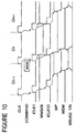
- Figure 10 is a timing chart illustrating an operation of the synchronous semiconductor memory shown in Figure 9.
- Figure 10 is a timing chart illustrating an operation of the synchronous semiconductor memory shown in Figure 9.
- Figure 10 is a timing chart illustrating an operation of the synchronous semiconductor memory shown in Figure 9.
- some part of the operation of the third embodiment is the same as that of the first embodiment, only a featured portion of the operation of the third embodiment will be described.
- the write mask control circuit 18 brings the write mask control signal WMSKB to a low (active) level in response to the internal synchronous signal ICLK1 which assumes the high level in response to the external clock CLK. Therefore, even if the internal synchronous signal ICLK1D is brought to the high level in the cycle Cn, the output of the NAND gate NAN2 is maintained at the high level.
- the write pulse is brought to the low level at once in response to the rising of the internal synchronous signal ICLK1D, the write pulse is maintained at the low level during the cycle Cn, so that the writing is not conducted in this cycle Cn. Namely, the writing is masked in this cycle Cn.
- the write mask control signal WMSKB is brought to a high (inactive) level in response to the internal synchronous signal ICLK1. Therefore, when the internal synchronous signal ICLK1D is brought to the high level, the output of the NAND gate NAN2 is brought to the low (not shown in Figure 10), and the write pulse WP is brought to the high level after the predetermined delay time.
- the synchronous semiconductor memory in accordance with the present invention is characterized in that the write execution time can be elongated dependently upon the cycle time t CK . Therefore, although the required write execution time t WP is different from one semiconductor memory to another because of a manufacturing process variation, the write execution time can be made to a minimum write execution time required when each memory device is operated with a minimum cycle time.
- the cycle time t CK can be shortened.
- a memory device requiring a long write execution time will never become a defective product, by lowering the speed grade and operating the memory device with a long cycle time t CK .
Landscapes
- Engineering & Computer Science (AREA)
- Microelectronics & Electronic Packaging (AREA)
- Computer Hardware Design (AREA)
- Dram (AREA)
- Static Random-Access Memory (AREA)
Applications Claiming Priority (3)
| Application Number | Priority Date | Filing Date | Title |
|---|---|---|---|
| JP29285495 | 1995-11-10 | ||
| JP7292854A JP2904076B2 (ja) | 1995-11-10 | 1995-11-10 | 半導体記憶装置 |
| JP292854/95 | 1995-11-10 |
Publications (3)
| Publication Number | Publication Date |
|---|---|
| EP0773549A2 true EP0773549A2 (de) | 1997-05-14 |
| EP0773549A3 EP0773549A3 (de) | 1998-12-02 |
| EP0773549B1 EP0773549B1 (de) | 2002-03-06 |
Family
ID=17787236
Family Applications (1)
| Application Number | Title | Priority Date | Filing Date |
|---|---|---|---|
| EP96118057A Expired - Lifetime EP0773549B1 (de) | 1995-11-10 | 1996-11-11 | Synchroner Halbleiterspeicher mit einem systemzyklusabhängigen Schreibausführungszyklus |
Country Status (6)
| Country | Link |
|---|---|
| US (1) | US5867447A (de) |
| EP (1) | EP0773549B1 (de) |
| JP (1) | JP2904076B2 (de) |
| KR (1) | KR100230115B1 (de) |
| DE (1) | DE69619620T2 (de) |
| TW (1) | TW486695B (de) |
Cited By (2)
| Publication number | Priority date | Publication date | Assignee | Title |
|---|---|---|---|---|
| FR2773233A1 (fr) * | 1997-11-18 | 1999-07-02 | Samsung Electronics Co Ltd | Circuit pour masquer des donnees et procede pour masquer des donnees d'un dispositif de memoire a semi-conducteurs |
| GB2345565A (en) * | 1998-12-24 | 2000-07-12 | Hyundai Electronics Ind | Internal command signal generator for synchronous memory |
Families Citing this family (19)
| Publication number | Priority date | Publication date | Assignee | Title |
|---|---|---|---|---|
| KR100277848B1 (ko) * | 1997-12-27 | 2001-01-15 | 김영환 | 반도체 메모리장치 |
| JPH11306758A (ja) * | 1998-04-27 | 1999-11-05 | Matsushita Electric Ind Co Ltd | 半導体記憶装置 |
| US6055208A (en) | 1998-06-05 | 2000-04-25 | Micron Technology, Inc. | Method and circuit for sending a signal in a semiconductor device during a setup time |
| JP2000048565A (ja) * | 1998-07-29 | 2000-02-18 | Mitsubishi Electric Corp | 同期型半導体記憶装置 |
| JP3076309B2 (ja) * | 1998-09-17 | 2000-08-14 | 日本電気アイシーマイコンシステム株式会社 | 半導体記憶装置 |
| JP4156721B2 (ja) * | 1998-09-18 | 2008-09-24 | 富士通株式会社 | 半導体集積回路装置 |
| JP3725715B2 (ja) * | 1998-11-27 | 2005-12-14 | 株式会社東芝 | クロック同期システム |
| JP3362775B2 (ja) * | 1998-12-25 | 2003-01-07 | インターナショナル・ビジネス・マシーンズ・コーポレーション | Dram及びdramのデータ・アクセス方法 |
| KR100304963B1 (ko) * | 1998-12-29 | 2001-09-24 | 김영환 | 반도체메모리 |
| KR100359157B1 (ko) * | 1998-12-30 | 2003-01-24 | 주식회사 하이닉스반도체 | 라이트 명령어 레이턴시회로 및 그 제어방법 |
| JP2000207900A (ja) * | 1999-01-12 | 2000-07-28 | Mitsubishi Electric Corp | 同期型半導体記憶装置 |
| KR100314807B1 (ko) * | 1999-12-28 | 2001-11-17 | 박종섭 | 반도체메모리 장치의 파이프 제어 장치 |
| US6621761B2 (en) * | 2000-05-31 | 2003-09-16 | Advanced Micro Devices, Inc. | Burst architecture for a flash memory |
| DE10115880B4 (de) * | 2001-03-30 | 2007-01-25 | Infineon Technologies Ag | Testschaltung zum kritischen Testen einer synchronen Speicherschaltung |
| KR100428684B1 (ko) * | 2001-09-24 | 2004-04-30 | 주식회사 하이닉스반도체 | 제어신호의 마스킹을 고려한 반도체 기억장치 |
| KR100519877B1 (ko) * | 2003-12-19 | 2005-10-10 | 삼성전자주식회사 | 레이트 라이트 기능을 갖는 반도체 메모리 장치 및 그데이터 입출력방법 |
| JP4005576B2 (ja) * | 2004-03-12 | 2007-11-07 | 松下電器産業株式会社 | 半導体集積回路装置 |
| JP2007184052A (ja) | 2006-01-10 | 2007-07-19 | Elpida Memory Inc | コマンド生成回路及びこれらを備えた半導体記憶装置 |
| KR102900753B1 (ko) * | 2021-09-10 | 2025-12-18 | 에스케이하이닉스 주식회사 | 데이터 출력 제어 회로 및 이를 포함하는 반도체 장치 |
Citations (2)
| Publication number | Priority date | Publication date | Assignee | Title |
|---|---|---|---|---|
| US5341341A (en) | 1992-03-26 | 1994-08-23 | Nec Corporation | Dynamic random access memory device having addressing section and/or data transferring path arranged in pipeline architecture |
| EP0704848A2 (de) | 1994-09-28 | 1996-04-03 | Nec Corporation | Fliessband-Halbleiterspeicheranordnung, die Zeitverlust beim Datenzugriff aufgrund des Unterschieds zwischen Fliessbandstufen eliminiert |
Family Cites Families (9)
| Publication number | Priority date | Publication date | Assignee | Title |
|---|---|---|---|---|
| US4476401A (en) * | 1983-01-31 | 1984-10-09 | Motorola, Inc. | Write strobe generator for clock synchronized memory |
| JPS61148692A (ja) * | 1984-12-24 | 1986-07-07 | Nippon Telegr & Teleph Corp <Ntt> | 記憶装置 |
| US4712190A (en) * | 1985-01-25 | 1987-12-08 | Digital Equipment Corporation | Self-timed random access memory chip |
| JP2536136B2 (ja) * | 1989-03-20 | 1996-09-18 | 日本電気株式会社 | 半導体記憶装置 |
| JP3179788B2 (ja) * | 1991-01-17 | 2001-06-25 | 三菱電機株式会社 | 半導体記憶装置 |
| JP3105318B2 (ja) * | 1991-12-19 | 2000-10-30 | 株式会社 沖マイクロデザイン | 半導体集積回路装置 |
| JP3591887B2 (ja) * | 1994-09-12 | 2004-11-24 | 富士通株式会社 | 半導体記憶装置 |
| JP2697634B2 (ja) * | 1994-09-30 | 1998-01-14 | 日本電気株式会社 | 同期型半導体記憶装置 |
| JP2692638B2 (ja) * | 1995-03-31 | 1997-12-17 | 日本電気株式会社 | 不揮発性半導体メモリ |
-
1995
- 1995-11-10 JP JP7292854A patent/JP2904076B2/ja not_active Expired - Fee Related
-
1996
- 1996-11-09 TW TW085113699A patent/TW486695B/zh not_active IP Right Cessation
- 1996-11-11 EP EP96118057A patent/EP0773549B1/de not_active Expired - Lifetime
- 1996-11-11 KR KR1019960053185A patent/KR100230115B1/ko not_active Expired - Fee Related
- 1996-11-11 DE DE69619620T patent/DE69619620T2/de not_active Expired - Lifetime
- 1996-11-12 US US08/745,821 patent/US5867447A/en not_active Expired - Lifetime
Patent Citations (2)
| Publication number | Priority date | Publication date | Assignee | Title |
|---|---|---|---|---|
| US5341341A (en) | 1992-03-26 | 1994-08-23 | Nec Corporation | Dynamic random access memory device having addressing section and/or data transferring path arranged in pipeline architecture |
| EP0704848A2 (de) | 1994-09-28 | 1996-04-03 | Nec Corporation | Fliessband-Halbleiterspeicheranordnung, die Zeitverlust beim Datenzugriff aufgrund des Unterschieds zwischen Fliessbandstufen eliminiert |
Cited By (6)
| Publication number | Priority date | Publication date | Assignee | Title |
|---|---|---|---|---|
| FR2773233A1 (fr) * | 1997-11-18 | 1999-07-02 | Samsung Electronics Co Ltd | Circuit pour masquer des donnees et procede pour masquer des donnees d'un dispositif de memoire a semi-conducteurs |
| DE19852986B4 (de) * | 1997-11-18 | 2011-02-03 | Samsung Electronics Co., Ltd., Suwon | Schaltungsanordnung und Verfahren zur Datenmaskierung |
| GB2345565A (en) * | 1998-12-24 | 2000-07-12 | Hyundai Electronics Ind | Internal command signal generator for synchronous memory |
| US6449674B1 (en) | 1998-12-24 | 2002-09-10 | Hyundai Electronics Industries Co., Ltd. | Internal command signal generator and method therefor |
| GB2345565B (en) * | 1998-12-24 | 2003-02-19 | Hyundai Electronics Ind | Internal command signal generator and method therefor |
| DE19962510B4 (de) * | 1998-12-24 | 2011-07-28 | Hyundai Electronics Industries Co., Ltd., Kyonggi | Vorrichtung zum Erzeugen eines internen Befehlsignals und Verfahren hierfür |
Also Published As
| Publication number | Publication date |
|---|---|
| EP0773549A3 (de) | 1998-12-02 |
| KR970029794A (ko) | 1997-06-26 |
| US5867447A (en) | 1999-02-02 |
| JPH09139084A (ja) | 1997-05-27 |
| DE69619620D1 (de) | 2002-04-11 |
| JP2904076B2 (ja) | 1999-06-14 |
| EP0773549B1 (de) | 2002-03-06 |
| TW486695B (en) | 2002-05-11 |
| KR100230115B1 (ko) | 1999-11-15 |
| DE69619620T2 (de) | 2002-11-07 |
Similar Documents
| Publication | Publication Date | Title |
|---|---|---|
| EP0773549B1 (de) | Synchroner Halbleiterspeicher mit einem systemzyklusabhängigen Schreibausführungszyklus | |
| US7327613B2 (en) | Input circuit for a memory device | |
| US5581512A (en) | Synchronized semiconductor memory | |
| KR100240539B1 (ko) | 입력 버퍼 회로의 소모 전류가 저감된 동기형 반도체 기억 장치 | |
| US7200069B2 (en) | Semiconductor memory device having external data load signal synchronous with data strobe signal and serial-to-parallel data prefetch method thereof | |
| US8276027B2 (en) | Semiconductor memory and method for testing the same | |
| US6636444B2 (en) | Semiconductor memory device having improved data transfer rate without providing a register for holding write data | |
| US6061292A (en) | Method and circuit for triggering column select line for write operations | |
| KR100414413B1 (ko) | 반도체 기억장치 | |
| US20040088475A1 (en) | Memory device with column select being variably delayed | |
| US6163500A (en) | Memory with combined synchronous burst and bus efficient functionality | |
| JP3180317B2 (ja) | 半導体記憶装置 | |
| US6636443B2 (en) | Semiconductor memory device having row buffers | |
| KR20070108293A (ko) | 반도체기억장치 | |
| US4602356A (en) | Semiconductor memory device | |
| KR100419270B1 (ko) | 반도체 메모리 | |
| US6166970A (en) | Priority determining apparatus using the least significant bit and CAS latency signal in DDR SDRAM device | |
| EP0766251A2 (de) | Halbleiterspeicheranordnung mit erweitertem Bereich eines verriegelbaren Eingangssignals | |
| KR19980018015A (ko) | 내부 동작 주파수 설정 가능한 dram | |
| EP1324341B1 (de) | Verfahren zum Datenzugriff in einer Auffrischung benötigenden Halbleiterspeicheranordnung und Halbleiterspeicheranordnung dafür | |
| KR100324143B1 (ko) | 반도체 메모리장치 및 번인 테스트 방법 | |
| US8050135B2 (en) | Semiconductor memory device | |
| KR100650845B1 (ko) | 소비 전력을 감소시키는 버퍼 제어 회로와, 이를 포함하는메모리 모듈용 반도체 메모리 장치 및 그 제어 동작 방법 | |
| US6504767B1 (en) | Double data rate memory device having output data path with different number of latches | |
| KR100275722B1 (ko) | 동기식 랜덤 엑세스 메모리 제어 장치 및 방법 |
Legal Events
| Date | Code | Title | Description |
|---|---|---|---|
| PUAI | Public reference made under article 153(3) epc to a published international application that has entered the european phase |
Free format text: ORIGINAL CODE: 0009012 |
|
| AK | Designated contracting states |
Kind code of ref document: A2 Designated state(s): DE FR GB |
|
| PUAL | Search report despatched |
Free format text: ORIGINAL CODE: 0009013 |
|
| AK | Designated contracting states |
Kind code of ref document: A3 Designated state(s): DE FR GB |
|
| 17P | Request for examination filed |
Effective date: 19990301 |
|
| 17Q | First examination report despatched |
Effective date: 20000503 |
|
| GRAG | Despatch of communication of intention to grant |
Free format text: ORIGINAL CODE: EPIDOS AGRA |
|
| GRAG | Despatch of communication of intention to grant |
Free format text: ORIGINAL CODE: EPIDOS AGRA |
|
| GRAH | Despatch of communication of intention to grant a patent |
Free format text: ORIGINAL CODE: EPIDOS IGRA |
|
| GRAH | Despatch of communication of intention to grant a patent |
Free format text: ORIGINAL CODE: EPIDOS IGRA |
|
| REG | Reference to a national code |
Ref country code: GB Ref legal event code: IF02 |
|
| GRAA | (expected) grant |
Free format text: ORIGINAL CODE: 0009210 |
|
| AK | Designated contracting states |
Kind code of ref document: B1 Designated state(s): DE FR GB |
|
| REF | Corresponds to: |
Ref document number: 69619620 Country of ref document: DE Date of ref document: 20020411 |
|
| ET | Fr: translation filed | ||
| PLBE | No opposition filed within time limit |
Free format text: ORIGINAL CODE: 0009261 |
|
| STAA | Information on the status of an ep patent application or granted ep patent |
Free format text: STATUS: NO OPPOSITION FILED WITHIN TIME LIMIT |
|
| 26N | No opposition filed |
Effective date: 20021209 |
|
| REG | Reference to a national code |
Ref country code: GB Ref legal event code: 732E |
|
| REG | Reference to a national code |
Ref country code: GB Ref legal event code: 732E |
|
| REG | Reference to a national code |
Ref country code: FR Ref legal event code: TQ |
|
| REG | Reference to a national code |
Ref country code: GB Ref legal event code: 732E |
|
| REG | Reference to a national code |
Ref country code: FR Ref legal event code: TP |
|
| REG | Reference to a national code |
Ref country code: FR Ref legal event code: CD |
|
| REG | Reference to a national code |
Ref country code: DE Ref legal event code: R082 Ref document number: 69619620 Country of ref document: DE Representative=s name: BETTEN & RESCH, DE |
|
| REG | Reference to a national code |
Ref country code: DE Ref legal event code: R082 Ref document number: 69619620 Country of ref document: DE Representative=s name: BETTEN & RESCH PATENT- UND RECHTSANWAELTE PART, DE Effective date: 20120828 Ref country code: DE Ref legal event code: R082 Ref document number: 69619620 Country of ref document: DE Representative=s name: PATENTANWAELTE BETTEN & RESCH, DE Effective date: 20120828 Ref country code: DE Ref legal event code: R081 Ref document number: 69619620 Country of ref document: DE Owner name: RENESAS ELECTRONICS CORPORATION, KAWASAKI-SHI, JP Free format text: FORMER OWNER: NEC ELECTRONICS CORP., KAWASAKI, KANAGAWA, JP Effective date: 20120828 Ref country code: DE Ref legal event code: R081 Ref document number: 69619620 Country of ref document: DE Owner name: RENESAS ELECTRONICS CORPORATION, JP Free format text: FORMER OWNER: NEC ELECTRONICS CORP., KAWASAKI, JP Effective date: 20120828 |
|
| PGFP | Annual fee paid to national office [announced via postgrant information from national office to epo] |
Ref country code: FR Payment date: 20121130 Year of fee payment: 17 Ref country code: DE Payment date: 20121107 Year of fee payment: 17 |
|
| PGFP | Annual fee paid to national office [announced via postgrant information from national office to epo] |
Ref country code: GB Payment date: 20121107 Year of fee payment: 17 |
|
| GBPC | Gb: european patent ceased through non-payment of renewal fee |
Effective date: 20131111 |
|
| REG | Reference to a national code |
Ref country code: FR Ref legal event code: ST Effective date: 20140731 |
|
| PG25 | Lapsed in a contracting state [announced via postgrant information from national office to epo] |
Ref country code: DE Free format text: LAPSE BECAUSE OF NON-PAYMENT OF DUE FEES Effective date: 20140603 |
|
| REG | Reference to a national code |
Ref country code: DE Ref legal event code: R119 Ref document number: 69619620 Country of ref document: DE Effective date: 20140603 |
|
| PG25 | Lapsed in a contracting state [announced via postgrant information from national office to epo] |
Ref country code: FR Free format text: LAPSE BECAUSE OF NON-PAYMENT OF DUE FEES Effective date: 20131202 Ref country code: GB Free format text: LAPSE BECAUSE OF NON-PAYMENT OF DUE FEES Effective date: 20131111 |