EP0773574A1 - Feldemissionsvorrichtungen mit Emittern auf Metallfolie und Verfahren zur Herstellung dieser Vorrichtungen - Google Patents
Feldemissionsvorrichtungen mit Emittern auf Metallfolie und Verfahren zur Herstellung dieser Vorrichtungen Download PDFInfo
- Publication number
- EP0773574A1 EP0773574A1 EP96307791A EP96307791A EP0773574A1 EP 0773574 A1 EP0773574 A1 EP 0773574A1 EP 96307791 A EP96307791 A EP 96307791A EP 96307791 A EP96307791 A EP 96307791A EP 0773574 A1 EP0773574 A1 EP 0773574A1
- Authority
- EP
- European Patent Office
- Prior art keywords
- metal foil
- diamond
- sheet
- foil
- field emission
- Prior art date
- Legal status (The legal status is an assumption and is not a legal conclusion. Google has not performed a legal analysis and makes no representation as to the accuracy of the status listed.)
- Granted
Links
- 239000011888 foil Substances 0.000 title claims abstract description 88
- 229910052751 metal Inorganic materials 0.000 title claims abstract description 75
- 239000002184 metal Substances 0.000 title claims abstract description 75
- 238000000034 method Methods 0.000 title claims abstract description 29
- 229910003460 diamond Inorganic materials 0.000 claims abstract description 69
- 239000010432 diamond Substances 0.000 claims abstract description 69
- 239000002245 particle Substances 0.000 claims abstract description 40
- 239000000758 substrate Substances 0.000 claims abstract description 32
- 239000011521 glass Substances 0.000 claims abstract description 20
- 239000000463 material Substances 0.000 claims description 34
- 239000001257 hydrogen Substances 0.000 claims description 22
- 229910052739 hydrogen Inorganic materials 0.000 claims description 22
- UFHFLCQGNIYNRP-UHFFFAOYSA-N Hydrogen Chemical compound [H][H] UFHFLCQGNIYNRP-UHFFFAOYSA-N 0.000 claims description 20
- 238000000151 deposition Methods 0.000 claims description 14
- 239000011248 coating agent Substances 0.000 claims description 13
- 238000000576 coating method Methods 0.000 claims description 13
- 230000008021 deposition Effects 0.000 claims description 12
- 229910052710 silicon Inorganic materials 0.000 claims description 9
- 239000007921 spray Substances 0.000 claims description 7
- 239000000203 mixture Substances 0.000 claims description 6
- 238000001035 drying Methods 0.000 claims description 5
- 238000000059 patterning Methods 0.000 claims description 5
- 229910052750 molybdenum Inorganic materials 0.000 claims description 4
- 230000001464 adherent effect Effects 0.000 claims description 3
- 229910052735 hafnium Inorganic materials 0.000 claims description 3
- 229910052719 titanium Inorganic materials 0.000 claims description 3
- 229910052721 tungsten Inorganic materials 0.000 claims description 3
- 229910052720 vanadium Inorganic materials 0.000 claims description 3
- 229910052726 zirconium Inorganic materials 0.000 claims description 3
- 229910002704 AlGaN Inorganic materials 0.000 claims description 2
- 239000004020 conductor Substances 0.000 abstract description 17
- 238000010438 heat treatment Methods 0.000 abstract description 17
- 230000008569 process Effects 0.000 abstract description 7
- 238000004519 manufacturing process Methods 0.000 abstract description 5
- 238000005229 chemical vapour deposition Methods 0.000 description 19
- 238000009832 plasma treatment Methods 0.000 description 8
- VNWKTOKETHGBQD-UHFFFAOYSA-N methane Chemical compound C VNWKTOKETHGBQD-UHFFFAOYSA-N 0.000 description 6
- 239000000126 substance Substances 0.000 description 6
- OAICVXFJPJFONN-UHFFFAOYSA-N Phosphorus Chemical compound [P] OAICVXFJPJFONN-UHFFFAOYSA-N 0.000 description 5
- XUIMIQQOPSSXEZ-UHFFFAOYSA-N Silicon Chemical compound [Si] XUIMIQQOPSSXEZ-UHFFFAOYSA-N 0.000 description 5
- 238000010586 diagram Methods 0.000 description 5
- 239000007789 gas Substances 0.000 description 5
- 229910000833 kovar Inorganic materials 0.000 description 5
- 238000002844 melting Methods 0.000 description 5
- 230000008018 melting Effects 0.000 description 5
- 239000010703 silicon Substances 0.000 description 5
- 238000005507 spraying Methods 0.000 description 5
- 229910045601 alloy Inorganic materials 0.000 description 4
- 239000000956 alloy Substances 0.000 description 4
- 238000001704 evaporation Methods 0.000 description 4
- 230000008020 evaporation Effects 0.000 description 4
- 239000007788 liquid Substances 0.000 description 4
- 230000004913 activation Effects 0.000 description 3
- 239000011230 binding agent Substances 0.000 description 3
- 238000010924 continuous production Methods 0.000 description 3
- 239000010408 film Substances 0.000 description 3
- 238000010849 ion bombardment Methods 0.000 description 3
- 239000011159 matrix material Substances 0.000 description 3
- 239000000843 powder Substances 0.000 description 3
- 238000005086 pumping Methods 0.000 description 3
- CSCPPACGZOOCGX-UHFFFAOYSA-N Acetone Chemical compound CC(C)=O CSCPPACGZOOCGX-UHFFFAOYSA-N 0.000 description 2
- XKRFYHLGVUSROY-UHFFFAOYSA-N Argon Chemical compound [Ar] XKRFYHLGVUSROY-UHFFFAOYSA-N 0.000 description 2
- 239000004215 Carbon black (E152) Substances 0.000 description 2
- YZCKVEUIGOORGS-UHFFFAOYSA-N Hydrogen atom Chemical compound [H] YZCKVEUIGOORGS-UHFFFAOYSA-N 0.000 description 2
- 230000008901 benefit Effects 0.000 description 2
- 239000010406 cathode material Substances 0.000 description 2
- 238000009792 diffusion process Methods 0.000 description 2
- 230000005684 electric field Effects 0.000 description 2
- 238000000609 electron-beam lithography Methods 0.000 description 2
- 238000011049 filling Methods 0.000 description 2
- 238000009501 film coating Methods 0.000 description 2
- 229930195733 hydrocarbon Natural products 0.000 description 2
- 150000002430 hydrocarbons Chemical class 0.000 description 2
- 150000002431 hydrogen Chemical class 0.000 description 2
- 238000011065 in-situ storage Methods 0.000 description 2
- 150000002739 metals Chemical class 0.000 description 2
- 239000002113 nanodiamond Substances 0.000 description 2
- 230000006911 nucleation Effects 0.000 description 2
- 238000010899 nucleation Methods 0.000 description 2
- 230000005855 radiation Effects 0.000 description 2
- 238000007789 sealing Methods 0.000 description 2
- 239000004065 semiconductor Substances 0.000 description 2
- 229910000679 solder Inorganic materials 0.000 description 2
- 238000004544 sputter deposition Methods 0.000 description 2
- 239000010409 thin film Substances 0.000 description 2
- 229910052718 tin Inorganic materials 0.000 description 2
- QGZKDVFQNNGYKY-UHFFFAOYSA-N Ammonia Chemical compound N QGZKDVFQNNGYKY-UHFFFAOYSA-N 0.000 description 1
- 229910016338 Bi—Sn Inorganic materials 0.000 description 1
- 229910020711 Co—Si Inorganic materials 0.000 description 1
- 229910017758 Cu-Si Inorganic materials 0.000 description 1
- 229910017931 Cu—Si Inorganic materials 0.000 description 1
- LFQSCWFLJHTTHZ-UHFFFAOYSA-N Ethanol Chemical compound CCO LFQSCWFLJHTTHZ-UHFFFAOYSA-N 0.000 description 1
- 229910017082 Fe-Si Inorganic materials 0.000 description 1
- 229910017133 Fe—Si Inorganic materials 0.000 description 1
- 229910017305 Mo—Si Inorganic materials 0.000 description 1
- 229910018098 Ni-Si Inorganic materials 0.000 description 1
- 229910018529 Ni—Si Inorganic materials 0.000 description 1
- 229910020220 Pb—Sn Inorganic materials 0.000 description 1
- 239000004642 Polyimide Substances 0.000 description 1
- 229910004339 Ti-Si Inorganic materials 0.000 description 1
- 229910010978 Ti—Si Inorganic materials 0.000 description 1
- 229910007735 Zr—Si Inorganic materials 0.000 description 1
- 239000000853 adhesive Substances 0.000 description 1
- 230000001070 adhesive effect Effects 0.000 description 1
- 238000005275 alloying Methods 0.000 description 1
- 229910052782 aluminium Inorganic materials 0.000 description 1
- XAGFODPZIPBFFR-UHFFFAOYSA-N aluminium Chemical compound [Al] XAGFODPZIPBFFR-UHFFFAOYSA-N 0.000 description 1
- 230000003466 anti-cipated effect Effects 0.000 description 1
- 229910052786 argon Inorganic materials 0.000 description 1
- 230000009286 beneficial effect Effects 0.000 description 1
- 239000000919 ceramic Substances 0.000 description 1
- 238000006243 chemical reaction Methods 0.000 description 1
- 229910052802 copper Inorganic materials 0.000 description 1
- 230000007547 defect Effects 0.000 description 1
- 238000001652 electrophoretic deposition Methods 0.000 description 1
- 238000005516 engineering process Methods 0.000 description 1
- 238000005530 etching Methods 0.000 description 1
- 238000002474 experimental method Methods 0.000 description 1
- 239000003574 free electron Substances 0.000 description 1
- 238000004050 hot filament vapor deposition Methods 0.000 description 1
- 229910052738 indium Inorganic materials 0.000 description 1
- AMGQUBHHOARCQH-UHFFFAOYSA-N indium;oxotin Chemical compound [In].[Sn]=O AMGQUBHHOARCQH-UHFFFAOYSA-N 0.000 description 1
- 238000000608 laser ablation Methods 0.000 description 1
- 239000011344 liquid material Substances 0.000 description 1
- 238000012986 modification Methods 0.000 description 1
- 230000004048 modification Effects 0.000 description 1
- 229910052759 nickel Inorganic materials 0.000 description 1
- 150000004767 nitrides Chemical class 0.000 description 1
- 238000010943 off-gassing Methods 0.000 description 1
- 238000005192 partition Methods 0.000 description 1
- 230000002093 peripheral effect Effects 0.000 description 1
- 238000000206 photolithography Methods 0.000 description 1
- 229920001721 polyimide Polymers 0.000 description 1
- 239000012254 powdered material Substances 0.000 description 1
- 238000002360 preparation method Methods 0.000 description 1
- 238000003825 pressing Methods 0.000 description 1
- 230000001737 promoting effect Effects 0.000 description 1
- 238000007761 roller coating Methods 0.000 description 1
- 238000005245 sintering Methods 0.000 description 1
- 239000007787 solid Substances 0.000 description 1
- 238000007711 solidification Methods 0.000 description 1
- 230000008023 solidification Effects 0.000 description 1
- 239000002904 solvent Substances 0.000 description 1
- 238000002207 thermal evaporation Methods 0.000 description 1
- 238000007736 thin film deposition technique Methods 0.000 description 1
- 230000001052 transient effect Effects 0.000 description 1
- XCZXGTMEAKBVPV-UHFFFAOYSA-N trimethylgallium Chemical compound C[Ga](C)C XCZXGTMEAKBVPV-UHFFFAOYSA-N 0.000 description 1
- 239000011882 ultra-fine particle Substances 0.000 description 1
- XLYOFNOQVPJJNP-UHFFFAOYSA-N water Substances O XLYOFNOQVPJJNP-UHFFFAOYSA-N 0.000 description 1
- 238000004804 winding Methods 0.000 description 1
Images


Classifications
-
- H—ELECTRICITY
- H01—ELECTRIC ELEMENTS
- H01J—ELECTRIC DISCHARGE TUBES OR DISCHARGE LAMPS
- H01J9/00—Apparatus or processes specially adapted for the manufacture, installation, removal, maintenance of electric discharge tubes, discharge lamps, or parts thereof; Recovery of material from discharge tubes or lamps
- H01J9/02—Manufacture of electrodes or electrode systems
- H01J9/022—Manufacture of electrodes or electrode systems of cold cathodes
- H01J9/025—Manufacture of electrodes or electrode systems of cold cathodes of field emission cathodes
-
- H—ELECTRICITY
- H01—ELECTRIC ELEMENTS
- H01J—ELECTRIC DISCHARGE TUBES OR DISCHARGE LAMPS
- H01J2201/00—Electrodes common to discharge tubes
- H01J2201/30—Cold cathodes
- H01J2201/304—Field emission cathodes
- H01J2201/30403—Field emission cathodes characterised by the emitter shape
-
- H—ELECTRICITY
- H01—ELECTRIC ELEMENTS
- H01J—ELECTRIC DISCHARGE TUBES OR DISCHARGE LAMPS
- H01J2201/00—Electrodes common to discharge tubes
- H01J2201/30—Cold cathodes
- H01J2201/304—Field emission cathodes
- H01J2201/30446—Field emission cathodes characterised by the emitter material
- H01J2201/30453—Carbon types
- H01J2201/30457—Diamond
Definitions
- This invention pertains to field emission devices and, in particular, to field emission devices, such as flat panel displays, using improved electron emitter particles or islands pre-deposited and adhered on metal foil, and the methods for making such devices.
- Field emission of electrons into vacuum from suitable cathode materials is currently the most promising source of electrons for a variety of vacuum devices. These devices include flat panel displays, klystrons and traveling wave tubes used in microwave power amplifiers, ion guns, electron beam lithography, high energy accelerators, free electron lasers, and electron microscopes and microprobes. A most promising application is the use of field emitters in thin, matrix-addressed flat panel displays. See, for example, the December 1991 issue of Semiconductor International, p. 46; C. A. Spindt et al., IEEE Transactions on Electron Devices, vol. 38, p. 2355 (1991); I. Brodie and C. A.
- a typical field emission device comprises a cathode including a plurality of field emitter tips and an anode spaced from the cathode.
- a voltage applied between the anode and cathode induces the emission of electrons towards the anode.
- a conventional flat panel field emission display comprises a flat vacuum cell having a matrix array of microscopic field emitters formed on a cathode of the cell (the back plate) and a phosphor coated anode on a transparent front plate. Between cathode and anode is a conductive element called a grid or gate. The cathodes and gates are typically skewed strips (usually perpendicular) whose crossovers define pixels for the display. A given pixel is activated by applying voltage between the cathode conductor strip and the gate conductor. A more positive voltage is applied to the anode in order to impart a relatively high energy (400-3,000 eV) to the emitted electrons. See for example, United States Patents Nos. 4,940,916; 5,129,850; 5,138,237 and 5,283,500, each of which is incorporated herein by reference.
- the cathode materials useful for field emission devices should have the following characteristics:
- Previous electron emitters were typically made of metal (such as Mo) or semiconductor (such as Si) with sharp tips in nanometer sizes. Reasonable emission characteristics with stability and reproducibility necessary for practical applications have been demonstrated.
- the control voltage required for emission from these materials is relatively high (around 100 V) because of their high work functions.
- the high voltage operation increases the damaging instabilities due to ion bombardment and surface diffusion on the emitter tips and necessitates high power densities from an external source.
- the fabrication of uniform sharp tips is difficult, tedious and expensive, especially over a large area.
- the vulnerability of these materials to ion bombardment, chemically active species and temperature extremes is a serious concern.
- Diamond is a desirable material for field emitters because of its negative or low electron affinity and robust mechanical and chemical properties.
- Field emission devices employing diamond field emitters are disclosed, for example, in United States Patents Nos. 5,129,850 and 5,138,237 and in Okano et al., Appl. Phys. Lett ., vol. 64, p. 2742 (1994), all of which are incorporated herein by reference.
- Flat panel displays which can employ diamond emitters are disclosed in co-pending United States Patent application Serial No. 08/220,077 filed by Eom et al on March 30, 1994, United States Patent applications Serial No. 08/299,674 and Serial No. 08/299,470, both filed by Jin et al. on August 31, 1994, and United States Patent application Serial No. 08/311,458 and No. 08/332,179, both filed by Jin et al. on October 31, 1994, Serial No. 08/361616 filed on December 22, 1994, and Serial No. 08/381375 filed on January 31, 1995.
- Diamond offers substantial advantages as low-voltage field emitters, especially diamond in the form of ultra fine particles or islands. These particles or islands can be made to exhibit sharp, protruding crystallographic edges and corners desirable for the concentration of an electric field.
- One of the most critical preparation steps for ensuring low-voltage field emission is the chemical bonding of the diamond particles or islands onto the surface of cathode conductor for good electrical contact. Experimental results teach that without strong bonding and associated good electrical contact, low-voltage field emission from diamond is not possible.
- ultra fine or nanometer-type diamond particles such as those disclosed in Application Serial No. 08/361616 and Serial No. 08/381375
- a good adhesion of the particles to the conductive substrate can be achieved by high-temperature heat treatment of the particles on the substrate in hydrogen plasma, typically at 300-1000° C. While adequate emission characteristics can be obtained by the plasma heat treatment even below about 500° C, further improved properties are generally achieved by higher temperature processing.
- the glass substrate desirably has a low melting point of about 550° C or below for the purpose of ease of vacuum sealing when the FED assembly is completed. This places an undue upper limit in the plasma heat treatment temperature and hence restricts the full utilization of the best attainable field emission characteristics from the diamond particles.
- the present invention provides improved methods for making field emission devices by which one can pre-deposit and bond the diamond particles or islands on a flexible metal foil at a desirably high temperature (e.g., near 900° C or higher), and then subsequently attach the high-quality- emitter-coated conductor foil onto the glass substrate.
- a desirably high temperature e.g., near 900° C or higher
- these methods provide high-speed, low-cost manufacturing. Since the field emitters can be pre-deposited on the metal foil in the form of long continuous sheet wound as a roll, the cathode assembly can be made by a high-speed, automated bonding process without having to subject each of the emitter-coated glass substrates to plasma heat treatment in a vacuum chamber.
- FIG. 1 illustrates the steps of a preferred process for preparing an enhanced field emitter structure.
- the first step shown in Block A of FIG. 1 is to provide a flexible metal foil onto which field emitter material is to be deposited.
- carbide-forming metals such as Mo,W, Hf, Zr, Ti, V or Si be used, at least on the surface of the foil.
- the desirable thickness of the metal foil is typically in the range of 0.01-0.50 mm, preferably 0.02-0.10 mm.
- the advantage of the greater thickness of the foil as compared with conventional thin film coatings is that foil can conduct a higher electrical current with minimal heating.
- Silicon is particularly desirable for good diamond adhesion in the case of plasma heat treatment of spray-coated diamond particles and for good diamond nucleation in the case of CVD deposited diamond islands.
- silicon is brittle and is not readily available in flexible sheet form.
- silicon can be utilized in the form of thin, deposited layer on the surface of other flexible metal foils such as Ni, Co, Cu or Mo.
- Various thin film deposition methods such as sputtering, thermal deposition, e-beam evaporation, or chemical vapor deposition may be used to deposit a silicon film.
- the preferred thickness of a silicon coating is in the range 0.1-2 micron.
- Si can be incorporated into another flexible metal as an alloying element, to form alloys such as, Ni-Si, Fe-Si, Cu-Si, Co-Si, Mo-Si, Ti-Si or Zr-Si.
- alloys such as, Ni-Si, Fe-Si, Cu-Si, Co-Si, Mo-Si, Ti-Si or Zr-Si.
- the amount of Si in these alloys should be at least 2 and preferably at least 5 weight percent.
- the next step shown in block B of FIG. 1 is to pattern the flexible metal foil.
- the foil desirably wound on or unwound from a mandrel for high-speed processing, is advantageously patterned into a parallel stripe configuration with each stripe having the width of each cathode conductor.
- the patterning should maintain the structural integrity of the sheet so that it can be handled as a sheet even after metal is removed.
- FIG. 2 A typical pattern for use in making a plurality of display devices is shown in FIG. 2.
- the foil 20 is patterned by a plurality of etched away regions 21 into stripes 22.
- the overall size of each patterned region 21 can be slightly larger than the anticipated display substrate area 23 (shown in dashed lines).
- the orientation of the stripes can be either longitudinal or transverse but a longitudinal arrangement is preferred so that tension can be applied along the foil length during handling or processing to maintain the flatness of the foil.
- Such a stripe pattern can be obtained by a number of known patterning techniques such as photolithographic etching, laser cut-out (or local burn-off), or for coarse patterns, mechanical cut-out (e.g. by stamping operations).
- Typical flat panel displays have the conductor stripe width of about 100 ⁇ m. Together with the orthogonally placed gate stripes of the same width, for example, a 100 x 100 ⁇ m pixel size for field emission display is defined.
- the desirable stripe width is in the range of 10-500 ⁇ m, preferably 20-100 ⁇ m.
- the next step in the exemplary processing of FIG. 1 is to adhere field emitting material to the patterned foil.
- the preferred field emitters are ultra fine or nanometer diamond particles such as manufactured or sold by Dubble-Dee Harris as diamond grit or by E. I. DuPont under the product name Mypolex.
- the diamond particle size is predominantly in the range of 0.002-1 ⁇ m, and preferably 0.005-0.5 ⁇ m. Such small sizes are important for lowering of the electron affinity and enabling a low-voltage field emission of electrons.
- the diamond particles can be applied onto the metal foil by any known technique such as by spray coating a mixture of the particles and a volatile liquid medium (such as acetone, alcohol, water), by electrophoretic deposition, or by controlled sprinkling through fine sieves.
- a volatile liquid medium such as acetone, alcohol, water
- the coating typically applied in a thin layer about 0.01-10 ⁇ m thick.
- the layer typically is about 0.3-5.0 particles thick on average, and preferably 0.5-3 particles thick on average.
- a gentle heating to 50-100° C may be given to accelerate the drying of spray-coated powder through faster evaporation of the associated liquid medium.
- a small amount of organic binder such as used in typical ceramic powder sintering processing may be added to the liquid medium for improved adhesion of the particles.
- the binder material decomposes or volatilizes during the subsequent high temperature processing.
- non-particulate diamond field emitters can also be used.
- field emitters can be grown and adhered by chemical vapor deposition (CVD) of diamond islands (using 1-10 volume % methane in hydrogen at a temperature of 400-1100° C) on a flexible metal foil which is continuously or semi-continuously fed into the deposition chamber.
- CVD chemical vapor deposition
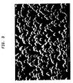
- An exemplary configuration of the islands is shown in FIG. 3. They were grown on a Si surface by microwave CVD deposition at ⁇ 900° C using a mixture of 2% methane in hydrogen.
- Other known deposition techniques such as DC plasma, RF plasma, hot filament, or hydrocarbon gas torch method can also be used.
- the flat-bottomed island geometry which is achieved in-situ during the CVD deposition is particularly beneficial.
- the islands tend to possess sharp crystallographic facets and corners pointing toward the anode for concentration of electric field for easier electron emission, and they ensure, unlike a continuous diamond film, short paths of electron transport from the underlying or nearby metal foil to the electron emitting tips.
- the desired size of the CVD deposited island is typically in the diameter range of 0.05-10 ⁇ m, and preferably 0.05-2 ⁇ m.
- the CVD deposition conditions can be adjusted so as to introduce more defects in the diamond islands (or at least on their surface), for example, as disclosed in application Serial No. 08/331458 filed September 22, 1995.
- metal foil instead of diamond, other low-voltage electron field emitters such as AIN or AIGaN can be deposited on the metal foil, either in the form of pre-made particles or as in-situ deposited islands. These materials are preferably deposited by CVD processing using thimethyl aluminum or trimethyl gallium in ammonia gas at 500-1100 ° C.
- the metal foil is preferably chosen from nitride-forming elements such as Mo, W, Hf, Zr, Ti, V, and Si.. Alternatively, these nitride forming metals can be deposited on another flexible metal as a thin film coating.
- the next step (Step D of FIG. 1) is to provide high temperature, hydrogen plasma heat treatment in order to ensure diffusion-induced chemical bonding between the applied ultra fine diamond particles and the metal foil substrate and also to induce hydrogen termination on diamond surface.
- the chemical bonding is important not only for good electrical contact for ease of electron transport from the metal foil to the tip of diamond emitters but also to provide mechanical stability of bonded diamond particles during various subsequent processing such as winding into rolls, unwinding from a mandrel for continuous feeding for high-speed display assembly, and possibly pressing/rubbing operation during the bonding of the metal foil onto the glass substrate.
- Typical hydrogen plasma heat treatment according to the invention is carried out at 400-1100° C, preferably 600-1000° C, even more preferably 800-1000° C.
- the optimal duration of plasma treatment can easily be determined by experiments but typically in the range of 1-1000 minutes, preferably 1-100 minutes.
- the hydrogen plasma or atomic hydrogen is generated by known methods such as microwave activation or hot filament activation.
- the plasma may contain less than 100% hydrogen, e.g., it may be mixture of hydrogen and argon.
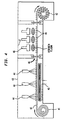
- FIG. 4 is a schematic cross-section of apparatus useful in processing foil with diamond emitters.
- the foil 40 is passed from an output mandrel 41 to takeup mandrel 42, passing through a coating chamber 43 where it is exposed to one or more nozzles 44 for spray-coating diamond particles.
- chamber 43 is provided with a heater 45 to facilitate drying of the spray coated particles.
- the coated foil After moving through chamber 43, as through a chamber partition door 46, the coated foil passes through a plasma treatment chamber 47 where the coated surface is subjected to hydrogen plasma created by one or more plasma generators 48.
- diamond particles 49 such as nanodiamond particles, are spray coated on the flexible metal, the liquid medium in the sprayed layer is then dried off, and the deposited diamond particles are then subjected to a hydrogen plasma heat treatment inside chamber 47.
- the procedure can be semi-continuous or continuous processing. However, for the ease of hydrogen plasma treatment which is typically carried out at a low gas pressure of about 0.1 atmosphere maintained in a closed chamber, semi-continuous plasma processing is more suitable for the particular sequence shown in FIG. 4. A bath type processing instead of semi-continuous or continuous processing is not excluded.
- the diamond particles are spray coated on newly arrived foil surface and dried immediately followed by vacuum pumping and back-filling with hydrogen partial pressure so as to be ready to be fed into the chamber.
- the operating cycle for each stationary step can take typically about 1-60 minutes, preferably about 2-10 minutes.
- 6 minutes can be spent on spraying and drying while the remaining 4 minutes are used for pumping and hydrogen back filling.
- plasma heat treatment continues in chamber 47.
- chamber 47 can be a differentially pumped plasma treatment system with two to ten steps of pumping (not shown) on each side of the plasma treatment center.
- the finished metal foil with the diamond emitter particles attached on its surface is wound on a mandrel for subsequent assembly into display devices.
- FIG. 5 illustrates alternative processing apparatus suitable for continuous processing.
- the apparatus is similar to that of FIG. 4 and the corresponding components are given the same reference numerals.
- the metal foil 40 is unwound from the left roll 41, diamond particles are continuously spray coated and dried.
- the metal foil continuously moves to the right, entering a transient chamber 50 which is bounded by two movable accordian-like shutters 51, 52 before entering the plasma treatment chamber 50.
- the shutter 51 to the left can grab onto the moving metal foil and travel with it to the right. After traveling a sufficient distance, the shutter releases the foil and moves back to the far left position and grabs a new site on the moving metal foil.
- the right shutter (not shown) closes on the foil during the short period when the left shutter releases and moves left to grab on a new site.
- a similar two-shutter system operates on the exit side of the plasma chamber so that the plasma heat treated metal foils can come out and wound on a mandrel without disturbing the low pressure hydrogen atmosphere (near 0.1 atmosphere
- an alternative processing uses atomic hydrogen at high temperature generated for example by hot filament heating. This treatment activates the diamond particle surface into hydrogen-terminated surface and to induce chemical bonding between the diamond particles and the metal foil substrate.
- CVD deposition of diamond island emitters such as depicted in FIG. 3 can be carried out by a batch processing, or preferably by semi-continuous or continuous processing.
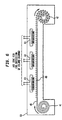
- FIG. 6 schematically illustrates exemplary apparatus for coating metal foil 40 with diamond island emitters.
- the foil is disposed in a CVD chamber 60 and passed near one or more hot filament heating elements 61 in the presence of an appropriate mixture of gases.
- Various other elements such as microwave plasma, RF or DC plasma, or a torch can be utilized in place of the hot filaments 61.
- Hot filament CVD deposition is in general cheaper in capital costs, and hence is preferred.
- the metal foil substrate can be mechanically abraded to promote diamond nucleation.
- the metal foil is continuously fed from left to right in the CVD chamber 60, going past the heating elements 61 where island diamond emitters are deposited and bonded onto the metal foil surface.
- Typical deposition conditions are; 0.5-6 vol. % methane (or various hydrocarbon gases) in hydrogen, 600-1000 ° C for 1-100 minute.
- the diamond islands are typically less than 2 ⁇ m in size.
- Step E is to adhere the emitter-coated metal foil onto an insulating substrate such as a glass substrate to form an array of cathode conductor lines.
- This step is illustrated schematically in FIG. 7 where metal foil 70 is being attached to glass substrate 71.
- the metal foil can additionally comprise on its backside a thin coating of adhesion-promoting material 72 which bonds the metal foil to the glass plate.
- the adhesion-promoting material can be a glass layer (e.g., low melting point glass with a melting point near 500° C), solder coating (e.g., In, In-Sn, Sn, Pb-Sn, Bi-Sn), glass-sealable alloy coating (e.g., the well-known, thermal-expansion-matching Kovar alloy, Fe-28% Ni-18% Co by weight), or a polymeric adhesive such as polyimide with minimal outgassing problems.
- solder coating e.g., In, In-Sn, Sn, Pb-Sn, Bi-Sn
- glass-sealable alloy coating e.g., the well-known, thermal-expansion-matching Kovar alloy, Fe-28% Ni-18% Co by weight
- a polymeric adhesive such as polyimide with minimal outgassing problems.
- These adhesion-promoting materials can be a solid layer, powdered material (with an optional binder and/or solvent mixed with it), or a liquid
- the adhesion-promoting material can be added on the backside of the metal foil either before the plasma heat treatment for the diamond particles (or the CVD processing for diamond islands) or after the treatment.
- Low-melting-point materials such as the solder or glass are preferably applied after the plasma treatment. Roller coating, brush coating, or line-of-sight spray coating or evaporation can be used for application of these materials.
- High-melting-point materials such as Kovar can be deposited before plasma treatment, using sputtering or e-beam evaporation.
- the metal foil itself can be made of Kovar, with a suitable film of a carbide-forming element (e.g., Si, Mo, etc.) added on the top surface for easy bonding of diamond emitter particles on the metal.
- a carbide-forming element e.g., Si, Mo, etc.
- the low melting point glass can be applied (e.g., in the powder form) either on the bottom of the metal foil or on the top surface of the glass substrate itself.
- the metal foil containing the adhesion-promoting layer is then placed over the glass substrate, appropriate weight (or compressive stress) is provided for good physical contact, and then the assembly is heated for melting and solidification of the metallic or glassy adhesion material (or curing of polymeric adhesion material).
- appropriate weight or compressive stress
- the use of Kovar itself as a metal-foil is particularly advantageous in view of compatible thermal expansion coefficients and associated glass-metal bond reliability.
- a whole unpatterned metal foil can be used for diamond emitter deposition and subsequent attachment onto the glass substrate.
- the patterning into the desirable parallel conductor array can then be made on the already attached metal foil using photolithography or laser ablation techniques.
- Step F is to assemble the field emission display by adding a gate structure, pillar, anode, phosphor, etc., and vacuum sealing followed by the addition of various electronics and peripheral components.
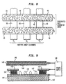
- FIG. 8 is a schematic diagram illustrating the conductor cathode array (vertical bands 90) together with crossing gate structures 91 with perforated gate holes 40 as described in application Serial No. 08/361616 filed December 22, 1994. The cross-point defines a pixel in the field emission display.
- FIG. 9 is a schematic cross section of a preferred field emission display using emitter-coated metal foil cathodes.
- the metal foil cathodes have a stripe configuration as shown in FIG. 2.
- the display comprises a metal foil cathode 141 of carbide-forming metal adhered to an insulating substrate 140 which is preferably glass.
- the foil 141 includes an adherent coating of low voltage diamond emitters 147 and an anode 145 disposed in spaced relation from the emitters within a vacuum seal.
- the foil preferably has a thickness of at least 0.02 mm.
- the anode conductor 145 formed on a transparent insulating substrate 146 is provided with a phosphor layer 144 and mounted on support pillars (not shown). Between the cathode and the anode and closely spaced from the emitters is a perforated conductive gate layer 143. Conveniently the gate 143 is spaced from the cathode 141 by a thin insulating layer 142.
- the space between the anode and the emitter is sealed and evacuated, and voltage is applied by power supply 148.
- the field-emitted electrons from electron emitters 147 are accelerated by the gate electrode 143 from multiple emitters 147 on each pixel and move toward the anode conductive layer 145 (typically transparent conductor such as indium-tin-oxide) coated on the anode substrate 146.
- Phosphor layer 144 is disposed between the electron emitters and the anode. As the accelerated electrons hit the phosphor, a display image is generated.
- metal foil cathode 141 can comprise nitride-forming metal and the electron emissive material can be AlN or AlGaN.
- the metal foil type conductor cathode array can also be used for non-display applications such as x-y matrix addressable electron sources or electron guns for electron beam lithography, microwave power amplifiers, ion guns, photocopiers and video cameras.
- the invention also applies to further modifications and improvements which do not depart from the spirit and scope of this invention.
Landscapes
- Engineering & Computer Science (AREA)
- Manufacturing & Machinery (AREA)
- Cold Cathode And The Manufacture (AREA)
- Cathode-Ray Tubes And Fluorescent Screens For Display (AREA)
- Devices For Indicating Variable Information By Combining Individual Elements (AREA)
Applications Claiming Priority (2)
| Application Number | Priority Date | Filing Date | Title |
|---|---|---|---|
| US08/555,594 US5648699A (en) | 1995-11-09 | 1995-11-09 | Field emission devices employing improved emitters on metal foil and methods for making such devices |
| US555594 | 1995-11-09 |
Publications (2)
| Publication Number | Publication Date |
|---|---|
| EP0773574A1 true EP0773574A1 (de) | 1997-05-14 |
| EP0773574B1 EP0773574B1 (de) | 2002-01-02 |
Family
ID=24217871
Family Applications (1)
| Application Number | Title | Priority Date | Filing Date |
|---|---|---|---|
| EP96307791A Expired - Lifetime EP0773574B1 (de) | 1995-11-09 | 1996-10-29 | Feldemissionsvorrichtungen mit Emittern auf Metallfolie und Verfahren zur Herstellung dieser Vorrichtungen |
Country Status (4)
| Country | Link |
|---|---|
| US (1) | US5648699A (de) |
| EP (1) | EP0773574B1 (de) |
| JP (1) | JP3455380B2 (de) |
| DE (1) | DE69618326T2 (de) |
Cited By (2)
| Publication number | Priority date | Publication date | Assignee | Title |
|---|---|---|---|---|
| WO1998027568A1 (en) * | 1996-12-18 | 1998-06-25 | Smiths Industries Public Limited Company | Diamond surfaces |
| US6040939A (en) * | 1998-06-16 | 2000-03-21 | Turkiye Sise Ve Cam Fabrikalari A.S. | Anti-solar and low emissivity functioning multi-layer coatings on transparent substrates |
Families Citing this family (32)
| Publication number | Priority date | Publication date | Assignee | Title |
|---|---|---|---|---|
| US6417605B1 (en) * | 1994-09-16 | 2002-07-09 | Micron Technology, Inc. | Method of preventing junction leakage in field emission devices |
| US5975975A (en) * | 1994-09-16 | 1999-11-02 | Micron Technology, Inc. | Apparatus and method for stabilization of threshold voltage in field emission displays |
| TW289864B (de) * | 1994-09-16 | 1996-11-01 | Micron Display Tech Inc | |
| US5637950A (en) * | 1994-10-31 | 1997-06-10 | Lucent Technologies Inc. | Field emission devices employing enhanced diamond field emitters |
| US5796211A (en) * | 1994-12-22 | 1998-08-18 | Lucent Technologies, Inc. | Microwave vacuum tube devices employing electron sources comprising activated ultrafine diamonds |
| CN1234134A (zh) * | 1996-10-17 | 1999-11-03 | 纳幕尔杜邦公司 | 纤维场致发射体的连接方法和用该方法制造的场致发射体阴极 |
| US6525461B1 (en) * | 1997-10-30 | 2003-02-25 | Canon Kabushiki Kaisha | Narrow titanium-containing wire, process for producing narrow titanium-containing wire, structure, and electron-emitting device |
| US6218293B1 (en) | 1998-11-13 | 2001-04-17 | Micron Technology, Inc. | Batch processing for semiconductor wafers to form aluminum nitride and titanium aluminum nitride |
| US6290564B1 (en) | 1999-09-30 | 2001-09-18 | Motorola, Inc. | Method for fabricating an electron-emissive film |
| US6469436B1 (en) * | 2000-01-14 | 2002-10-22 | Micron Technology, Inc. | Radiation shielding for field emitters |
| KR100436297B1 (ko) * | 2000-03-14 | 2004-06-18 | 주성엔지니어링(주) | 반도체 소자 제조용 플라즈마 스프레이 장치 및 이를이용한 반도체 소자 제조방법 |
| JP2001266737A (ja) * | 2000-03-24 | 2001-09-28 | Toshiba Corp | 電子源装置、その製造方法、および電子源装置を備えた平面表示装置 |
| US6387717B1 (en) * | 2000-04-26 | 2002-05-14 | Micron Technology, Inc. | Field emission tips and methods for fabricating the same |
| US6876724B2 (en) * | 2000-10-06 | 2005-04-05 | The University Of North Carolina - Chapel Hill | Large-area individually addressable multi-beam x-ray system and method of forming same |
| US6553096B1 (en) | 2000-10-06 | 2003-04-22 | The University Of North Carolina Chapel Hill | X-ray generating mechanism using electron field emission cathode |
| US7085351B2 (en) * | 2000-10-06 | 2006-08-01 | University Of North Carolina At Chapel Hill | Method and apparatus for controlling electron beam current |
| US7227924B2 (en) * | 2000-10-06 | 2007-06-05 | The University Of North Carolina At Chapel Hill | Computed tomography scanning system and method using a field emission x-ray source |
| US7082182B2 (en) * | 2000-10-06 | 2006-07-25 | The University Of North Carolina At Chapel Hill | Computed tomography system for imaging of human and small animal |
| US20050200261A1 (en) * | 2000-12-08 | 2005-09-15 | Nano-Proprietary, Inc. | Low work function cathode |
| US6885022B2 (en) * | 2000-12-08 | 2005-04-26 | Si Diamond Technology, Inc. | Low work function material |
| KR100571805B1 (ko) * | 2003-01-29 | 2006-04-17 | 삼성에스디아이 주식회사 | 전계방출소자와 이를 적용한 표시소자 및 그 제조방법 |
| JP4170172B2 (ja) * | 2003-08-21 | 2008-10-22 | ダイヤライトジャパン株式会社 | 照明装置 |
| JP2005174856A (ja) * | 2003-12-15 | 2005-06-30 | Toshiba Corp | シール材、およびシール材を用いた画像表示装置 |
| US8155262B2 (en) * | 2005-04-25 | 2012-04-10 | The University Of North Carolina At Chapel Hill | Methods, systems, and computer program products for multiplexing computed tomography |
| US8189893B2 (en) * | 2006-05-19 | 2012-05-29 | The University Of North Carolina At Chapel Hill | Methods, systems, and computer program products for binary multiplexing x-ray radiography |
| CN101842052B (zh) * | 2007-07-19 | 2013-11-20 | 北卡罗来纳大学查珀尔希尔分校 | 固定x射线数字化乳房断层合成系统和相关方法 |
| US8600003B2 (en) * | 2009-01-16 | 2013-12-03 | The University Of North Carolina At Chapel Hill | Compact microbeam radiation therapy systems and methods for cancer treatment and research |
| WO2011061208A1 (fr) * | 2009-11-18 | 2011-05-26 | Agc Glass Europe | Procede de fabrication d'un vitrage isolant |
| US8358739B2 (en) | 2010-09-03 | 2013-01-22 | The University Of North Carolina At Chapel Hill | Systems and methods for temporal multiplexing X-ray imaging |
| US9782136B2 (en) | 2014-06-17 | 2017-10-10 | The University Of North Carolina At Chapel Hill | Intraoral tomosynthesis systems, methods, and computer readable media for dental imaging |
| US10980494B2 (en) | 2014-10-20 | 2021-04-20 | The University Of North Carolina At Chapel Hill | Systems and related methods for stationary digital chest tomosynthesis (s-DCT) imaging |
| US10835199B2 (en) | 2016-02-01 | 2020-11-17 | The University Of North Carolina At Chapel Hill | Optical geometry calibration devices, systems, and related methods for three dimensional x-ray imaging |
Citations (9)
| Publication number | Priority date | Publication date | Assignee | Title |
|---|---|---|---|---|
| US4307507A (en) * | 1980-09-10 | 1981-12-29 | The United States Of America As Represented By The Secretary Of The Navy | Method of manufacturing a field-emission cathode structure |
| US4940916A (en) | 1987-11-06 | 1990-07-10 | Commissariat A L'energie Atomique | Electron source with micropoint emissive cathodes and display means by cathodoluminescence excited by field emission using said source |
| EP0411317A2 (de) * | 1989-06-28 | 1991-02-06 | Canon Kabushiki Kaisha | Verfahren und Vorrichtung zur kontinuierlichen Herstellung von funktionellen aufgedampften Filmen grosser Oberfläche mittels Mikrowellen-Plasma CVD |
| US5129850A (en) | 1991-08-20 | 1992-07-14 | Motorola, Inc. | Method of making a molded field emission electron emitter employing a diamond coating |
| US5138237A (en) | 1991-08-20 | 1992-08-11 | Motorola, Inc. | Field emission electron device employing a modulatable diamond semiconductor emitter |
| US5214347A (en) * | 1990-06-08 | 1993-05-25 | The United States Of America As Represented By The Secretary Of The Navy | Layered thin-edged field-emitter device |
| US5283500A (en) | 1992-05-28 | 1994-02-01 | At&T Bell Laboratories | Flat panel field emission display apparatus |
| US5396150A (en) * | 1993-07-01 | 1995-03-07 | Industrial Technology Research Institute | Single tip redundancy method and resulting flat panel display |
| EP0675519A1 (de) * | 1994-03-30 | 1995-10-04 | AT&T Corp. | Vorrichtung mit Feldeffekt-Emittern |
Family Cites Families (2)
| Publication number | Priority date | Publication date | Assignee | Title |
|---|---|---|---|---|
| US5290610A (en) * | 1992-02-13 | 1994-03-01 | Motorola, Inc. | Forming a diamond material layer on an electron emitter using hydrocarbon reactant gases ionized by emitted electrons |
| US5439753A (en) * | 1994-10-03 | 1995-08-08 | Motorola, Inc. | Electron emissive film |
-
1995
- 1995-11-09 US US08/555,594 patent/US5648699A/en not_active Expired - Lifetime
-
1996
- 1996-10-29 DE DE69618326T patent/DE69618326T2/de not_active Expired - Fee Related
- 1996-10-29 EP EP96307791A patent/EP0773574B1/de not_active Expired - Lifetime
- 1996-11-08 JP JP29558596A patent/JP3455380B2/ja not_active Expired - Fee Related
Patent Citations (10)
| Publication number | Priority date | Publication date | Assignee | Title |
|---|---|---|---|---|
| US4307507A (en) * | 1980-09-10 | 1981-12-29 | The United States Of America As Represented By The Secretary Of The Navy | Method of manufacturing a field-emission cathode structure |
| US4940916A (en) | 1987-11-06 | 1990-07-10 | Commissariat A L'energie Atomique | Electron source with micropoint emissive cathodes and display means by cathodoluminescence excited by field emission using said source |
| US4940916B1 (en) | 1987-11-06 | 1996-11-26 | Commissariat Energie Atomique | Electron source with micropoint emissive cathodes and display means by cathodoluminescence excited by field emission using said source |
| EP0411317A2 (de) * | 1989-06-28 | 1991-02-06 | Canon Kabushiki Kaisha | Verfahren und Vorrichtung zur kontinuierlichen Herstellung von funktionellen aufgedampften Filmen grosser Oberfläche mittels Mikrowellen-Plasma CVD |
| US5214347A (en) * | 1990-06-08 | 1993-05-25 | The United States Of America As Represented By The Secretary Of The Navy | Layered thin-edged field-emitter device |
| US5129850A (en) | 1991-08-20 | 1992-07-14 | Motorola, Inc. | Method of making a molded field emission electron emitter employing a diamond coating |
| US5138237A (en) | 1991-08-20 | 1992-08-11 | Motorola, Inc. | Field emission electron device employing a modulatable diamond semiconductor emitter |
| US5283500A (en) | 1992-05-28 | 1994-02-01 | At&T Bell Laboratories | Flat panel field emission display apparatus |
| US5396150A (en) * | 1993-07-01 | 1995-03-07 | Industrial Technology Research Institute | Single tip redundancy method and resulting flat panel display |
| EP0675519A1 (de) * | 1994-03-30 | 1995-10-04 | AT&T Corp. | Vorrichtung mit Feldeffekt-Emittern |
Cited By (2)
| Publication number | Priority date | Publication date | Assignee | Title |
|---|---|---|---|---|
| WO1998027568A1 (en) * | 1996-12-18 | 1998-06-25 | Smiths Industries Public Limited Company | Diamond surfaces |
| US6040939A (en) * | 1998-06-16 | 2000-03-21 | Turkiye Sise Ve Cam Fabrikalari A.S. | Anti-solar and low emissivity functioning multi-layer coatings on transparent substrates |
Also Published As
| Publication number | Publication date |
|---|---|
| JP3455380B2 (ja) | 2003-10-14 |
| DE69618326D1 (de) | 2002-02-07 |
| DE69618326T2 (de) | 2002-08-08 |
| EP0773574B1 (de) | 2002-01-02 |
| US5648699A (en) | 1997-07-15 |
| JPH09311644A (ja) | 1997-12-02 |
Similar Documents
| Publication | Publication Date | Title |
|---|---|---|
| EP0773574B1 (de) | Feldemissionsvorrichtungen mit Emittern auf Metallfolie und Verfahren zur Herstellung dieser Vorrichtungen | |
| US5977697A (en) | Field emission devices employing diamond particle emitters | |
| CA2166507C (en) | Field emission devices employing activated diamond particle emitters and methods for making same | |
| EP0709870B1 (de) | Verfahren und Vorrichtung zur Herstellung von teilchenförmigen und verbesserten Feldemittern und so erhaltene Produkte | |
| US6780075B2 (en) | Method of fabricating nano-tube, method of manufacturing field-emission type cold cathode, and method of manufacturing display device | |
| US5666025A (en) | Flat-panel display containing structure for enhancing electron emission from carbon-containing cathode | |
| US5729094A (en) | Energetic-electron emitters | |
| US20010004979A1 (en) | Field emission display and method for fabricating the same | |
| US6283812B1 (en) | Process for fabricating article comprising aligned truncated carbon nanotubes | |
| US20070103048A1 (en) | Method for fabricating carbon nanotube-based field emission device | |
| US6290564B1 (en) | Method for fabricating an electron-emissive film | |
| CA2166506C (en) | Improved field emission devices having corrugated support pillars with discontinuous conductive coating | |
| KR20010006238A (ko) | 전자 방출 소자 및 이의 제조 방법 | |
| KR100668332B1 (ko) | 카바이드 및 나이트라이드 나노 전자 에미터를 구비한 소자의 제조방법 | |
| US20090117811A1 (en) | Manufacturing method of electron-emitting device, manufacturing method of electron source, and manufacturing method of image display apparatus | |
| Reynolds et al. | Electron field emission from Ar+ ion-treated thick-film carbon paste | |
| Tang | Microelectronic applications for RF sources and accelerators | |
| Jung et al. | 8.2: Transformation of Electron Emission Behavior on Mo‐tip FEAs by Diamond‐Like Carbon Coating | |
| KR20070031831A (ko) | 전계 방출원 디바이스 | |
| JPH09330650A (ja) | 電子放出素子、それを用いた電子源、画像形成装置、及びそれらの製造方法 |
Legal Events
| Date | Code | Title | Description |
|---|---|---|---|
| PUAI | Public reference made under article 153(3) epc to a published international application that has entered the european phase |
Free format text: ORIGINAL CODE: 0009012 |
|
| AK | Designated contracting states |
Kind code of ref document: A1 Designated state(s): DE FR GB |
|
| 17P | Request for examination filed |
Effective date: 19971030 |
|
| 17Q | First examination report despatched |
Effective date: 19971216 |
|
| GRAG | Despatch of communication of intention to grant |
Free format text: ORIGINAL CODE: EPIDOS AGRA |
|
| GRAG | Despatch of communication of intention to grant |
Free format text: ORIGINAL CODE: EPIDOS AGRA |
|
| GRAH | Despatch of communication of intention to grant a patent |
Free format text: ORIGINAL CODE: EPIDOS IGRA |
|
| GRAH | Despatch of communication of intention to grant a patent |
Free format text: ORIGINAL CODE: EPIDOS IGRA |
|
| GRAA | (expected) grant |
Free format text: ORIGINAL CODE: 0009210 |
|
| REG | Reference to a national code |
Ref country code: GB Ref legal event code: IF02 |
|
| AK | Designated contracting states |
Kind code of ref document: B1 Designated state(s): DE FR GB |
|
| PG25 | Lapsed in a contracting state [announced via postgrant information from national office to epo] |
Ref country code: FR Free format text: LAPSE BECAUSE OF FAILURE TO SUBMIT A TRANSLATION OF THE DESCRIPTION OR TO PAY THE FEE WITHIN THE PRESCRIBED TIME-LIMIT Effective date: 20020102 |
|
| REF | Corresponds to: |
Ref document number: 69618326 Country of ref document: DE Date of ref document: 20020207 |
|
| PG25 | Lapsed in a contracting state [announced via postgrant information from national office to epo] |
Ref country code: GB Free format text: LAPSE BECAUSE OF NON-PAYMENT OF DUE FEES Effective date: 20021029 |
|
| EN | Fr: translation not filed | ||
| PLBE | No opposition filed within time limit |
Free format text: ORIGINAL CODE: 0009261 |
|
| STAA | Information on the status of an ep patent application or granted ep patent |
Free format text: STATUS: NO OPPOSITION FILED WITHIN TIME LIMIT |
|
| 26N | No opposition filed | ||
| PG25 | Lapsed in a contracting state [announced via postgrant information from national office to epo] |
Ref country code: DE Free format text: LAPSE BECAUSE OF NON-PAYMENT OF DUE FEES Effective date: 20030501 |
|
| GBPC | Gb: european patent ceased through non-payment of renewal fee |