EP0773591A2 - Lichtemittierende und lichtdetektierende Vorrichtung - Google Patents
Lichtemittierende und lichtdetektierende Vorrichtung Download PDFInfo
- Publication number
- EP0773591A2 EP0773591A2 EP96307962A EP96307962A EP0773591A2 EP 0773591 A2 EP0773591 A2 EP 0773591A2 EP 96307962 A EP96307962 A EP 96307962A EP 96307962 A EP96307962 A EP 96307962A EP 0773591 A2 EP0773591 A2 EP 0773591A2
- Authority
- EP
- European Patent Office
- Prior art keywords
- light
- photodiode
- module
- laser
- wavelength
- Prior art date
- Legal status (The legal status is an assumption and is not a legal conclusion. Google has not performed a legal analysis and makes no representation as to the accuracy of the status listed.)
- Withdrawn
Links
Images


Classifications
-
- H—ELECTRICITY
- H10—SEMICONDUCTOR DEVICES; ELECTRIC SOLID-STATE DEVICES NOT OTHERWISE PROVIDED FOR
- H10F—INORGANIC SEMICONDUCTOR DEVICES SENSITIVE TO INFRARED RADIATION, LIGHT, ELECTROMAGNETIC RADIATION OF SHORTER WAVELENGTH OR CORPUSCULAR RADIATION
- H10F55/00—Radiation-sensitive semiconductor devices covered by groups H10F10/00, H10F19/00 or H10F30/00 being structurally associated with electric light sources and electrically or optically coupled thereto
- H10F55/20—Radiation-sensitive semiconductor devices covered by groups H10F10/00, H10F19/00 or H10F30/00 being structurally associated with electric light sources and electrically or optically coupled thereto wherein the electric light source controls the radiation-sensitive semiconductor devices, e.g. optocouplers
- H10F55/25—Radiation-sensitive semiconductor devices covered by groups H10F10/00, H10F19/00 or H10F30/00 being structurally associated with electric light sources and electrically or optically coupled thereto wherein the electric light source controls the radiation-sensitive semiconductor devices, e.g. optocouplers wherein the radiation-sensitive devices and the electric light source are all semiconductor devices
Definitions
- This invention relates to a light emitting device/photodiode module which combines a plurality of photodiodes (PD) and laser diodes (LD) or light emitting diodes (LED) in an optical communication system which sends optical signals with different wavelengths in optical fibers bidirectionally between a broadcasting station and ONU terminals.
- PD photodiodes
- LD laser diodes
- LED light emitting diodes
- bidirectional optical communication The probability of a bidirectional optical communication system which enables two terminals to send the signals in both directions in a single fiber and to receive the signals from the counterpart at the same time.
- the system is called "bidirectional communication", because the fiber transmits the signals in both directions.
- the advantage of the system is that the signals can be sent by only a single fiber.
- Fig.1 shows the principle of a multiwavelength bidirectional optical communication system which utilizes different wavelengths of light.
- a central broadcasting station is combined by optical fibers with a plurality of terminals which are called an ONU (optical network unit).
- ONU optical network unit
- Fig.1 depicts only one terminal, there are a plenty of ONU terminals and a lot of bisectors in the fiber network.
- the signals from a broadcasting station travel in many fibers and bisectors to every one of the terminals.
- the broadcasting station amplifies digital signals of telephones and analog signals of televisions and drives a laser diode (LD1) with the amplified signals (P1).
- LD1 laser diode
- P1 amplified signals
- the optical signals of ⁇ 1 go into an optical fiber (1) and progress into a middle fiber (3) through the bisector (2). Travelling in the fiber (3), the ⁇ 1 signals arrive at a bisector (4) in an ONU module, and are guided into a fiber (5). Finally, the ⁇ 1 signals are transduced into electric signals (P3) by a photodiode (PD2) of the ONU terminal. The electric signals (P3) are amplified, processed and reproduced as voice of telephones or pictures of televisions on the ONU terminal. Such a signal which is sent from the broadcasting station to ONU terminals is called a "downward signal" and the direction of the flow is named a "downward direction”.
- an ONU converts the signals (P4) of telephones and facsimiles into light signals of a wavelength ⁇ 2 by a laser diode (LD2) in the ONU terminal.
- the ⁇ 2 signals enter a fiber (6), pass through the bisector (4) and propagate in the fiber (3) to the broadcasting station. Going through the bisector (2), the ⁇ 2 signals reach a photodiode (PD1) of the station.
- the photodiode (PD1) transduces the ⁇ 2 light signals into electric signals (P2) which is fed into a converter, a processor or so.
- Such a signal which is transmitted from an ONU to the broadcasting station is called an "upward signal".
- the direction of the signal flow is named an "upward direction”. Since the fiber (3) allows light signals to travel in both directions, the system can be called a "bidirectional communication system".
- the above system uses the ⁇ 1 light only for the downward signals and the ⁇ 2 light exclusively for the upward signals. It is, however, also possible to make use of the same wavelength both for the upward signals and the downward signals. Sometimes both wavelengths are commonly used both for the upward signals and the downward signals. In the modes which send the same wavelength light bidirectionally, one of the most important problems is the separation of the light of different wavelengths travelling in the same direction.
- the bidirectional communication system which sends optical signals of two different wavelengths in a single fiber both in the downward direction and in the upward direction requires devices for distinguishing the light signals with the different wavelengths both at the broadcasting station and at the ONU terminals.
- the WDM (2)(wavelength division multiplexer) at the broadcasting station and the WDM (4) at the ONUs in Fig.1 play the role of distinguishing and separating the light waves of the different wavelengths.
- the WDM has a function of selecting one of two different wavelengths in an input fiber and guiding the selected wavelength into an output optical fiber and another function of integrating the light waves of two different wavelengths ⁇ 1 and ⁇ 2 travelling in two fibers into an optical fiber.
- the WDM plays an important role in the multiwavelength bidirectional communication.
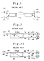
- Fig.2 to Fig.4 exhibit some of the proposed WDMs.
- Fig.2 denotes a WDM made of optical fibers or optical waveguides.
- Two optical paths (8) and (9) join together at a part (10) at which two paths exchange energy with each other.
- Various modes of coupling are realized by selecting the spacing (D) or the length (L) of the closing part (10).
- the WDM combines the ⁇ 1 light in the path (8) and the ⁇ 2 light in the path (9) and introduces both the ⁇ 1 light and the ⁇ 2 light together into a path (11) to a port (P3). Neither the ⁇ 1 nor the ⁇ 2 goes into the path (12).
- ⁇ 1 does not transfer into the neighboring path and remains in the original fiber but ⁇ 2 fully transfers into the other path.
- the WDM made of fibers or waveguides has an advantage of little dependence on the polarization of light waves, since the WDM is made from optical fibers or optical waveguides.
- the optical paths in waveguides or fibers have reversibility with regard to the direction of propagation.
- the WDM shown in Fig.2 can be used as a bidirectional WDM indicated by Fig.3 in the bidirectional network.
- the WDM introduces the ⁇ 1 light into a fiber (8) from a port (P1) and guides the light to go out through a fiber (11) to a port (P3).
- the same WDM receives the ⁇ 2 light from the port (P3) and supplies the ⁇ 2 light to the port (P2).
- the WDM can be utilized as the WDM in Fig.1.
- Fig.4 exhibits another WDM making use of dielectric multilayers.
- the dielectric type WDM has two transparent isosceles rectangular triangle columns (13) and (14) and a dielectric multilayer (15) coated on the bisecting plane of the column.
- the multilayer (15) reflects the whole of the ⁇ 2 light but makes all the ⁇ 1 light pass through by adjusting the refractive indices and the thicknesses of the dielectric films.
- the dielectric multilayer type WDM has a dependence upon the polarization, since the selective mirror (15) reflects or permits the beams which collide with the mirror surface at 45 degrees.
- the dielectric multilayer WDM can also be adopted as the WDMs in the network system in Fig.1. Such a WDM has been on sale.
- a laser/photodiode module on an ONU terminal is now explained by referring to Fig.5.
- An end of the fiber (16) leading to a central broadcasting station (not shown) is joined to an inner optical fiber (18) via an optical connector (17).
- An ONU module in the house of the CATV subscriber has an optical fiber WDM (21) which connects the fiber (18) to a fiber (19) at a joint (20) with wavelength selectivity.
- the fiber (18) is connected to an LD (laser diode) module (25) of 1.55 ⁇ m via a connector (22) and a fiber (24).
- Another fiber (19) communicates with a PD (photodiode) module (27) via a connector (23) and a fiber (26).
- the LD (25) and the fiber (24) build an upward system for sending the signals of 1.55 ⁇ m light from the ONU terminal to the broadcasting station.
- the PD (27) and the fiber (26) construct a downward system for receiving the signals of 1.3 ⁇ m light from the broadcasting station.
- the PD (27) converts the 1.3 ⁇ m optical signals into electric signals in the ONU module.
- the LD module (25), a transmitter includes the devices for amplifying the signals of telephones and facsimiles, modulating the electric signals by some mode and a laser for transducing the electric signals into optical signals.
- the PD module (27) contains a photodiode for converting the optical signals of TV or telephones from the broadcasting station to electric signals, an amplification circuit and a demodulation circuit.
- the WDM (21) has a function of separating the 1.55 ⁇ light from the 1.3 ⁇ m light.
- the present system allocates the 1.55 ⁇ m light to the upward system and the 1.3 ⁇ m light to the downward system.
- the downward system requires two different wavelengths. One wavelength must be used both in the downward system and in the upward system. Thus, the WDM must separate two different wavelengths with a high efficiency.
- Fig.34 Another example of prior PD/LD module on an ONU terminal is exhibited by Fig.34.
- This module is simply obtained by exchanging the wavelengths of 1.3 ⁇ m and 1.55 ⁇ m in the mentioned one of Fig.5.
- a fiber (226) from the central station is coupled to an inner fiber (228) by an optical connecter (227).
- a fiber-type WDM (231) separates the light by the wavelength into 1.3 ⁇ m and 1.55 ⁇ m light spatially. As mentioned before, the distance D and the length L of the WDM determine the wavelengths to be allocated to two paths.
- the WDM (231) allots the 1.3 ⁇ m light to a fiber (228). 1.55 ⁇ m light is allotted to another fiber (229).
- the fiber (228) is joined to an LD module (235) by a connector (232).
- the LD (235) module converts digital signals of the ONU terminal into light signals and sends the optical signal to the central station.
- the fiber (229) is coupled by a connector (233) to a PD module (237) which transduces the optical signals sent from the station to electric signals.
- This invention relates to an improvement of a laser/photodiode (LD/PD) module for a bidirectional optical communication system by the light of two wavelengths.
- the laser/photodiode module includes a laser diode, a photodiode and electric circuits for supporting the transducers. Prior art for the parts is explained.
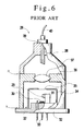
- FIG.6 A prior semiconductor light emitting device (28) is now explained by referring to Fig.6.
- This is a laser module containing a laser chip (29) and a photodiode chip (30) for monitoring the output of the laser (29).
- the semiconductor laser diode chip (29) is mounted on a vertical wall of a protrusion (31) of a header (32), because the laser (29) emits light in the direction parallel to the surface.
- the monitoring photodiode (30) is mounted on an insulating submount bonded on the header (32). The light emitted from the bottom end of the laser (29) is detected by the photodiode (30).
- a plural lead pins (33) are implanted on the bottom of the header (32).
- the upper surface of the header (32) is covered by a cap (34).
- the cap (34) has an opening (35) at the center of the upper wall.
- the laser emits light upward and downward.
- a lens (37) is upholstered just above the opening (35).
- a cylindrical lens holder (36) holds the lens (37).
- a conical housing (38) is welded on the lens holder (36). The top of the housing (38) maintains a ferrule (39) which fixes an end of an optical fiber (40). Ends of the ferrule (39) and the optical fiber (40) are ground in a slanting plane at an angle of e.g., 8 degrees. The slanting end of the fiber prevents the reflected light from returning the laser diode (29).
- the lens holder (36) is welded at the periphery (A) on the header (32) at the optimum position in which the lens axis coincides with the laser optical axis in the vertical direction. Then the housing (38) is positioned and welded on the holder (36) at the position which maximizes the output from the other end of the fiber (40). Every electrode pad of the laser chip (29) and the photodiode chip (30) is wirebonded to any of the lead pins (33) of the header (32). The light beams emitted from the laser (29) are converged to an end of the fiber (40) by the lens (37). The light beams bring optical signals, because the laser (29) is modulated by the electric signals. The output of the laser (29) is monitored by the photodiode (30). The wavelength of the light is determined by the material of the semiconductor layers of the laser (29).
- FIG.7 demonstrates an example of a prior photodiode module.
- a photodiode chip (41) is die-bonded on a header (42).
- the header (42) has lead pins (43) on the bottom.
- a cap (44) is fitted on the top surface of the header (42).
- the cap (44) has an opening (45) at the center.
- a cylindrical holder (46) is fixed on the header (42) for supporting a lens (47).
- a conical housing (48) is fixed on the lens holder (46).
- the housing (48) sustains a ferrule (49) holding an end of an optical fiber (50).
- the ends (51) of the ferrule (49) and the fiber (50) are cut in a slanting plane.
- the positions of the holder (46), the housing (48) and the ferrule (49) are determined at the positions which maximize the output of the photodiode, when light is led into the other end of the fiber (50).
- the material of the light receiving layer of the photodiode determines the range of the wavelength of the light detectable by the PD.
- a Si photodiode is available for sensing visible light.
- a Si photodiode is unsuitable, since the present invention aims at an improvement of an ONU module which adopts near-infrared light for which a Si PD has no sensitivity.
- the optical communication requires a compound semiconductor photodiode having an InP substrate for sensing the infrared light.
- FIG.8 is a section of a prior PD chip employed by the optical communication system.
- the substrate (52) of the PD chip is n-InP.
- An n-InP buffer layer (53), an n-InGaAs light receiving (absorbing) layer (54) and an n-InP window layer (55) are epitaxially grown in this order on the n-InP substrate (52).
- a p-region (56) is made at the center of the top surface by diffusing zinc (Zn) through a mask. The region of Zn-diffusion attains to some part of the n-InGaAs light receiving layer (54).
- the p-region (56) includes the p-InP window layer and the p-InGaAs light receiving layer. Namely, a pn-junction is formed in the InGaAs absorption layer.
- a ring p-electrode (57) is formed on the Zn-diffusion region (56). Light enters the photodiode chip at an inner part enclosed by the annular p-electrode (57). The inner part within the p-electrode (57) is covered with an antireflection film (58). The outer part of the window layer (55) is protected with a passivation film (59).
- An n-electrode (61) is formed on the bottom of the n-InP substrate (52).
- the whole bottom of the chip is fully covered with the n-electrode (61) in prior photodiodes. This is one of the features of prior PDs.
- the pn-junction is reversely biased by applying voltage between the p-electrode (57) and the n-electrode (61).
- the light (60) going out of the optical fiber passes the central antireflection film (58), the p-InP window layer, p-InGaAs layer, the pn-junction and the n-InGaAs layer (54).
- the light is absorbed in the vicinity of the pn-junction. The absorbed light generates pairs of electrons and holes.
- the photodiode Since the photodiode is reversely biased, the electrons run toward the n-electrode (61) and the holes progress to the p-electrode (57). A photocurrent flows in the PD chip. Since the number of photons is in proportion to the photocurrent, the PD can detect the amount of the incident light power.
- the InGaAs light receiving layer absorbs both 1.3 ⁇ m light and 1.55 ⁇ m light.
- the InP window layer absorbs neither 1.3 ⁇ m light nor 1.55 ⁇ m light.
- a semiconductor permits the light of an energy h ⁇ less than the energy gap Eg (h ⁇ ⁇ Eg) to pass through without loss, because the photon energy h ⁇ cannot excite the electrons in the valence band up to the conduction band.
- a semiconductor is transparent for the light of a wavelength ⁇ longer than the edge wavelength hc/Eg corresponding to the band gap energy Eg.
- a semiconductor absorbs all the light of a wavelength shorter than the edge wavelength hc/Eg, if the semiconductor has an enough thickness, because the photons (h ⁇ > Eg) can excite the electrons in the valence band up to the conduction band.
- Egw denotes the band gap energy of the InP window layer.
- Egz is the band gap of the InGaAs absorption layer.
- the light having an intermediate energy h ⁇ of Egz ⁇ h ⁇ ⁇ Egw passes the window layer but is entirely absorbed in the absorbing layer.
- the photodiode can detect only the light having an energy h ⁇ which is bigger than Egz but smaller than Egw.
- the range of the detectable wavelength ⁇ is hc/Egw ⁇ ⁇ ⁇ hc/Egz.
- the components of the absorption layer (54) is simply represented as InGaAs without a ratio x of a mixture crystal.
- the ratio x defining the component of In 1-x Ga x As is uniquely determined by the condition of the lattice fitting of In 1-x Ga x As to InP.
- the band gap of the InGaAs absorption layer is determined without ambiguity.
- Fig.9 shows the sensitivity as a function of the wavelength of the conventional photodiode of Fig.8.
- the abscissa is the wavelength ⁇ ( ⁇ m) of the incident light.
- the ordinate is the sensitivity (A/W).
- the sensitivity is low for the wavelength below 0.95 ⁇ m (P-point).
- the range (Q-region) from 1.0 ⁇ m to 1.5 ⁇ m enhances the sensitivity linearly.
- At 1.7 ⁇ m (R-point) the sensitivity falls rapidly.
- the sensitivity reduces to 0.
- the band gap Egw of the window layer determines the sensitivity-rising point P.
- the band gap Egz of the absorption layer determines the sensitivity-falling point R.
- the prior InGaAs photodiode has a wide range of sensitivity including 1.3 ⁇ m and 1.55 ⁇ m. Therefore, the same InGaAs photodiode can be used both for detecting 1.3 ⁇ m light and for sensing 1.55 ⁇ m light.
- a photon creates a pair of an electron and a hole which originates a photocurrent of q (q is an elementary charge) in an ideal case with a conversion efficiency of 100%. If the conversion efficiency were 100%, the sensitivity should be given by q ⁇ /hc (A/W). The fact causes the linear rise of the sensitivity in the Q-region between 1.0 ⁇ m and 1.55 ⁇ m.
- a high-performance photodiode has such a sensitivity curve. Apparently, it seems convenient to use a wide-range photodiode which can sense both 1.3 ⁇ m light and 1.55 ⁇ m light in the multiwavelength communication system employing 1.3 ⁇ m and 1.55 ⁇ m. The selection of the wide-range photodiode, however, incurs a serious problem.
- the other problem is the existence of WDMs (wavelength division multiplexers) in the ONU terminals and the broadcasting station.
- the conventional ONU terminals require WDMs for separating spatially the light waves of different wavelengths.
- the conventional WDMs of optical fiber type, waveguide type or dielectric mirror type can deal with only two different wavelengths. No current WDM can separate the light waves of more than two wavelengths.
- These WDMs introduce one wavelength into an optical path and the other wavelength into another path by transcribing the difference of the wavelengths to the difference of the phase constants ⁇ , and separating one wavelength from the other wavelength spatially.
- the WDMs allocate two different wavelength waves in a rate of 1:1.
- the conventional WDMs cannot separate three different wavelengths. Namely, the system based on the WDMs is incapable of treating with the multiwavelength containing more than two wavelengths.
- WDMs suffer from another defect of imperfection of spatial separation.
- Two outputs are now denoted by the output 1 and the output 2.
- ⁇ is called an extinction ratio.
- ⁇ 0 of course.
- the extinction ratio must be smaller than 1/10000 for separating two wavelengths without cross-talk.
- dielectric multilayer films are sometimes used further to decrease the extinction rate ⁇ .
- Multiwavelength PD modules without a WDM have been suggested for avoiding the difficulty of the definite ⁇ .
- 1Japanese Patent Laying Open No.6-45635(No.45635/'94) proposed a PD module having two PDs on the same chip which have sensitivity for both two different wavelengths ⁇ 1 and ⁇ 2, two filters which admit one of ⁇ 1 and ⁇ 2 to penetrate.
- the device has a parallel arrangement of PDs.
- the existence of two parallel PDs dispenses with WDMs.
- the extinction ratio of the wavelength filter is still not satisfactory yet.
- Such a parallel selective PD device cannot entirely separate and sense the light waves of two different wavelengths.
- the device has a more serious drawback that the input power is too weak, since the power is divided into three or two parts. Such a weak input power reduces the sensitivity.
- a horizontal type photodiode (waveguide type) which senses only the light with a certain wavelength has also been proposed. The photodiode has been investigated and produced tentatively for detecting the light of one wavelength which is separated by a WDM.
- This photodiode has been developed as a photodiode for detecting only 1.3 ⁇ m, after 1.3 ⁇ m and 1.55 ⁇ m have been separated by a WDM.
- the photodiode demands a WDM of course.
- a large reflection loss at the end reduces the quantum efficiency of the photodiode to about 36%.
- a prior LD/PD module consists of three important parts; a WDM, a laser and a photodiode.
- the large number of the parts raises the cost of the module.
- This is a large drawback as a LD/PD module for the bidirectional optical communication system.
- Another weak point is a large power loss at the joints of optical fibers and WDMs.
- the prior LD/PD modules have been applied only to a short range communication system.
- One purpose of the present invention is to provide a LD/PD module which is built with a smaller number of parts. Another purpose of the present invention is to provide a smaller size LD/PD module produced at a lower cost. Another purpose of the present invention is to provide a LD/PD module with a lower loss of light. Another object of the present invention is to provide a LD/PD module feasible to a long range optical communication. Another purpose of the present invention is facilitating the pervasion of optical subscriber network by proposing LD/PD modules of low cost and low loss. The further purpose of the present invention is to provide a LD/PD module suitable to multiwavelength bidirectional optical communication adopting more than two different wavelengths.
- prior LD/PD modules intended to separate the light beams of different wavelengths spatially without exception.
- the prior LD/PD modules became large, bulky devices because of the spatial separation of the beams.
- the spatial separation of different wavelengths is still not perfect.
- the defective separation of wavelengths brought about a large loss.
- the spatial separation is equivalent to the wavelength separation in all the prior devices. If the spatial separation is imperfect, the wavelength separation becomes defective.
- the imperfection of the wavelength separation invites the problem of cross-talk. In the case of TV signals, flickers appear on the screen due to the fault of wavelength separation.
- An enhancement of the spatial separation requires more sophisticated, expensive WDMs, which increase the size and the cost of the module.
- the Inventors thought of a new idea of receiving the light of different wavelengths through the same path without separating spatially the paths in contradiction to the prior ones.
- This invention does not divide the optical paths for different wavelengths but guides all the wavelengths in the same straight path and detects the different wavelengths at different spots on the same path. If such a "linear detection" is possible, the device would be immune from the problem of the spatial separation and the problem of the cross-talk due to the imperfection of the spatial separation. Is the linear detection truly possible?
- Prior LD/PD modules have already utilized wide range photodiodes which sense all the wavelengths included in the signals. Namely, prior modules have adopted general-purpose photodiodes. This is an origin of the serious problems of the prior modules. Since the photodiodes have sensitivity to all the light waves included in the signals, WDMs or dielectric multilayers were indispensable for separating spatially the signals by wavelengths. The prior modules separated the different wavelengths, guided the light of the different wavelengths into different paths having a general-use PD at the end and detected the power of the light of the respective wavelengths by the common-use end PDs.
- the present invention does not employ such wide range sensitive general-purpose photodiodes but adopts narrow range sensitive photodiodes which are novel enough themselves. Namely, the present invention uses a special-use, narrow range sensitive photodiode Dj which can sense only ⁇ j. Expensive WDMs are excluded from the present invention. The same function as WDMs is carried out by a set of the narrow range sensitive photodiodes. Thus, the module of the invention dispenses with WDMs.
- the present invention is based upon the profound consideration over the physics of the semiconductors of photodiodes. The inventors thought of a method of making a photodiode which can sense only a single wavelength.
- Fig.29 shows the relation between the energy of the incident light and the band structure of semiconductor in a photodiode.
- Ec denotes the energy of the bottom of the conduction band.
- Ev indicates the energy of the top of the valence band.
- the difference is the band gap Eg of the semiconductor.
- Eg Ec-Ev.
- the intermediate part between the conduction band and the valence band is called a forbidden band (forbidden gap). There is no electron level in the forbidden band (forbidden gap),if the semiconductor includes no impurity. A little electrons exist in the conduction band.
- the valence band is nearly filled with electrons.
- the deficiencies of electrons in the valence band is named holes.
- the electron concentration is 0 in the conduction band and the hole concentration is 0 in the valence band.
- the forbidden band forbidden gap
- the Fermi level is just at the middle in the forbidden band (forbidden gap). Electrons are excited in the conduction band and holes are excited in the valence band by heat at a definite temperature.
- a photon When light enters semiconductor, a photon (quantum of light) raises an electron of the valence band up to the conduction band.
- the phenomenon is named an excitation of a pair of an electron and a hole.
- the light (h ⁇ ⁇ Eg) passed the semiconductor without loss.
- the semiconductor is transparent for the light of h ⁇ ⁇ Eg (or ⁇ ⁇ ⁇ g).
- n-type semiconductor makes shallow donor levels En and a p-type semiconductor makes shallow acceptor levels Ep in the forbidden band (forbidden gap).
- Fig.30 shows the impurity levels in an n-type semiconductor or in a p-type semiconductor. Due to the existence of the impurity levels, the limit for permitting the transition is lowered from Eg to (Eg-En) or (Eg-Ep). The shallow levels En or Eg are about one hundredth to one tenth. Thus, the same matter occurs also in n-type semiconductors or p-type semiconductors except replacing Eg by (Eg-En) or (Eg-Ep). Such an impurity which makes a deep level Es is not doped for controlling the conduction property. A good epitaxial layer has no deep impurity level. The actual values of (Eg-En) or (Eg-Ep) are nearly equal to Eg.
- the photons of energy higher than the band gap Eg (E ⁇ Eg: ⁇ ⁇ ⁇ g) are absorbed.
- the photons of an energy lower than Eg (E ⁇ Eg: ⁇ > ⁇ g) pass the semiconductor.
- a semiconductor has an intrinsic wavelength selectivity.
- the present invention takes advantage of the wavelength selectivity of semiconductors. This invention proposes a new device which makes the best use of the wavelength selectivity of semiconductors.
- a photodiode can be regarded as a set of an absorption layer (Egz) and a window layer (Egw) (Egz ⁇ Egw).
- the light of energy lower than Egw passes the window layer.
- the light of energy higher than Egz is absorbed by the absorption layer (light receiving layer).
- the other light of energy lower than Egz penetrates through the absorption layer but absorbed and annihilated by the n-electrode (61) in Fig.8. Namely, the incident light can be classified into three different types by the energy.
- the band gap Egw of the window layer What defines the upper limit R is the band gap Egz of the light receiving (absorbing) layer. In any PD, Egz ⁇ Egw.
- the photodiode senses all the light of a wavelength between Egz and Egw. If the difference (Egw-Egz) is reduced to an enough small value, the photodiode senses only the light of a narrow range Em of energy, where Egz ⁇ Em ⁇ Egw.
- a narrow range sensitive photodiode can be built by selecting the materials of the window layer and the absorption layer for nearly equalizing Egz up to Egw.
- the photodiode can detect only the light of ⁇ m which satisfies the inequality ⁇ w ⁇ ⁇ m ⁇ ⁇ z.
- the difference (Egz-Egw) is decreased to a small value, the photodiode becomes a narrow range sensitive, specialized photodiode.
- a photodiode is now specified by the edge wavelength ⁇ w of a window layer and the edge wavelength ⁇ z of an absorption layer.
- a photodiode is written as D( ⁇ w, ⁇ z). The symbol D( ⁇ w, ⁇ z) means that the photodiode has sensitivity only for ⁇ of ⁇ w ⁇ ⁇ ⁇ z.
- a set of narrow-range sensitive photodiodes D1( ⁇ w1, ⁇ z1), D2( ⁇ w2, ⁇ z2), D3( ⁇ w3, ⁇ z3), ⁇ and Dn( ⁇ wn, ⁇ zn) can be designed for detecting only the counterpart wavelength ⁇ 1, ⁇ 2, ⁇ 3, ⁇ or ⁇ n respectively by determining the materials of the window layers and the receiving layers as follows.
- D1( ⁇ w1, ⁇ z1) ⁇ w1 ⁇ ⁇ 1 ⁇ ⁇ z1 ⁇ ⁇ 2.
- D2( ⁇ w2, ⁇ z2) ⁇ 1 ⁇ ⁇ w2 ⁇ ⁇ 2 ⁇ ⁇ z2 ⁇ ⁇ 3.
- D3( ⁇ w3, ⁇ z3) ⁇ 2 ⁇ ⁇ w3 ⁇ ⁇ 3 ⁇ ⁇ z3 ⁇ ⁇ 4.
- Dj( ⁇ wj, ⁇ zj) ⁇ j-1 ⁇ ⁇ wj ⁇ j ⁇ ⁇ zj ⁇ ⁇ j +1.
- Dn( ⁇ wn, ⁇ zn) ⁇ n-1 ⁇ ⁇ wn ⁇ ⁇ n ⁇ ⁇ zn.
- the inequality ⁇ wj ⁇ ⁇ j ⁇ ⁇ zj is the requirement for sensing the ⁇ j light by photodiode Dj. Attention should be paid to the inequalities on both sides.
- ⁇ j-1 ⁇ ⁇ wj and ⁇ zj ⁇ ⁇ j +1 signify that Dj is fully insensitive to the neighboring the ⁇ j-1 light or the ⁇ j+1 light.
- photodiode Dj is defined by a positive condition of sensing ⁇ j and a negative condition of being insensitive to the neighboring ⁇ j-1 and ⁇ j+1 light. Namely, the sensitivity curves of the neighboring photodiodes do not overlap.
- n photodiodes do not overlap in the sensitivity curves.
- the sensitivity curves are all independent and isolated from each other.
- Such a narrow-range photodiode Dj can be called an eigen-wavelength photodiode.
- Eigen-wavelength photodiodes play an important role in the present invention.
- This invention proposes a novel photodiode which permits the light of wavelengths higher than ⁇ z to pass through the bottom without being blocked.
- a photodiode can be produced by replacing the conventional overall bottom electrode (61) by a ring electrode, coating the revealed substrate bottom with a transparent protection film.
- a photodiode may be named a "transmission type" photodiode.
- Adoption of the transmission type photodiodes is the other feature of the present invention. One condition was the "eigen-wavelength" character of photodiodes.
- the photodiode this invention utilizes is an eigen-wavelength, transmission type photodiode.
- the feature of the photodiode of the invention is then expressed by an eigen-wavelength, transmission type photodiode.
- the conventional PD may be called a common-wavelength, blocking type photodiode.
- This invention builds a novel, linear LD/PD module for multiwavelength optical fiber communication by aligning a plurality of eigen-wavelength, transmission type photodiodes in series in the order of increasing eigen wavelengths. Since the whole photodiodes align along a straight line, the same light passes the series of the photodiodes one by one. Each of the wavelengths is detected and fully absorbed by the eigen PD. All the wavelengths are detected by the set of photodiodes arranged on a direct line. All the prior multiwavelength modules intended to separate wavelengths spatially by WDMs. The prior modules are called a parallel detection type. The present invention may be called a serial detection type module in contrast to the prior ones. Then the modules of the invention are called "linear modules".
- the group of the photodiodes requires a special algebra.
- the signal light is denoted by "S”.
- the signal S including n wavelengths ⁇ 1, ⁇ 2, ⁇ 3, ⁇ , ⁇ n is written as S(n: ⁇ 1, ⁇ 2, ⁇ 3, ⁇ , ⁇ n).
- the wavelengths are arranged in the increasing order ( ⁇ 1 ⁇ ⁇ 2 ⁇ ⁇ 3 ⁇ ⁇ ⁇ ⁇ n).
- a photocurrent is denoted by I. If the photocurrent I includes m wavelengths ⁇ 1, ⁇ 2, ⁇ 3, ⁇ , ⁇ m ( ⁇ 1 ⁇ ⁇ 2 ⁇ ⁇ 3 ⁇ ⁇ ⁇ ⁇ m), the photocurrent is indicated by I (m: ⁇ 1, ⁇ 2, ⁇ 3, ⁇ , ⁇ m). If a mixture of a plurality of wavelengths is converted into a photocurrent I at the same device, cross-talk occurs. This invention succeeds in avoiding an occurrence of cross-talk which is caused by a mixture of more than one wavelength in a photocurrent by allocating a wavelength to an eigen photodiode. Every photodiode senses only one wavelength in the signals. The j-th PD originates only a simple photocurrent I(1: ⁇ j) in the present invention.
- the photodiode plays the role of receiving an input optical signal S and making outputs of S+I. Or the PD can be deemed an operator of converting an input S into output S+I.
- An output of the PD is given by (input) ⁇ (PD operator) in the photodiode algebra. Unlike ordinary mathematics, an operator acts upon the value on the left side for facilitating to compare the equations with the drawings in the algebra.
- "D" is the operator of a photodiode.
- the first problem is what expression the algebra gives to the prior PD. [For prior PDs] The prior wide-range, common wavelength type PD will give an expression for the light signals including a plurality of wavelengths.
- the j-th PD senses only the j-th wavelength ⁇ j, absorbs all the light of (j-1) wavelengths shorter than ⁇ j and permits the rest of (n-j) wavelengths longer than ⁇ j to pass through. The rest can be an input for the next (j+1)-th photodiode.
- Dj is an operator for the j-th PD. But the j-th PD is sometimes represented by Dj hereinafter for brevity.
- Dj( ⁇ wj, ⁇ zj) is the operator of the j-th PD.
- S(n: ⁇ 1, ⁇ 2, ⁇ 3, ⁇ , ⁇ n) means that the light including n different wavelengths is introduced into the j-th PD.
- 1(1: ⁇ j) is a photocurrent of the j-th wavelength produced by the j-th PD.
- S(n-j: ⁇ j+1, ⁇ j+2, ⁇ , ⁇ n) indicates that (n-j) wavelengths higher than ⁇ j go out of the j-th PD without being absorbed.
- Eq.(8) is meaningless.
- Eq.(9) is important.
- Eq.(9) says that if two photodiodes Dj and Dk with a relation of j ⁇ k are aligned in this order, the conjunction can sense individually ⁇ j and ⁇ k and can give an optical output comprising ⁇ k+1, ⁇ K+2, ⁇ , ⁇ n from the bottom of Dk.
- the difference between Eq.(8) and Eq.(9) means that the operators Dk and Dj are not commutative.
- Eq.(9) teaches us that if plural PDs are joined in series in the order of wavelengths, respective wavelengths can be independently sensed by the PDs in charge.
- the best module can be produced by aligning photodiodes D1, D2, D3, ⁇ , Dn in series in the order of increasing wavelengths ( ⁇ 1 ⁇ ⁇ 2 ⁇ ⁇ 3 ⁇ ⁇ ⁇ ⁇ n).
- the output includes all the photocurrents of the signals carried by the different wavelengths independently.
- Eq.(10) says that when photodiodes are joined in series in the order of enhancing the wavelengths, all the photodiodes can sense their eigen wavelengths independently.
- S(1,2, ⁇ ,n) is a simplification of S(n: ⁇ 1, ⁇ 2, ⁇ 3, ⁇ , ⁇ n).
- D1 is a simplified operator of D1( ⁇ w1, ⁇ z1).
- I1 is an abbreviation of I(1: ⁇ 1).
- two operators Dj and Dk are incommutative.
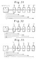
- Fig.31 demonstrates the linear conjunction of plural photodiodes expressed by Eq.(11) or Eq.(12).
- the eigen-wavelength, transmission type photodiodes are arranged in a linear conjunction in the order of D1, D2, D3, ⁇ and Dn.
- signals S including the wavelengths ⁇ 1, ⁇ 2, ⁇ 3, ⁇ 4, ⁇ , ⁇ n is introduced in the series conjunction of photodiodes, D1 detects only ⁇ 1, D2 senses only ⁇ 2, D3 feels only ⁇ 3, ⁇ and Dn senses only ⁇ n.
- horizontal arrows ⁇ 1, ⁇ 2, ⁇ 3, ⁇ , ⁇ j, ⁇ , ⁇ n show the distance at which the wavelengths arrive.
- the upward arrows indicate the photocurrents of ⁇ 1, ⁇ 2, ⁇ , ⁇ j, ⁇ , ⁇ n converted by photodiodes D1, D2, ⁇ ,Dj, ⁇ and Dn.
- a straight light path is formed through a series of photodiodes and the wave of a longer wavelength goes further in the linear conjunction of PDs.
- the above is an improvement of a PD module having a series conjunction of plural photodiodes. Since photodiodes are passive devices, linearly jointed photodiodes can deduce their eigen wavelengths without interference.
- the thought of the present invention is not solely restricted within an improvement of an assembly of photodiodes.
- This invention can be extended to an improvement of a module including a light emitting device. Namely, this invention is capable of applying to a PD/LD module.
- the light emitting device means a light emitting diode or a laser diode.
- the wavelength ⁇ q of emanating light is determined by the band gap Eg of the emanating layer.
- a PD/LD module of the present invention is built by adding a light emitting device at an end of a series of photodiodes.
- the PD/LD module consists of a linearly joined (n-1) photodiodes and an n-th light emitting device Ln.
- the module has a linear junction of SD1D2D3Dn-1Ln.
- the emission wavelength ⁇ n of the final light emitted device Ln is longer than the longest one among the eigen wavelengths of the photodiodes D1 to Dn-1, the light emanating from the end light emitting device can progress through all the preceding photodiodes without loss.
- the direction of the light from the end light emitting device is inverse to the signal light.
- Fig.33 demonstrates the structure of the PD/LD module of this invention. Initially, the signal S includes (n-1) wavelengths ⁇ 1, ⁇ 2, ⁇ 3, ⁇ , ⁇ (n-1) which are all absorbed by the preceding (n-1) photodiodes.
- the final light emitting device is not affected by the input signals.
- the PD/LD module has a single laser diode at the end of the series of PDs.
- the linear module forbids more than one laser to follow the series of photodiodes. The reason is an occurrence of interference between two lasers. If two lasers were allotted at the j-th seat and the n-th seat, the ⁇ j would reach the final laser Ln, because ⁇ j ⁇ ⁇ n. The ⁇ j would perturb the end laser Ln.
- the PD/LD module of the teaching of the present invention includes only a single laser at the final seat.
- the linear PD/LD module can simply be expressed by D1D2 ⁇ Dn-1Ln.
- Eq.(13) means that if (n-1) photodiodes having eigen wavelengths ⁇ 1, ⁇ 2, ⁇ 3, ⁇ , ⁇ n-1 are positioned in the order of rising wavelengths and a laser of ⁇ n is connected at the end, all the (n-1) photodiodes can detect the light of the own wavelength independently.
- Eq.(14) signifies that the light emanated from the end laser passes all the photodiodes in series and travels in a fiber in the inverse direction as a signal.
- S(1,2,3, ⁇ ,n-1)D1D2D3 ⁇ Dn-1Ln I1+I2+I3+ ⁇ +In-1.
- S(n)LnDn-1 ⁇ D1 S(n).
- a PD/LD module which includes a laser as a light emitting device.
- LED light emitting diode
- a PD/LED module allows more than one LEDs to follow the series of photodiodes.
- a PD/LED module of D1D2 ⁇ DkLk+1Lk+2 ⁇ Ln can be built by joining linearly k photodiodes D1D2 ⁇ Dk and further positioning (n-k) LEDs Lk+1Lk+2 ⁇ Ln in series.
- the PD/LED module including plural LEDs is explained by Fig.32.
- the signals to be received are brought to the right by the ⁇ 1, ⁇ 2, ⁇ 3, ⁇ , ⁇ k.
- the signals to be transmitted are carried to the left by the ⁇ k+1, ⁇ , ⁇ n. All the rightward light is absorbed by the series of photodiodes and does not arrive at any one of the LEDs.
- the leftward light passes through the PDs since the wavelengths are longer than the band gap of the absorbing layers.
- This invention has three typical modes of application, as explained hereto, 1 a plurality of photodiodes, 2 a plurality of photodiodes and a single light emitting device and 3 a plurality of photodiodes and a plurality of light emitting devices.
- the devices of ⁇ 1, ⁇ 2, ⁇ 3, ⁇ , and ⁇ n should be aligned in the order of raising the wavelengths ⁇ 1 ⁇ ⁇ 2 ⁇ ⁇ 3 ⁇ ⁇ ⁇ ⁇ n in series.
- the photodiodes should be allotted with shorter wavelengths than the light emitting devices. Namely, the modes are briefly expressed by the series;
- the window layer is regarded as a filter for eliminating the low wavelength light ( ⁇ ⁇ ⁇ j).
- the absorption layer fully absorbs the ⁇ j light and prohibits the lower wavelength light ⁇ ⁇ ⁇ j from going out. But the rest of the light higher wavelength ( ⁇ j ⁇ ⁇ ) penetrates out of the absorption layer.
- a photodiode plays two roles of a detector and a filter. Since the filter admits the wave with lower frequency, it may be called a "low-pass filter" in the term of electronics.
- a photodiode however, has a substrate and a buffer layer, as shown in Fig.8.
- An absorption layer and a window layer are epitaxially grown on the substrate and the buffer layer in a photodiode. Since light penetrates through the photodiode from the top surface to the bottom surface, another problem is caused from the transmission and absorption property of the buffer layer and the substrate. This is a newly-appearing problem in the new photodiode through which light pierces.
- the substrate must be made from a material which admits all the light of the wavelengths ⁇ longer than ⁇ j sensed by the photodiode Dj.
- the material has not been chosen by the condition of being transparent to the light.
- the substrate material is chosen by the requirement of growing a plenty of large single crystals by Czochralski method or Bridgman method. Accordingly, there are a small number of materials capable of being a substrate material. Only InP, GaAs, Si, Ge, CdTe and Gap are deserving to be substrate wafers. Three-component mixture crystals or four-component mixture crystals are impotent to be wafers, because the current technology cannot grow large single crystals of three-component or four-component crystals.
- the band gap of InP is 1.35eV
- the band gap of GaAs is 1.4eV
- the band gap Si is 1.2eV
- Ge has a band gap of 0.67eV
- GaP has a band gap of 2.26eV.
- the band gap of InP is 1.35eV.
- the corresponding wavelength is 0.92 ⁇ m. If all the wavelengths ( ⁇ 1 ⁇ ⁇ 2 ⁇ ⁇ 3 ⁇ ⁇ ⁇ ⁇ n) used in the multiwavelength optical network are longer than 0.92 ⁇ m, all these wavelengths can penetrate through the InP substrate.
- ⁇ 1 is the shortest, the requirement is simply given by an inequality of ⁇ 1 > 0.92 ⁇ m. If the set of wavelengths satisfies the requirement, all the signals can pass the InP substrate.
- the condition of ⁇ > 0.92 ⁇ m can be contented by the wavelengths used in the current optical communication. The wavelengths are at present restricted by the wavelength-dependence of transparency of the quartz fiber. The bands are e.g., 1.3 ⁇ m and 1.55 ⁇ m which are immune from absorption of InP which is used as the material of the substrates of PDs.
- GaAs substrates allow four-component mixture crystals to form thin films on the substrate epitaxially.
- the four-component mixture crystals have all band gaps larger than the band gap of the substrate.
- This invention do not adopt GaAs as a material of the substrate crystal. Namely, only InP can be utilized as a common material of the substrates for the photodetectors of the present invention. This is a convenient property.
- the technology of growing InGaAs three-component crystal films or InGaAsP four-component crystal films on an InP substrate has already ripened.
- the four-component mixture crystals are more convenient because they have an extra parameter of mixture ratios.
- a four-component mixture crystal has two parameters of the ratios.
- a mixture crystal including In, Ga, As and P can be expressed by "In x Ga 1-x As y P 1-y ", where x and y are ratio parameters.
- the parameters x and y of the four-component material are uniquely determined by the lattice-fitting condition and the desired bad gap Eg.
- All the wavelengths ⁇ 1 ⁇ ⁇ 2 ⁇ ⁇ 3 ⁇ ⁇ ⁇ ⁇ ⁇ n used in the optical communication satisfy the restrictions ⁇ wj ⁇ ⁇ j ⁇ ⁇ zj, where ⁇ wj is the eigen wavelength of the window layer of the j-th photodiode, ⁇ zj is the eigen wavelength of the absorption layer of the j-th photodiode and ⁇ j is the wavelength of the j-th signal which should be sensed by the j-th photodiode.
- ⁇ wj and ⁇ zj are all longer than 0.92 ⁇ m which is the edge wavelength of the substrate of InP. Then, all the wavelengths ⁇ 1 ⁇ ⁇ 2 ⁇ ⁇ 3 ⁇ ⁇ ⁇ ⁇ n are longer than 0.92 ⁇ m.
- ⁇ s denotes the edge wavelength (0.92 ⁇ m) of the substrate InP. The relation is simply written by ⁇ s ⁇ ⁇ 1 ⁇ ⁇ 2 ⁇ ⁇ 3 ⁇ ⁇ ⁇ ⁇ n All the light signals pass all the InP substrates of the diodes as a transparent material. Buffer layers are made by InP in the photodiodes. Thus, the signals can also penetrate without loss through the buffer layers.
- the substrates and the buffer layers are transparent to all the signal light. Therefore, a set of photodiodes according to the teaching of the present invention can be produced by choosing InP as a substrate material and selecting InGaAsP mixture crystals for the window layers and the absorption layers. Namely, the materials of the absorption layer and the window layer can be designed without taking the buffer layers and the substrates into consideration. However, this fact does not mean that this invention is restricted to InP substrates and InGaAsP films. This invention can be applied also to other substrate materials and other film materials as long as the band gap of the substrate is narrower than the band gap of the four-compound or three compound films.
- case 2 having (n-1) photodiodes and a light emitting device is explained.
- the function of the portion of the (n-1) photodiodes is quite similar to the case 1.
- the light emitting device in case 2 emanates the ⁇ n light which depends upon the material of the emanating material.
- the series of wavelengths ⁇ 1 ⁇ ⁇ 2 ⁇ ⁇ 3 ⁇ ⁇ n-1 of photodiodes and a wavelength ⁇ n of the light emitting device should satisfy an inequality of ⁇ 1 ⁇ ⁇ 2 ⁇ ⁇ 3 ⁇ ⁇ ⁇ ⁇ n.
- the wavelength of the light emitting device is longer than any one of the eigen wavelengths of the photodiodes, the light from the light emitting device can pass through the photodiodes aligning in front of the light emitting device. The light is neither detected nor absorbed by the photodiodes.
- a laser diode has inherently a narrow emission spectrum. A laser emits essentially monochromatic light.
- a photodiode has usually a wide range of sensitivity.
- the uniformity of sensitivity is also required for prior photodiodes.
- Asymmetry exists between a laser and a photodiode for the requirement of the range of wavelength inherently.
- the invention reduces the asymmetry between lasers and photodiodes by reducing the range of active wavelength of photodiodes.
- One of the important features of the present invention is to endow photodiodes with eigen wavelengths or with monochromatic property.
- a laser is inherently monochromatic. This invention intends to balance photodiodes with lasers by giving monochromaticity to photodiodes.
- the ⁇ n-1 light is completely absorbed by the (n-1)-th photodiode.
- the light received by the photodiodes does not disturb the oscillation of the laser diode. This is the explanation of the relation between the materials and the absorption spectrum. The situation is different for light emitting devices (lasers LDs or light emitting diodes LEDs).
- This invention can be realized by another type of mode aligning light emitting devices at front positions and photodiodes at rear positions by changing the relation of wavenumber.
- the band gap of the active layer determines the wavelength of the light emitted from a light emitting device.
- a light emitting diode LED
- a laser diode LD
- the spectrum becomes discrete one in the laser oscillation.
- the present invention attempts to shoot a laser by external light and to induce selective absorption and selective penetration by the laser medium. All the light of energy higher than the band gap of the active layer is completely absorbed. Otherwise the light lower than the band gap passes the laser medium.
- the LD/PD module of this invention is constructed by disposing an LD for emitting ⁇ 1 at a front point on the beam line and by disposing a PD for sensing ⁇ 2 at a back point on the same beam line for building the multiwavelength network based upon two wavelengths ⁇ 1 and ⁇ 2 ( ⁇ 1 ⁇ ⁇ 2).
- a lens between the fiber and the laser it is possible to interpose a monitoring PD between the ⁇ 1 laser and the ⁇ 2 photodiode.
- a version of the invention is a coupled module which can attach or detach the LD/PD module aligning the LD and PDs to a receptacle supporting an optical fiber.
- Fig.1 is a schematic view of a bidirectional multiwavelength optical communication system.
- Fig.2 is an explanatory figure of a WDM (wavelength division multiplexer) which unifies two wavelengths ⁇ 1 and ⁇ 2 in different paths into coexisting wavelengths ⁇ 1 + ⁇ 2 on a path.
- WDM wavelength division multiplexer
- Fig.3 is another explanatory figure of a WDM which is used for coupling a ⁇ 1 sending beam and a ⁇ 2 receiving beam into a single fiber.
- Fig.4 is an explanatory figure of a dielectric multilayer type WDM.
- Fig.5 is a conventional PD/LD module on an ONU terminal in a bidirectional multiwavelength communication system.
- Fig.6 is a sectional view of a prior laser module.
- Fig.7 is a sectional view of a prior photodiode module.
- Fig.8 is a sectional view of a prior photodiode chip.
- Fig.9 is a graph of the relation between wavelength and sensitivity of the prior photodiode.
- Fig.10 is a schematic view of an example of an LD/PD module of the present invention which aligns a fiber, a wavelength-selective PD and a laser in series on a beam line.
- Fig.11 is a schematic view of another example of an LD/PD module of the present invention of aligning a fiber, a lens, an eigen-wavelength photodiode and a semiconductor laser in series on a beam line.
- Fig.12 is a schematic view of a third example of an LD/PD module of the present invention of aligning a fiber, a wavelength-selective(eigen-wavelength) photodiode, a lens and a laser in series on a beam line.
- Fig. 13 is a schematic view of a fourth example of an LD/PD module of the present invention of a fiber, an eigen-wavelength photodiode, a lens, a laser, and a monitoring photodiode in series on a beam line.
- Fig.14 is a schematic view of a fifth example of an LD/PD module of the present invention of aligning a fiber, a lens, a wavelength-selective photodiode, a lens, a laser and an end photodiode in series on an extension of the beam line of the optical fiber.
- Fig.15 is a schematic view of a sixth example of an LD/PD module of the present invention of aligning a fiber, a wavelength-selective photodiode with a built-in lens and a laser in series on a beam line.
- Fig.16 is a sectional view of an eigen-wavelength (wavelength-selective) photodiode which is sensitive to 1.3 ⁇ m but insensitive to 1.55 ⁇ m.
- Fig.17 is a graph showing the wavelength dependence of the transparency of the epitaxial wafer on which the 1.3 ⁇ m selective photodiodes have been made.
- Fig.18 is a graph of exhibiting the wavelength-dependence of the sensitivity of the 1.3 ⁇ m-selective photodiode of the present invention.
- Fig.19 is a sectional view of a first embodiment of the present invention which stores a photodiode, a laser and a monitoring photodiode in a metal package.
- Fig.20(a) shows a submount for the PD coated with metal films on both surfaces.
- Fig.20(b) denotes another submount partially coated with metal films on both surfaces.
- Fig.20(c) indicates a further submount with metallized surfaces and a hole.
- Fig.21 is a vertically-sectioned view of another embodiment of the present invention connecting a header with a PD, an LD and a PD with a fiber.
- Fig.22 is a sectioned view of a third embodiment of the present invention enabling a fiber to attach to or detach from the header having the devices.
- Fig.23 is a horizontally-sectioned view of a fourth embodiment of the present invention having a rectangular package containing a PD, a lens, an LD and a PD in series.
- Fig.24 is a vertically-sectioned view of the same embodiment.
- Fig.25 is a schematic view of a fifth embodiment of the present invention aligning two photodiodes and a laser in series.
- Fig.26 is a vertically-sectioned view of the horizontal-type photodiode which is adopted in an embodiment of the present invention.
- Fig.27 is a vertically-sectioned view of a sixth embodiment of the present invention disposing a 1.3 ⁇ m horizontal-type photodiode and a 1.55 ⁇ m laser diode in series on an extension of the beam line of the optical fiber.
- Fig.28 is a schematic view of the PD/LD module simplified by the present invention.
- Fig.29 is an explanatory figure of a band structure of a semiconductor for explaining the principle basing this invention.
- Fig.30 is a simplified figure of a band structure having impurity levels in the forbidden gap.
- Fig.31 is an explanatory figure of the PD module which aligns n eigen-wavelength photodiodes having eigen wavelength ⁇ 1 ⁇ ⁇ 2 ⁇ ⁇ 3 ⁇ ⁇ n in series in the order of increasing the eigen wavelengths on the beam line.
- Fig.32 is an explanatory figure of the PD/LD module which aligns eigen-wavelength photodiodes in series in the order of increasing the eigen wavelengths and eigen-wavelength (monochromatic) light emitting devices in the order of increasing the wavelengths following the set of the photodiodes.
- Fig.33 is an explanatory figure of the PD/LD module which aligns eigen-wavelength photodiodes in series in the order of raising the eigen wavelengths and a laser emitting a wavelength longer than the maximum wavelength of the preceding photodiodes.
- Fig.34 is a figure of a structure of an ONU terminal of prior system.
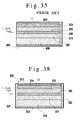
- Fig.35 is a sectional view of a prior laser diode chip.
- Fig.36 is a schematic view of an example of an LD/PD module aligning a fiber, a ⁇ 1 laser diode and a ⁇ 2 photodiode on a straight line.
- Fig.37 is a schematic view of another example of an LD/PD module of the invention aligning a fiber, a lens, a ⁇ 1 laser diode and a ⁇ 2 photodiode on a straight line.
- Fig.38 is a section of the 1.3 ⁇ m laser employed in the present invention.
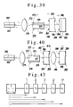
- Fig.39 is a schematic view of a third example of an LD/PD module of the invention aligning an optical fiber, a lens, a ⁇ 1 laser, a ⁇ 1 photodiode and a ⁇ 2 photodiode in series on a direct beam line.
- Fig.40 is a schematic view of a fourth example of an LD/PD module of the invention aligning an optical fiber, a lens, a ⁇ 1 laser, a ⁇ 1 photodiode, a lens and a ⁇ 2 photodiode in series on a direct beam line.
- Fig.41 is a horizontally-sectioned view of a sixth example of another LD/PD module containing a fiber, a lens, a ⁇ 1 laser, a ⁇ 1 PD and ⁇ 2 PD in series mounted on a submount in a box package.
- Fig.42 is a vertically-sectioned view of the same example.
- Fig.43 is an explanatory figure of the LD/PD module which aligns a laser LD1 emitting ⁇ 1 and eigen-wavelength photodiodes PD2, PD3, PD4, ⁇ , PDn sensing ⁇ 2, ⁇ 3, ⁇ , ⁇ n( ⁇ 1 ⁇ 2 ⁇ 3 ⁇ ⁇ ⁇ ⁇ n) in series in the order of raising the eigen wavelengths.
- Fig.10 demonstrates an example of a PD/LD module having a photodiode and a laser diode.
- the photodiode detects the ⁇ 1 light.
- the laser diode emits the ⁇ 2 light ( ⁇ 1 ⁇ ⁇ 2).
- An optical fiber (62) consists of a core (63) with a higher refractive index and a cladding with a lower refractive index enclosing the core.
- the light emitted from the fiber diverges in a cone with a top angle determined by the refractive indexes of the core and the cladding.
- the signal light ⁇ 1 goes into the photodiode (64) and is detected by the photodiode (64).
- the module Since the light ⁇ 1 diverges from the fiber (62), the module adopts a photodiode with a wide aperture.
- the light receiving surface has a diameter from 100 ⁇ m to 200 ⁇ m. A receiving surface of wider than a 100 ⁇ m diameter can catch almost all the light emitted out of the fiber (62).
- the photodiode (64) is not a conventional one but a special photodiode which has been first proposed by the present invention.
- the inner structure is simplified by depicting a substrate (65) and a reception layer (66).
- the substrate (65) includes the InP substrate and the InP buffer layer.
- the reception layer (66) contains the absorption layer and the window layer in the drawing.
- n-electrode (67) there is a ring p-electrode (67) on the periphery of the reception layer.
- An n-electrode (68) is formed on the periphery of the bottom of the substrate (65). The central part is not covered with the n-electrode (68). The central opening allows light to go out from the diode (64). In practice, all the entrance ⁇ 1 light has been absorbed by the reception layer (66) and does not attain the bottom opening.
- the photodiode of the present invention is characterized by selecting the band gaps of the window layer and the absorption layer, forming an annular n-electrode on the bottom of the substrate and allowing the incident light of a longer wavelength than ⁇ z to pass the device from the top surface to the bottom surface or from the bottom surface to the top surface.
- the photodiode is named a "wavelength-selective photodiode(PD)" in short hereinafter.
- the wavelength-selective photodiode (64) is followed by a laser diode chip (70) which emits the ⁇ 2 light.
- the light emanates from an end of the chip (70).
- the end is vertical to the beam line. Namely, the beam line is parallel to the surface of the laser (70).
- the semiconductor laser diode (70) has been produced by the steps of growing epitaxially an active layer (72) and a contact layer (73) on a substrate (71), attaching a stripe p-electrode (75) on the top of the contact layer (73), forming an n-electrode (74) on the bottom of the substrate (71). In the case of a buried type laser, burying layers sandwich the central active layer (72).
- the active layer (72) has a double-hetero structure. Injection of a current from the p-electrode to the n-electrode oscillates the laser (70) to emit the ⁇ 2 light.
- the laser (70) is, however, a conventional laser. There is no need of explaining the detailed structure.
- the light ⁇ 2 2 carrying a signal from the laser (70) goes into the photodiode (64) from the bottom, passes the diode without loss and goes out from the top surface. Then, the ⁇ 2 light enters the fiber (62) and travels in the fiber as a transmission signal.
- the present invention makes a special photodiode which detects ⁇ 1 but does not sense ⁇ 2.
- the photodiode is constructed with an InGaAsP window layer ( ⁇ w) and an InGaAsP absorption layer ( ⁇ z) for satisfying the requirement of ⁇ w ⁇ ⁇ 1 ⁇ ⁇ z ⁇ ⁇ 2.
- the ratio of the components of the window layer is determined by the conditions of ⁇ w ⁇ 1.3 ⁇ m and the lattice-fitting.
- the ratio of the components of the absorption layer is determined by the conditions of 1.3 ⁇ m ⁇ ⁇ z ⁇ 1.5 ⁇ m and the lattice-fitting. Restriction of the range of sensitivity of the photodiode (64) permits the laser light to pass the PD (64) without loss.
- Fig.11 shows example 2 which raises the efficiency of introducing the laser light ⁇ 2 into the core (63) of the fiber (62) by interposing a lens (77) between the fiber (62) and the wavelength-selective photodiode (64). Other parts and disposition are similar to example 1.
- the light beams ⁇ 1 launched from the fiber core (63) are converged by the lens (77) to the wavelength-selective PD (64), are fully absorbed by the reception layer (66) and are converted to a photocurrent.
- the laser (70) generates the light ⁇ 2 longer than ⁇ 1 ( ⁇ 2 > ⁇ 1).
- the light ⁇ 2 comes into the PD (64) from the bottom, penetrates the PD (64) and goes out of the PD(64).
- the ⁇ 2 beams are converged by the lens (77). Almost all of the beams are admitted to enter the core (63) of the fiber (62).
- the lens (77) heightens the connection between the fiber (62) and the laser (70).
- the power from the fiber (62) to the PD (64) is also strengthened by the lens (77).
- Fig.12 shows another example which exchanges the positions of the lens and the PD (64) in Fig.11.
- a lens (78) is interposed between the PD (64) and the laser (70).
- the lens (78) is assigned to converge the light ⁇ 2 of the laser (70) on the core (63) of the fiber (62).
- the light ⁇ 2 is converged by the lens (78) and penetrates the wavelength-selective photodiode (64) from the bottom to the top.
- the selection of the front lens type of Fig.11 or the rear lens type of Fig.12 should be contingent on the desired coupling efficiency, the photodiode, the laser diode, the mount of the lens and the shape and size of the package.
- Fig.13 exhibits a fourth example which adds another photodiode (85) behind the laser (70) for monitoring the power of the laser (70).
- the photodiode (85) is an ordinary one having a substrate (86) and a light reception layer (87) grown on the substrate (86).
- the reception layer means a set of a buffer layer, an absorption layer, a window layer and a p-region.
- a ring p-electrode (88) is formed on the p-region.
- An n-electrode (89) covers the whole bottom of the substrate (86).
- the photodiode (85) for monitoring has no opening on the bottom.
- the preceding photodiode (64) is the wavelength-selective one according to the idea of this invention.
- the light ⁇ 1 from the fiber (62) is detected by the photodiode (64).
- the laser (70) emits ⁇ 2 light beams both in the forward direction and in the rear direction.
- the forward ⁇ 2 beams are converged by a lens (79), pass the PD (64) and go into the fiber (62) with high efficiency.
- the rear ⁇ 2 beams reach the rear PD (85) which detects the power by the photocurrent.
- the oscillation of the laser (70) is stabilized by maintaining the photocurrent of the PD (85) at a constant level.
- a change of temperature varies the emission performance of a laser.
- the monitoring photodiode (85) enables the module to drive the laser (70) with a constant power in spite of the fluctuation of temperature.
- Two lenses (80) and (81) are provided for converging light beams.
- the forward lens (80) intervenes between the fiber (62) and the wavelength-selective photodiode (64).
- the rear lens (81) is interposed between the PD (64) and the laser (70).
- the lens (80) has a forward focus just at the end of the fiber (62).
- the beams from the fiber (63) become parallel beams by the lens (81).
- the back focus of the other lens (81) coincides with the end of the laser (70).
- the lens (81) converts the diverging beams of the laser (70) to parallel beams.
- the laser light passes the PD (64) as parallel beams and converges on the fiber end by the lens (80).
- Parallelism of ⁇ 1 and ⁇ 2 beams enables example 5 to determine freely the positions of the fiber (62), the PD (64) and the laser (70) on the beam line.
- Fig.15 denotes another example including a photodiode having a built-in lens (82) on the bottom of the substrate (65).
- the lens protrusion can be produced by etching stepwise the part of the substrate (65).
- the built-in lens (82) converges the light ⁇ 2 to the fiber (62).
- Another example is give by eliminating the lens (81) from the example of Fig.14 or replacing the PD (64) and lens (79) in Fig.13.
- the module aligns the fiber end, the lens, the PD (64), the laser (70) and the PD (85). A detailed embodiment will be explained by Fig.19 later.
- the point of the present invention is an improvement of a photodiode.
- the photodiode for the optical communication using 1.3 ⁇ m and 1.55 ⁇ m is clarified by referring to Fig.16.
- the substrate (92) is an n-InP wafer.
- the epitaxial layers can be produced by the MBE (molecular beam epitaxy) method, the MOCVD (metalorganic chemical vapor deposition) method or the chloride VPE method.
- the conventional PD had a wide wavelength difference ( ⁇ z- ⁇ w) of 0 .75 ⁇ m between the window layer ⁇ w and the absorption layer ⁇ z.
- the wide gap gives the wide range of sensitivity of Fig.9.
- the gap ( ⁇ z- ⁇ w) 0.27 ⁇ m is very small. Namely the sensitivity is restricted in a narrow scope.
- the restricted range endows the photodiodes of the invention with the eigen wavelength property.
- the thicknesses of the layers are, for example, 350 ⁇ m for the n-InP substrate, 2.5 ⁇ m for the n-InP buffer layer, 5 ⁇ m for the InGaAsP light receiving layer and 1.5 ⁇ m for the InGaAsP window layer.
- the suitable thickness of the window layer is 1 ⁇ m to 4 ⁇ m and the proper thickness of the receiving layer is 1 ⁇ m to 7 ⁇ m.
- Fig.17 shows the result of measurement of the relation between the transparency (relative ratio) and the wavelength ( ⁇ m) of the epitaxial wafer.
- the abscissa is the wavelength ( ⁇ m).
- the ordinate is the relative transparency (%).
- the light having the wavelength longer than 1.51 ⁇ m fully passes through the epitaxial wafer.
- the light with the wavelength shorter than 1.33 ⁇ m is entirely absorbed by the epitaxial wafer.
- the transparency rapidly changes from 0% to 100% in a narrow scope of wavelength of 0.18 ⁇ m in the epitaxial wafer basing the present invention.
- P-regions (96) are produced by masking the wafer and diffusing p-dopant into the epitaxial wafer through the openings of the mask.
- P-electrodes (97) are formed in a ring-shape on the p-regions (96).
- the top surfaces of the p-regions (96) enclosed by the p-electrodes (97) are covered with transparent antireflection films (98).
- the extra surfaces outside of the p-electrodes (97) are protected with passivation films (99).
- Annular n-electrodes (101) are formed on the bottom of the substrate in ohmic contact with the n-InP substrate.
- the central parts are openings for allowing light to pass through.
- Antireflection films (102) e.g., SiON films are formed on the openings.
- the wafer is cut crosswise and lengthwise along cleavage lines into individual chips. Chips are mounted on suitable packages for producing photodiodes.
- Light can enter the chip both from the bottom opening and from the top opening of (100) the device.
- the light going into the chip from the top opening (100) is reception light.
- the light going into the device from the bottom opening is transmission light.
- the antireflection films (98) and (102) suppress the incident light from reflecting on the surfaces for prohibiting the reflecting light from disturbing the oscillation action of the lasers.
- the photodiode of the present invention is characterized by the selection of the edge wavelengths ⁇ w and ⁇ z of the window layer and the absorption layer and the bottom opening enclosed by the n-electrode.
- Fig.18 denotes the sensitivity dependence upon the wavelength of the photodiode.
- Photocurrents have been measured at a reverse bias of 5V.
- the sensitivity is defined as a quotient of the photocurrent (A) divided by the light power (W).
- the sensitivity curve consists of a rising part (S), a high-sensitivity plateau (T) and a falling part (U).
- the sensitivity range (T) of the PD of the present invention is far narrower than the corresponding range (Q) of the conventional PDs in Fig.9.
- the end of the falling part (U) is about 1.42 ⁇ m.
- the light of a wavelength longer than 1.42 ⁇ m cannot be detected, because the absorption layer does not absorb the light.
- the sensitivity scope has only a 0.27 ⁇ m width ranging from 1.15 ⁇ m to 1.42 ⁇ m.
- the sensitivity scope includes 1.3 ⁇ m but excludes 1.55 ⁇ m.
- the photodiode is highly sensitive to 1.3 ⁇ m but is fully insensitive to 1.55 ⁇ m. The photodiode can deduce only the 1.3 ⁇ m light from a mixture of 1.3 ⁇ m light and 1.55 ⁇ m light. Thus, this is an eigen wavelength photodiode for 1.3 ⁇ m.
- the module contains a header (111), an eigen-wavelength photodiode (64), a laser chip (70) and another photodiode (85).
- the metallic header (111) is made e.g., from covar, iron or copper-tungsten.
- the embodiment employs a cover header which is provided with four lead pins (112), (113), (114) and (115) projecting downward from the bottom.
- the ground pin (112) is directly welded on the header (111).
- the other pins pierce through holes into the inner space.
- the pins are glued to the holes by an adhesive.
- a submount (120) is soldered on the top of a pole (119) projected from the header (111).
- the submount is a plate of an insulator metallized on both surfaces.
- the submount is, for example, an alumina (Al 2 O 3 ) plate.
- Suitable solder is AuSn, AuGe or SnPb.
- the submount (120) is soldered with AuSn in the embodiment.
- An eigen-wavelength photodiode (64) is fixed by the AuSn solder on the submount (120) in the surface orientation of being perpendicular to the beam line.
- a wire (121) connects the electrode of the PD chip (64) to the lead pin (114).
- the submount (120) has a notch (128) or hole (132).
- the PD chip (64) is positioned at a point just above the notch (128) or the hole (132).
- Another insulating submount (122) is fixed by solder on a vertical plane of the pole (119).
- the submount (122) is made from e.g., aluminum nitride (AlN). Both surfaces are coated with metal by printing.
- the submount (122) is parallel with the beam line.
- a laser chip (70) is bonded on the submount (122).
- the beam line of the laser coincides with the beam line of the fiber (62).
- a submount (123) is soldered on the slanting part.
- a monitoring photodiode (85) is soldered on the submount (123). The photodiode is not vertical to the beam line for suppressing the reflected light from returning to the laser (70).
- Fig.20 shows examples of submount for the PD (64).
- Fig.20(A) denotes a submount (120) having a rectangular notch (128) for admitting light to pass. All the other surfaces (top surface, bottom surface and sides) are coated with metal thin films (130). The bottom n-electrode is bonded on the top metallized surface. The bottom metallized surface is bonded on the pole (119). Thus, the n-electrode is electrically connected to the header (111), which saves a step of wirebonding.
- the p-electrode of the PD (64) is joined to the lead pin (114) by a golden wire (121) of a 30 ⁇ m diameter.
- the diameter of the light reception aperture (100) of the PD (64) is 200 ⁇ m.
- the span of the notch (128) is 250 ⁇ m.
- the length of the notch is 500 ⁇ m which is equal to the size of the PD chip (64).
- the submount (120) of Fig.20(b) is partially metallized.
- the n-electrode is in contact with the partial metallized part (129).
- the metallized part (129) is joined to the pin (115) with a wire.
- the size of the rectangular notch (128) is 250 ⁇ m ⁇ 500 ⁇ m like the former example of Fig.20(a).
- the submount (120) of Fig.20(c) has a circular hole (132) instead of the notch.
- the whole surfaces are coated with metal films.
- All the submounts have a common thickness of 500 ⁇ m. In any cases, the submount is positioned by harmonizing the rear end of the submount with the back wall of the pole (119) without special adjustment.
- a cylindrical cap (124) with a lens is fixed on the header (119) by putting the cap (124) on the header (119), filling an inert gas (e.g. argon gas or nitrogen gas) into the cap and welding the cap (124) to the header (119) airtightly.
- the cap (124) requires a window.
- the window needs a glass plate or a glass lens.
- the embodiment uses a ball lens (126) for heightening the coupling efficiency by converging the beams emitted from the laser (70) on the end of the fiber (62).
- An important matter is an alignment of the laser (70), the lens (126) and the optical fiber (62).
- the alignment is carried out by injecting current to the laser (70), lightening the laser (70), guiding the light into the fiber (62) and monitoring the power at the other end of the fiber (62).
- the optimum positions of the lens (126) or the fiber (62) are searched by displacing the cap (124) or the fiber (62). Then, the parts are fixed at the positions where optimum power is obtained through the fiber (62).
- the PD (64) dose not need a rigorous alignment.
- the tolerance in the directions orthogonal to the beam line is generous owing to the wide aperture (100) of the light receiving region.
- the PD (64) does not require converging beams. Namely, there is no need of the PD (64) being settled at the image point of the fiber end with regard to the lens (126).
- this invention does not place the PD (64) at the image point of the fiber. This is a strange mode of detection. Since the photodiode detects the total power of the light, the output power is scarcely affected by the position of the PD along the beam line unlike the image processing device, e.g. a camera.
- the example has three semiconductor chips or five optical devices including the lens (126) and the fiber (62). If all the five parts had to be aligned in a beam line, the alignment would be very difficult and the yield would be reduced.
- the devices requiring the alignment are only the laser (70), the lens (126) and the fiber (62). Since the PD vanishes from the steps of adjustment, the alignment is quite similar to the well-known alignment of a laser module.
- the embodiment can be realized by improving a conventional LD module with a bit of contrivance. Additional steps are changing of the shape of the pole, mounting the PD chip and connecting the electrodes to leads with wires. Such a slight addition of the steps effectively simplifies the multiwavelength, bidirectional optical communication network.
- the output power is measured at the other end of the fiber when the 1.55 ⁇ m LD (70) is lightened.
- the output power is similar to the power of the device without the PD chip (64).
- the interposition of the PD (64) has no bad effect upon the coupling between the fiber (62) and the laser (70).
- the output from the fiber (62) is measured by the PD (64) when 1.3 ⁇ m light is introduced into the other end of the fiber (62).
- the output is similar to the PD module without the LD.
- the defocus of the PD does not affect the output of the PD (64), since the wide aperture allows the PD to absorb all the power at any position on the beam line.
- the exterpolation of the laser is not a bad influence upon the PD (64).
- the laser (70) and the photodiode (64) independently emits or detects their own light without correlation.
- Fig.21 shows another embodiment which couples the module of Fig.19 with a fiber.
- the module has coupled a fiber to the Fig.19 module by welding a ferrule having an end of a fiber to a header (111).
- the parts enclosed by the header (111) and a cap (124) are the same as embodiment 1.
- An eigen-wavelength photodiode (64) is fixed via a submount (120) on the top of a pole (119).
- a metallized part (129) is connected by a wire to a lead pin (115).
- a p-electrode is joined to a pin (114) by another wire.
- a laser (70) is mounted on a side of the pole (119). The beam line of the laser (70) is vertical to the header (111).
- Embodiment 2 includes a ferrule holder (133), a ferrule (136) and a bending limiter (134) in addition to the PD/LD module of embodiment 1.
- the ferrule (136) is a tubular member holding an end of the optical fiber (62) in the hole.
- the ferrule-holder (133) is a metallic cylinder having a conical top. A hole is pierced at the top of the ferrule-holder (133). The ferrule (136) is inserted and fixed in the hole. A bottom end (137) of the ferrule (136) is slantingly cut at an angle of 8 degrees for preventing reflected light from returning to the laser (70).
- the ferrule-holder (133) and the ferrule (136) are made from metal, for example, stainless steel.
- the bending limiter (134) is made from an elastic material, for example, rubber or plastics.
- the bending limiter (134) is capped on the ferrule-holder (133).
- the bending limiter (134) protects the fiber from curving in a small radius.
- the alignment of the laser (70), the photodiode (64) and the lens (126) has been carried out. Then, the fixation of the holder (133) and the ferrule (136) is explained.
- the laser diode is excited to emit light by supplying a current.
- the holder (133) is displaced in two dimensional directions on the surface A of the header (111), while the light power is watched at the other end of the fiber.
- the output power takes the maximum value
- the holder (133) is welded on the point by the YAG laser welding or the electric welding.
- the ferrule is axially displaced in the hole of the holder for seeking the point which gives a prescribed coupling ratio.
- the ferrule (136) is welded to the holder (133) by irradiating YAG laser beams to the point B.
- Fig.22 shows another embodiment which allows a fiber to attach to or detach from a receptacle.
- a unit PD/LD module is fixed to a connector. The connector is separable.
- a header (111) sustains a PD (64), an LD (70) and a PD (85) on the upper surface.
- a cylinder (140) is welded on the header (111). At the top of the cylinder (140), a dummy fiber holder (141) is fixed. The dummy fiber holder (141) holds a dummy fiber (142) with a slanting end. The slanting end prevents the reflected light from returning to the laser (70).
- the ends of the dummy fiber holder (141) and the cylinder (140) are welded on the bottom of a female housing (143) of the connector.
- the female housing (143) has a cylindrical part and a wide flange (145). Several screw holes (146) are perforated.
- a male screw part (147) is provided on the outer surface of the cylindrical part.
- a sleeve (148) with low friction is inserted into the hole of the cylindrical part.
- the sleeve (148) is made from e.g. zirconia.
- a male connector (150) has a cylindrical housing (151) for holding an end of an optical fiber cord (152).
- the housing (151) sustains a union nut (153) on the outer surface.
- the front part of the housing (151) maintains a ferrule (155) sustaining an optical fiber (154).
- the end of the fiber (154) is polished in a round surface.
- a hole (not shown) is perforated axially on the female housing (143) for coupling the key (156).
- the pair of the connectors are coupled together by inserting the male connector (150) into the female connector (143) and tightening the union nut (153) to the male screw part (147).
- the optical fiber (154) comes into contact with the rear end of the dummy fiber (142). Travelling in the optical fiber cord (152), the signal light attains at the lens (126) and the PD (64) and is absorbed by the PD (64). The signal light emanating from the laser (70) is converged by the lens (126) and is guided to the dummy fiber (142).
- the embodiment has an advantage of the freedom of attaching and detaching the fiber from the connector.
- the alignment has been carried out between the dummy fiber and the lens.
- the freedom enables the module to adapt itself to different fibers in common.
- the embodiment also aligns an eigen-wavelength photodiode (64), a laser diode (70) and a photodiode (85) for monitoring along a straight beam line.
- the LD/PD module mounts the devices in a covar package (160) and a covar cap (161) instead of the cylindrical package of Fig.19, 21 or 22.
- the package (160) contains an AlN submount (162) on which the optoelectronic devices are fixed.
- the submount (162) is provided with the eigen-wavelength photodiode (64) for selecting exclusively 1.3 ⁇ m at the front (163).
- a triangle notch (164) is bored at a point following the PD (64) on the submount (162).
- the submount (162) has a flat part (165) and a protrusion (166) at the rear end.
- the monitoring photodiode (85) is affixed via a metal coating (167) to the end protrusion (166).
- Another submount (168) is fixed on the flat part (165).
- a 1.55 ⁇ m emitting laser diode (70) is bonded on the submount (168).
- a lens (170) is mounted on the notch (164).
- the wavelength-selective photodiode (64) is installed via a submount (169) on the front end of the larger submount (162).
- the eigen-wavelength photodiode (64) only senses 1.3 ⁇ m but allows 1.55 ⁇ m to pass thought it.
- the package (160) has six pins (171), (172), (173), (174), (175) and (176) at the bottom which are insulated from the package (160).
- An axial hole (177) is bored at the forefront of the package (160).
- An optical fiber cord (178) is inserted in the hole (177).
- the front end of the fiber (179) faces with the eigen-wavelength photodiode (64).
- the end (180) of the fiber is ground and polished slantingly for preventing the reflected light from returning to the laser (70).
- the notch, the protrusion and the step facilitate positioning of the optoelectronic devices on the submount (162).
- the upper surface of the submount (162) is provided with metal coatings (181), (182), (183), (184), (185) and (186) for wiring patterns.
- the n-electrode of the wavelength-selective photodiode (64) is soldered to the metallized pattern (186).
- the metallized pattern (186) is connected to the lead pin (176) with a wire (196).
- the p-electrode of the PD (64) is coupled to a metallized pattern (181) with another wire (191) to the pin (171).
- the LD (70) is soldered on the metallized pattern (185) which is coupled by a wire (195) to the pin (175).
- Another electrode of the LD (70) is connected to the metallized pattern (182) by a wire (197).
- the pattern (182) is led to the pin (172) by a wire (192).
- the monitoring photodiode (85) is fixed upon the metallizing (184) with a solder.
- the metallized (184) is coupled to the pin (174) by a wire (194).
- the other electrode of the PD (85) is coupled via a wire (198), the metallized coat (183) and a wire (193) to the pin (173).
- the submount is soldered on the package, after all the optoelectronic devices have been mounted on the submount and the lens has been fixed on the notch. Then, the electrodes, the metallized coats and the pins are connected by wirebonding.
- Positioning of the fiber is carried out by loosening the fiber with regard to the package, driving the LD (70) to emanate, measuring the output at the other end of the fiber and fixing the fiber in the hole (177) with an epoxy resin, when the output attains to the predetermined power. Then, the package (160) is covered with the cap (161) and sealed airtight by the seam-seal method in dry nitrogen atmosphere.
- the LD/PD module is examined by introducing 1.3 ⁇ m light into the fiber, lightening the 1.55 ⁇ m laser and detecting the 1.3 ⁇ m light by the wavelength-selective photodiode (64).
- the examination confirmed that the PD (64) exhibits the same sensitivity as an isolated 1.3 ⁇ m photodiode and confirmed that the PD and the LD operate individually at the eigen wavelengths.
- a 1.3 ⁇ m wavelength-selective photodiode (200) is installed face to face with an optical fiber (62).
- the eigen-wavelength photodiode (200) has an opening on the rear surface.
- the edge wavelength ⁇ w1 of the window layer and the edge wavelength ⁇ z1 of the absorption layer satisfy an inequality of ⁇ w1 ⁇ 1.3 ⁇ m ⁇ ⁇ z1.
- the difference ( ⁇ z1- ⁇ w1) is small enough.
- a 1.46 ⁇ m eigen-wavelength photodiode (201) lies at a point following the 1.3 ⁇ m PD (200).
- the 1.46 ⁇ m PD (201) has the similar properties of having an opening on the back and a small difference ( ⁇ z2- ⁇ w2) and of satisfying an inequality of ⁇ w2 ⁇ 1.46 ⁇ m ⁇ z2.
- a 1.55 ⁇ m laser (70) is provided at an end of the beam line for producing transmission signals.
- the laser light of 1.55 ⁇ m passes through the 1.46 ⁇ m PD (201) and the 1.3 ⁇ m PD (200) and goes into the optical fiber (62).
- the transmission signals are carried by the 1.55 ⁇ m light in the optical fiber from the module to the station.
- the photodiodes explained hitherto are the vertical-type photodiodes which have an annular p-electrode and a ring n-electrode for allowing light to pass the diode in the vertical direction. Otherwise, this invention can be utilized to a special, horizontal type photodiode (210) which is shown by Fig.26.
- P-regions (215) are produced at the center of chips by diffusing zinc as a p-impurity. Instead of an annular electrode, a wide, planar p-electrode (216) is evaporated on the p-region (215). The whole bottom of the n-InP substrate is covered with an n-electrode (217). Signal light is introduced in a horizontal direction to a side of the InGaAsP light receiving layer (213). Such a horizontal photodiode (210) is also feasible to the present invention.
- Fig.27 shows another PD/LD module constructed with a horizontal photodiode (210) and a laser (70) which are aligned in a beam line.
- the signals are sent from the broadcasting station by the light of 1.3 ⁇ m to the ONU modules.
- the signal light is fully absorbed by the first PD (210).
- the semiconductor laser (70) emits the 1.55 ⁇ m light for transmitting signals from the ONU to the central station.
- the 1.55 ⁇ m light pass the PD (210) without loss.
- the PD/LD module of the present invention can be built also with the horizontal photodiodes.
- the module consisting of n horizontal eigen-wavelength photodiodes ( ⁇ 1 ⁇ 2 ⁇ 3 ⁇ n) has the following advantages over a module of the vertical photodiodes.
- AlGaAs mixture crystals satisfy the lattice-fitting condition with GaAs crystal in a wide range of the mixture ratio. All AlGaAs crystals have narrower band gaps than GaAs. If an AlGaAs photodiode having a GaAs substrate and an AlGaAs absorption layer is made, the light dispersed out of the AlGaAs absorption layer will safely be absorbed by the substrate, the buffer layer or the window layer due to the narrower band gaps. Such an AlGaAs photodiode will be endowed with the wavelength selectivity suitable for horizontal reception from the structural feature. Of course such a photodiode has never been produced, since there is no need for the AlGaAs photodiodes. The current technology can make such AlGaAs PDs, if necessary.
- FIG.36 A basic embodiment is demonstrated by Fig.36.
- the inner structure is omitted in the figure for simplifying the explanation.
- the embodiment has a ⁇ 1 laser diode (270) facing with the end of a fiber (262) and a ⁇ 2 photodiode (285) following the laser (270).
- the ONU terminals send signals by the ⁇ 1 light to the central station.
- the station sends signals riding on the ⁇ 2 light to the ONUs.
- ⁇ 2 is called “reception light”
- ⁇ 1 is called “transmission light”.
- the ⁇ 2 light from the station is received by the ONU terminals and detected by the PD (285).
- the laser (270) has an InP substrate, an InP cladding layer, an active layer (272) and an InP cladding layer (273) which have been grown epitaxially on the substrate.
- a p-electrode (275) is formed on the upper surface and an n-electrode (274) is formed on the bottom of the substrate.
- the active layer is transparent to the ⁇ 2 light.
- the ⁇ 2 reception light passes the laser (270) without loss.
- a photodiode (285) for receiving ⁇ 2 is furnished at the back of the laser (270).
- the photodiode (285) has an InP substrate, an InP buffer layer, an InGaAs light receiving layer, an InP window layer, an annular p-electrode (288) and an annular n-electrode (289).
- (286) denotes both the substrate and the buffer layer.
- (287) indicates both the window layer and the light receiving layer.
- the inner structure is omitted for simplicity.
- the rear side of the laser is coated with a reflection layer for reflecting the ⁇ 1 light completely but allowing the ⁇ 2 to pass through. Thus, only the ⁇ 2 light reaches the photodiode (285) and is detected by the PD in Fig.36.
- the inequality ⁇ 1 ⁇ ⁇ 2 enables the embodiment to realized such relation.
- ⁇ 1 and ⁇ 2 are assigned to be 1.3 ⁇ m and 1.55 ⁇ m respectively.
- the laser has an InP substrate and an InGaAsP active layer.
- the absorption edge of the active layer is 1.3 ⁇ m.
- 1.55 ⁇ m light can pass the active layer, if 1.55 ⁇ m light is directed to the layer.
- the 1.3 ⁇ m laser can be a window for the 1.55 ⁇ m light, because the laser does not absorb 1.55 ⁇ m light.
- the InGaAsP active layer plays the role of a waveguide for 1.3 ⁇ m light, which encloses and restricts the object light beams. Going into the laser at the front, the 1.55 ⁇ m light travels in the active layer and goes out of the rear end of the layer.
- the photodiode however, has a sufficiently wide light receiving region of about 100 ⁇ m to 200 ⁇ m diameter. Then, nearly all the beams are received by the aperture of the photodiode (285).
- This invention succeeds in making an LD/PD module of sending signals by 1.3 ⁇ m light and of receiving signals by 1.55 ⁇ m light by aligning a 1.3 ⁇ m LD and a 1.55 ⁇ m PD in series without WDMs.
- the module requires a contrivance of preventing the 1.3 ⁇ m laser light from going back to the photodiode, since the photodiode has some sensitivity to 1.3 ⁇ m.
- the rear end of the laser is coated with a reflection film which is reflective to 1.3 ⁇ m light but transparent to 1.55 ⁇ m light.
- This invention demands a 100% reflection mirror for 1.3 ⁇ m.
- the selective mirror can be produced by piling a plurality of several kinds of dielectric films with different refractive indices and thicknesses.
- Embodiment 7 is a basic module of the PD+LD type of the present invention. There are also some versions of this type of PD+LD for enhancing the performance of bidirectional multiwavelength optical communication network.
- Fig. 37 shows another embodiment having a lens, a laser and a photodiode.
- a lens (277) is interposed between an optical fiber (262) and a laser (270) for enhancing the efficiency by converging the 1.3 ⁇ m laser light to the fiber (263).
- the lens (277) converges also the 1.55 ⁇ m light from the fiber (263) to the active layer of the laser (270) for penetrating the laser with a high efficiency.
- the lens raises the sensitivity for reception light and the power of the transmission light.
- An additional photodiode often accompanies a laser for regulating the power by monitoring the output power of the laser (Fig.39).
- a photodiode is furnished behind the laser in this module.
- the module controls the output of the laser by monitoring the light emitted backward from the laser, changing the driving current in the direction for reducing the difference between the actual power and the preferable power.
- the feed-back control is well know for driving laser modules.
- a monitoring photodiode were positioned behind the laser, the monitoring photodiode would annihilate the reception signals in front of the main photodiode.
- a conventional photodiode annihilates both ⁇ 1 + ⁇ 2 by the wide bottom n-electrode (61), when the monitoring photodiode were shot by ⁇ 1 + ⁇ 2.
- a conventional photodiode cannot be employed as a monitoring photodiode in the module of the present invention, even if the shape of the n-electrode were changed into an annular one.
- a photodiode has already been given just by the present invention by Fig.16.
- the PD in the former PD + LD type modules can directly be adopted as a monitoring photodiode, because the new PD can let light of longer wavelengths pass through.
- An LD/PD module of Fig.39 is produced by assembling the beforementioned laser, the narrow range monitoring photodiode and the final 1.55 ⁇ m photodiode in series.
- an end of a fiber (262), a lens (278), a 1.3 ⁇ m laser chip (270), a 1.3 ⁇ m eigen-wavelength photodiode (264) and a 1.55 ⁇ m photodiode (285) are aligned on a straight line.
- the laser (270) emits 1.3 ⁇ m light signals in both directions.
- the backward light is detected by the monitoring wavelength-selective photodiode (264) for regulating the power.
- the forward light is converged by the lens (278) and is introduced into the fiber (262) for carrying the signals from the terminal to the central station.
- the 1.55 ⁇ m light spreading out of the fiber (262) passes the lens (278), the laser (270) and the PD (264) without attenuation and arrives at the end 1.55 ⁇ m PD (285).
- the 1.55 ⁇ m PD converts the light signals from the central station into electric ones.
- Fig.40 shows another embodiment having an additional lens (280) between the monitoring ⁇ 1 PD (264) and the end ⁇ 2 PD (285) to the previous example of Fig.39.
- the lens (280) enables the ⁇ 2 PD (285) to receive the ⁇ 2 (1.55 ⁇ m) signal light with sufficient efficiency over a considerable distance.
- the lens enhances the freedom of design of the devices.
- a conventional laser diode has reflection films on both ends for making a resonator which reciprocates light between the end reflection films for absorbing pumping energy sufficient to emit coherent light.
- the rear end film has a higher reflection rate than the front film, since the light emitted from the front is used for various objects.
- the backward light is used for regulating the power by monitoring the power by the inherent PD.
- the module would be inoperative, since the front and end mirrors would reflect the 1.55 ⁇ m light carrying the reception signals.
- Conventional reflection films have so small wavelength dependence that the films reflect almost all of the wavelengths near the emission wavelength. Little wavelength dependence has been deemed an ideal property of a mirror in general. If a 1.3 ⁇ m emission laser were to be employed in the linear LD/PD module, the end 1.55 ⁇ m PD cannot receive sufficient light power of 1.55 ⁇ m due to a big loss caused by the mirrors.
- the high speed, long range optical communication system requires to reduce the optical loss as small as possible. Furthermore, the Inventors have noticed that the refection of 1.3 ⁇ m does not inherently contradict the transit of 1.55 ⁇ m. The difficulty shall be solved by forming a selective mirror on the ends which reflects 1.3 ⁇ m but admits 1.55 ⁇ m. Namely, the Inventors have noticed to adopt a film which acts as a reflection film to 1.3 ⁇ m but an antireflection film to 1.55 ⁇ m. The problem is whether such a miracle film can be produced actually. The Inventors have found a way of producing such a wavelength-selective film by designing the thickness, refractive indexes of dielectric multilayers of the film (Fig.38).
- Such a dielectric multifilm can be made by the current evaporation methods or the current CVD methods.
- the film (321) which shall coat the front end of the laser is built by piling a 606 nm SiO 2 film, a 24nm a-Si(amorphous silicon) film and a 217nm SiO 2 film in the order near the chip end.
- the multifilm can be produced by the plasma CVD method.
- the dielectric film exhibits a 30 % reflection rate for 1.3 ⁇ m but has a 0.5% reflection for 1.55 ⁇ m.
- the selectivity for 1.3 ⁇ m and 1.55 ⁇ m is sufficient for making the module of the present invention.
- the other film (320) of Fig.38 which shall coat the rear end of the laser is produced by piling a 220 nm SiO 2 film, a 56nm a-Si film, a 103nm SiO 2 film, an 84nm a-Si film and a 470nm SiO 2 film in the order from the end by the plasma CVD method.
- the rear end film shows an 80 % reflection for 1.3 ⁇ m but 0.5% reflection for 1.55 ⁇ m.
- These films are suitable for the end coating of the laser of this invention.
- the films can be made from various assemblies of materials of refractive indexes and thicknesses besides the example. The adoption of these dielectric multilayers on the ends of the laser realizes the novel module of the present invention with stable transmission performance and high sensitive reception.
- Fig.38 shows the vertical section of the laser having such selective-films on both ends.
- the laser has been produced from an epitaxial wafer containing an n-InP substrate (318), an n-InP cladding layer (317), an InGaAsP active layer (316), an InP cladding layer (315) and an n-InGaAsP capping layer (314).
- P-regions are produced in stripes at the middle of chips by diffusing a p-impurity through a mask.
- the InGaAsP capping layer (314), the InP cladding layer (315) and the InGaAsP active layer (316) are partially converted from n-type to p-type conduction.
- Buried layers are grown on both sides of the active layer (316) for restricting the current and the light in narrow paths.
- the laser has a half-reflection film (320) coated on an rear end which fully reflects 1.3 ⁇ m light but admits 1.55 ⁇ m to pass.
- Another half-reflection film (321) coats a front end of the laser for reflecting 1.3 ⁇ m partially but admitting 1.55 ⁇ m.
- the laser allows 1.55 ⁇ m to pass through without loss.
- the passing 1.55 ⁇ m light has no influence on the laser, because, 1.55 ⁇ m light has smaller energy than the band gap of the active layer of the laser.
- Fig.41 and Fig.42 demonstrate an embodiment which contains optoelectronic devices in a box package.
- a covar box package maintains the 1.3 ⁇ m laser chip (325) of Fig.16 and the 1.3 ⁇ m wavelength-selective monitoring photodiode (264) and a 1.55 ⁇ m photodiode (285) for detecting the reception signals.
- a package (326) and a cap (327) are made from covar.
- a submount (328), an insulating plate, is fixed in the package (326). Notches or steps are formed on the submount. The submount is partially coated with metal films.
- a plurality of pins (331), (332) ⁇ project from the bottom of the covar package (326).
- a lens (330) is fitted in a notch (364) at the forefront of the submount (328).
- a laser chip (325) is fixed on a metal coating at a point behind the lens (330).
- a 1.3 ⁇ m selective photodiode (264) is mounted on a metal coat of the submount (328) for monitoring the output power of the laser (325).
- An end photodiode (285) is fixed on a metal coating (367) of the submount (328) behind the laser (325).
- An end of an optical fiber (338) is fixed in a hole (337) of the package (326). Traveling in the optical fiber (338), the 1.55 ⁇ m signals from the broadcasting station are converged by the lens (330), are led in the active layer of the laser (325) and the monitoring photodiode (264) and are detected by the end 1.55 ⁇ m photodiode (285).
- the 1.3 ⁇ m light emitted from the laser (325) is converged by the lens (330) to the optical fiber and is guided to the central station by the optical fiber (338). The power of the laser (325) is measured by the monitoring photodiode (264).
- the embodiment employs the 1.3 ⁇ m LD chip (325) of a size of 300 ⁇ m ⁇ 400 ⁇ m, the 1.3 ⁇ m PD (264) of 500 ⁇ m ⁇ 500 ⁇ m and the 1.55 ⁇ m PD (285) of 500 ⁇ m ⁇ 500 ⁇ m.
- the aperture of the 1.3 ⁇ m PD (264) is 300 ⁇ m in diameter.
- the aperture of the 1.55 ⁇ m PD (285) has a 200 ⁇ m diameter.
- the submount (328) is made from aluminum nitride (AlN). The submount is provide with the notch for the lens (330), the metal coatings and the grooves for mounting the LD (325), the PD (264) and the PD (285).
- the aperture of the preceding 1.3 ⁇ m PD (264) is designed to be larger than the aperture of the 1.55 ⁇ m PD (285) for preventing the 1.3 ⁇ m PD (264) from attenuating the 1.55
- the LD chip (325), the PD chip (264) and the PD chip (285) are soldered on the submount (328), for example, AuSn solder or SnPb solder.
- the lens (330) is glued to the submount by epoxy resin.
- the submount (328) is fixed on the package (326) by a solder.
- the electrodes and the metal coatings or metal coatings and lead pins are connected by wirebonding golden wires of a 30 ⁇ m diameter.
- the position of the fiber is adjusted by the steps of loosening the fiber (338) to the hole (337), exciting the laser (325), observing the power of 1.3 ⁇ m light at another end of the fiber (338), displacing the fiber for seeking the optimum position and adhering the fiber at the optimum position to the hole. Then, the package is sealed by the cap in dry nitrogen atmosphere, for example, by the seamseal method.
- the embodiment succeeds in enabling the 1.55 ⁇ m light to pass the 1.3 ⁇ m LD (325) and the 1.3 ⁇ m PD (264) and reach the 1.55 ⁇ m PD (285) at the end by aligning the LD (325), the PD (264) and the PD (285) on an extension of the beam line of the fiber (338).
- the module is examined by the test of exciting the 1.3 ⁇ m laser (325) and measuring the coupling efficiency between the module and the fiber.
- the power introduced in the fiber is as strong as the case of the laser without the front film (321) and the rear film (320).
- Another test of detecting the 1.55 ⁇ m light from the fiber by the PD (285) exhibits the similar sensitivity to the case of omitting the 1.3 ⁇ m LD (325) and 1.3 ⁇ m PD (264).
- the advantages of the embodiment are feasible mounting the module on a print plate owing to the rectangular shape of the box package.
- the use of the wide submount enables the embodiment to store a driving circuit of the laser, an amplifier of the PD or a signal processing circuit in the package.
- the PDs and the LD work independently.
- the PD/LD module of the invention exhibits higher performance than prior PD module or prior LD module which are connected by WDMs.
- the scope of the invention is not restricted to the embodiments. Variations are allowable with regard to the packages, lenses and caps of modules.
- the set of two wavelengths is not confined to the set of 1.3 ⁇ m/1.55 ⁇ m.
- the modules can be applied to any set of wavelengths.
- Favorable candidates are 1.46 ⁇ m/1.55 ⁇ m and 0.9 ⁇ m/1.3 ⁇ m in the lowest case of two wavelengths.
- the module according to the present invention can be produced by narrowing the sensitivity range of PDs and the emission range of an LD or LEDs in order not to overlap the emission region of ⁇ 1 and the sensitivity range of ⁇ 2.
- the LD/PD module is assembled by aligning a plurality of eigen-wavelength photodiodes PD1, PD2, PD3, ⁇ , PDn having eigen wavelengths of ⁇ 1, ⁇ 2, ⁇ 3, ⁇ , ⁇ n ( ⁇ 1 ⁇ 2 ⁇ 3 ⁇ n) in series in the order of increasing the eigen wavelengths and by aligning one or a plurality of light emitting devices following the series of the PDs.
- This invention constructs a linear module having only a linear beam line.
- this invention dispenses with expensive, bulky WDMs which bisect a path into two paths or unify two paths to one. Besides the WDMs, this invention excludes expensive dielectric multilayer filters which annihilate unnecessary light from the modules.
- n 2 (LD+PD)
- the prior module required three independent parts of a WDM (21), an LD module (25) and a PD module (27).
- the module of this invention consists only of one PD/LD module.
- Fig.28 shows the structure of the present invention corresponding to the prior one shown in Fig.5.
- An optical fiber (16) is connected to the LD/PD module (220) explained before via an optical connector (17).
- the photodiodes and the light emitting devices are all endowed with monochromaticity and are aligned in series in the order of raising wavelengths ( ⁇ 1 ( ⁇ 2( ⁇ 3 ⁇ n). All the PDs, the LEDs or the LD act independently without being disturbed by other devices. Thus, the module exhibits more superb a function than a sum of sole PD modules and sole LED modules.
- the scope of the protection is not restricted by the embodiments mentioned. Variations are available for the shape of packages, the existence of lenses, the kind of lenses or the connection with caps.
- the embodiments used two wavelengths of 1.3 ⁇ m and 1.55 ⁇ m.
- This invention allows higher order multiwavelength PD/LD modules of the number n higher than 2 (n ⁇ 3).
- Monochromatic PDs, LDs or LEDs can be produced at any wavelengths besides 1.3 ⁇ m, 1.46 ⁇ m and 1.55 ⁇ m.
- the system will conveniently be constructed by the PD/LD module of this invention having more than three PDs, LDs or LEDs in future.
- the essence of the present invention is eigen-wavelength or wavelength-selective optoelectronic devices.
- LEDs or LDs light emitting devices
- Photodiodes lack the monochromatic property, since PDs having a wide, flat range of sensitivity have been desired so far.
- Narrow band photodiodes contradict the common sense of the art.
- This invention tries to make such narrow sensitivity photodiodes for making linear PD/LD modules excluding WDMs or couplers.
- Monochromaticity of individual devices allows the modules to select arbitrary wavelengths for various purposes, which endows the PD/LD modules with high degree of flexibility.
- the other LD+PDs type of this invention assembles a linear PD/LD module by placing a ⁇ 1 laser which is transparent to ⁇ 2 on the beam line near the end of a fiber and placing a ⁇ 2 photodiode at the back of the laser on the beam line.
- the signal light progresses on a straight line without being separated spatially.
- the module does without WDMs, since the light is not divided into separated paths. Only a single PD/LD module can function as superbly as a prior PD/LD module which is constructed by three parts, i.e., a WDM, an LD module and a PD module.
- Fig.28 shows an ONU module making use of the module of the invention.
- the new ONU module has neither WDMs nor bisecting paths. Exclusion of bisections reduces the size of the module, the number of parts and the number of processes for production. Omission of WDMs reduces the loss due to WDMs. This invention is further immune from the joint loss, since the module is free from joints.
- the linear LD/PD module can be applied to a system including n different wavelengths of ⁇ 1 ⁇ 2 ⁇ 3 ⁇ n (Fig.43).
- the module has a laser LD emitting ⁇ 1 and (n-1) photodiodes PD2, PD3, PD4, ⁇ , PDn for sensing eigen wavelengths ⁇ 2, ⁇ 3, ⁇ , ⁇ n.
- the laser LD and the photodiodes PD2, PD3, PD4, ⁇ , PDn are aligned in series on a straight line which is an extension of the fiber.
- the j-th wavelength of ⁇ 1+ ⁇ 2+ ⁇ 3+ ⁇ + ⁇ n of the reception signals is allowed to pass LD, PD1, PD2, ⁇ ,PDj-1 and is absorbed by PDj by narrowing the sensitivity range of all the PDs. Namely, the selectivity is given by narrowing the sensitivity region of PDs.
- the eigen wavelengths ⁇ 2, ⁇ 3, ⁇ , ⁇ n are the middle values in the narrow sensitivity ranges.
- This invention enables the j-th eigen PDj to sense only ⁇ j among the reception signals of ⁇ 1+ ⁇ 2+ ⁇ 3+ ⁇ + ⁇ n.
- Prior modules would require (n-1) WDMs for separating n different wavelengths, if the system adopted n wavelengths.
- a WDM cannot entirely separate n different wavelengths in the ratio of 1:(n-1). It would be hard to separate n different wavelengths by WDMs.
- This invention can solve the difficulties of cross-talk and imperfect separation by making the best use of the wavelength selection by the absorption edge wavelengths of semiconductors.
Landscapes
- Light Receiving Elements (AREA)
- Optical Couplings Of Light Guides (AREA)
- Optical Communication System (AREA)
Applications Claiming Priority (4)
| Application Number | Priority Date | Filing Date | Title |
|---|---|---|---|
| JP319705/95 | 1995-11-13 | ||
| JP31970595A JP3324373B2 (ja) | 1995-11-13 | 1995-11-13 | 光送受信モジュ−ル |
| JP01935096A JP3232998B2 (ja) | 1996-01-09 | 1996-01-09 | 光送受信モジュ−ル |
| JP19350/96 | 1996-01-09 |
Publications (2)
| Publication Number | Publication Date |
|---|---|
| EP0773591A2 true EP0773591A2 (de) | 1997-05-14 |
| EP0773591A3 EP0773591A3 (de) | 1998-09-16 |
Family
ID=26356183
Family Applications (1)
| Application Number | Title | Priority Date | Filing Date |
|---|---|---|---|
| EP96307962A Withdrawn EP0773591A3 (de) | 1995-11-13 | 1996-11-04 | Lichtemittierende und lichtdetektierende Vorrichtung |
Country Status (2)
| Country | Link |
|---|---|
| US (1) | US5787215A (de) |
| EP (1) | EP0773591A3 (de) |
Cited By (7)
| Publication number | Priority date | Publication date | Assignee | Title |
|---|---|---|---|---|
| EP0901170A1 (de) * | 1997-09-03 | 1999-03-10 | Sumitomo Electric Industries, Ltd. | Wellenlängenselektive Fotodiode und Modul mit deren Verwendung |
| EP0924776A3 (de) * | 1997-12-09 | 2000-03-22 | Sumitomo Electric Industries, Ltd. | Photodiode |
| US6043550A (en) * | 1997-09-03 | 2000-03-28 | Sumitomo Electric Industries, Ltd. | Photodiode and photodiode module |
| WO2003029868A1 (en) * | 2001-09-28 | 2003-04-10 | Sony Corporation | Optical transmitter/receiver |
| EP1195632A3 (de) * | 2000-10-06 | 2004-05-12 | The Furukawa Electric Co., Ltd. | Photodiodenzeilen- Vorrichtung, ein Photodiodenmodul, und eine Anordnung zum Verbinden des Photodiodenmoduls mit einem optischen Verbinder |
| US6844607B2 (en) | 2000-10-06 | 2005-01-18 | The Furukawa Electric Co., Ltd. | Photodiode array device, a photodiode module, and a structure for connecting the photodiode module and an optical connector |
| EP2474034A4 (de) * | 2009-08-31 | 2014-02-26 | Intevac Inc | Tragbare niedrigenergie- und niedriglichtkamera mit wellenlängenbegrenzung |
Families Citing this family (53)
| Publication number | Priority date | Publication date | Assignee | Title |
|---|---|---|---|---|
| JP3767156B2 (ja) * | 1998-02-23 | 2006-04-19 | 住友電気工業株式会社 | 光送受信モジュ−ル |
| JP3399832B2 (ja) * | 1998-04-20 | 2003-04-21 | シャープ株式会社 | 双方向光通信器および双方向光通信装置 |
| DE19834090A1 (de) * | 1998-07-29 | 2000-02-03 | Heidenhain Gmbh Dr Johannes | Optoelektronische Sende- und Empfangseinheit |
| US6456369B1 (en) * | 1999-01-29 | 2002-09-24 | Ando Electric Co., Ltd. | Multi-core optical fiber inspecting method and apparatus |
| JP2000241642A (ja) * | 1999-02-17 | 2000-09-08 | Sumitomo Electric Ind Ltd | 光送受信モジュール |
| US7212556B1 (en) * | 1999-02-17 | 2007-05-01 | Matsushita Electric Industrial Co., Ltd. | Semiconductor laser device optical disk apparatus and optical integrated unit |
| JP2001021775A (ja) * | 1999-07-09 | 2001-01-26 | Sumitomo Electric Ind Ltd | 光学装置 |
| KR100310088B1 (ko) * | 1999-07-31 | 2001-09-29 | 윤종용 | 파장분할다중화용 광소스의 파장 및 광출력 제어방법 |
| US6540412B2 (en) * | 2000-02-10 | 2003-04-01 | Sumitomo Electric Industries, Ltd. | Optical transceiver |
| US20030126075A1 (en) * | 2001-11-15 | 2003-07-03 | First Data Corporation | Online funds transfer method |
| US20030126036A1 (en) * | 2000-02-29 | 2003-07-03 | First Data Corporation | Online payments |
| US7366695B1 (en) * | 2000-02-29 | 2008-04-29 | First Data Corporation | Electronic purchase method and funds transfer system |
| JP3931545B2 (ja) * | 2000-03-22 | 2007-06-20 | 住友電気工業株式会社 | 発光モジュール |
| JP2001281501A (ja) * | 2000-03-30 | 2001-10-10 | Fujitsu Ltd | レーザダイオードモジュール及びその組立方法 |
| JP2001281506A (ja) * | 2000-03-31 | 2001-10-10 | Ngk Insulators Ltd | 光ヘッド |
| GB0013366D0 (en) * | 2000-06-01 | 2000-07-26 | Vipswitch Inc | Optical communicator |
| US6493475B1 (en) * | 2000-10-19 | 2002-12-10 | Tellium, Inc. | Monolithic integration of signal-monitoring scheme in an optical switch |
| DE10053670A1 (de) * | 2000-10-28 | 2002-05-08 | Daimler Chrysler Ag | Optisches Signalübertragungssystem |
| JP3921940B2 (ja) * | 2000-12-07 | 2007-05-30 | 住友電気工業株式会社 | 光送受信モジュール |
| US6782161B2 (en) * | 2001-02-05 | 2004-08-24 | Derma Laser Inc. | Laser diode apparatus provided with an aiming beam and injection method therefor |
| JP3788249B2 (ja) * | 2001-02-23 | 2006-06-21 | 住友電気工業株式会社 | 発光モジュール |
| US6793406B1 (en) * | 2001-03-12 | 2004-09-21 | Phillip J. Edwards | Light source monitoring apparatus |
| US6623180B2 (en) * | 2001-10-19 | 2003-09-23 | Gtran, Inc. | High frequency optical module and method of making same |
| DE10201102A1 (de) * | 2002-01-09 | 2003-07-24 | Infineon Technologies Ag | Laservorrichtung |
| JP3965997B2 (ja) * | 2002-01-15 | 2007-08-29 | 住友電気工業株式会社 | 光モジュール |
| JP3890999B2 (ja) * | 2002-02-14 | 2007-03-07 | 住友電気工業株式会社 | 光送信モジュール |
| TW561719B (en) * | 2002-05-31 | 2003-11-11 | Gigno Technology Co Ltd | Electric apparatus |
| US20030223131A1 (en) * | 2002-05-31 | 2003-12-04 | International Business Machines Corporation | Optical subassembly (OSA) having a multifunctional acrylate resin adhesive for optoelectronic modules, and method of making same |
| JP2004086136A (ja) * | 2002-07-01 | 2004-03-18 | Seiko Epson Corp | 光トランシーバの製造方法及び調整装置 |
| US20050141800A1 (en) * | 2002-09-17 | 2005-06-30 | Mitsubishi Denki Kabushiki Kaisha | Waveguide semiconductor optical device and process of fabricating the device |
| US7456945B2 (en) * | 2002-10-28 | 2008-11-25 | Finisar Corporation | Photonic device package with aligned lens cap |
| JP2004152991A (ja) * | 2002-10-30 | 2004-05-27 | Sumitomo Electric Ind Ltd | 光モジュール |
| JP2004165299A (ja) * | 2002-11-11 | 2004-06-10 | Sumitomo Electric Ind Ltd | 光送信モジュール及び光送信器 |
| US20040252952A1 (en) * | 2002-12-05 | 2004-12-16 | Ayliffe Michael H. | Coupling of optical components in an optical subassembly |
| DE10311571B4 (de) * | 2003-03-10 | 2005-03-10 | Infineon Technologies Ag | Bidirektionale Sende- und Empfangseinrichtung |
| DE50307951D1 (de) * | 2003-04-01 | 2007-09-27 | Optosys Ag | Rauscharmer Lichtempfänger |
| US20050141806A1 (en) * | 2003-12-31 | 2005-06-30 | Vodrahalli Nagesh K. | Multiplexing and demultiplexing optical signals |
| US7447439B2 (en) * | 2004-05-07 | 2008-11-04 | Enablence Inc. | Optical duplexer and optical triplexer |
| US7877016B2 (en) * | 2004-10-28 | 2011-01-25 | Infinera Corporation | Photonic integrated circuit (PIC) transceivers for an optical line terminal (OLT) and an optical network unit (ONU) in passive optical networks (PONs) |
| US20060214909A1 (en) * | 2005-03-23 | 2006-09-28 | Poh Ju C | Vertical cavity surface-emitting laser in non-hermetic transistor outline package |
| JP2006286866A (ja) * | 2005-03-31 | 2006-10-19 | Fuji Photo Film Co Ltd | レーザモジュール |
| GB2428490B (en) * | 2005-07-19 | 2009-06-17 | Gigacom Holding Ab | Optical assembly |
| TW200947894A (en) * | 2008-05-08 | 2009-11-16 | Truelight Corp | Light transceiver for fiber communication |
| US9054262B2 (en) * | 2009-09-29 | 2015-06-09 | Research Triangle Institute | Integrated optical upconversion devices and related methods |
| JP2013210418A (ja) * | 2012-03-30 | 2013-10-10 | Furukawa Electric Co Ltd:The | 光コネクタ、光コネクタ用雄型コネクタハウジング、及び光コネクタ用雌型コネクタハウジング |
| KR102008909B1 (ko) * | 2012-05-04 | 2019-08-08 | 삼성전자주식회사 | 광 커넥터 및 이를 구비하는 스택 모듈 |
| JP6167847B2 (ja) * | 2013-10-25 | 2017-07-26 | 富士通オプティカルコンポーネンツ株式会社 | 光受信装置、光送受信モジュール及び光送受信装置 |
| US9780882B2 (en) * | 2014-05-13 | 2017-10-03 | Sumitomo Electric Industries, Ltd. | Optical transmitter module having multiple signal lanes |
| JP6340902B2 (ja) * | 2014-05-13 | 2018-06-13 | 住友電気工業株式会社 | 光モジュールの製造方法 |
| JP6551008B2 (ja) * | 2015-07-27 | 2019-07-31 | 住友電気工業株式会社 | 光モジュール、光学装置 |
| JP6489001B2 (ja) * | 2015-12-09 | 2019-03-27 | 住友電気工業株式会社 | 光モジュール、光モジュールを作製する方法、及び光学装置 |
| US11347126B2 (en) * | 2017-12-26 | 2022-05-31 | Sumitomo Electric Industries, Ltd. | Optical module and process of assembling the same |
| GB2580143A (en) * | 2018-12-21 | 2020-07-15 | Ngpod Global Ltd | Apparatus for coupling radiation into and out of an optical fiber |
Citations (1)
| Publication number | Priority date | Publication date | Assignee | Title |
|---|---|---|---|---|
| JPH0645635A (ja) | 1992-07-21 | 1994-02-18 | Furukawa Electric Co Ltd:The | 受光素子 |
Family Cites Families (15)
| Publication number | Priority date | Publication date | Assignee | Title |
|---|---|---|---|---|
| DE2629356C2 (de) * | 1976-06-30 | 1983-07-21 | AEG-Telefunken Nachrichtentechnik GmbH, 7150 Backnang | Elektrooptischer Wandler zum Senden oder Empfangen |
| SE8004278L (sv) * | 1980-06-09 | 1981-12-10 | Asea Ab | Fiberoptiskt metdon |
| JPH02277008A (ja) * | 1989-04-19 | 1990-11-13 | Fujitsu Ltd | 波長多重光伝送装置 |
| JPH04179278A (ja) * | 1990-11-13 | 1992-06-25 | Sumitomo Electric Ind Ltd | 受光素子 |
| US5109447A (en) * | 1991-03-04 | 1992-04-28 | The Boeing Company | High-powered, spectrally flat, very broadband optical source including optical coupler and method using same |
| US5177803A (en) * | 1991-04-29 | 1993-01-05 | Corning Incorporated | Coaxial optical fiber coupler transmitter-receiver apparatus and method of making same |
| JP3008542B2 (ja) * | 1991-05-17 | 2000-02-14 | 住友電気工業株式会社 | 波長選別受光素子およびその作製方法 |
| US5146514A (en) * | 1991-09-30 | 1992-09-08 | International Business Machines Corporation | Efficient single-hop directional multichannel system |
| US5291571A (en) * | 1992-03-19 | 1994-03-01 | Fujitsu Limited | Duplicated light source module |
| JPH05300188A (ja) * | 1992-04-23 | 1993-11-12 | Hitachi Ltd | 光並列伝送装置 |
| JPH0611631A (ja) * | 1992-06-24 | 1994-01-21 | Sumitomo Electric Ind Ltd | 光素子モジュール |
| US5355237A (en) * | 1993-03-17 | 1994-10-11 | The United States Of America As Represented By The Administrator Of The National Aeronautics And Space Administration | Wavelength-division multiplexed optical integrated circuit with vertical diffraction grating |
| US5526155A (en) * | 1993-11-12 | 1996-06-11 | At&T Corp. | High-density optical wavelength division multiplexing |
| DE9319378U1 (de) * | 1993-12-16 | 1994-02-17 | Siemens AG, 80333 München | Kombinierte Sende- und Empfangsstation für die optische Nachrichtenübertragung |
| US5487120A (en) * | 1994-02-09 | 1996-01-23 | International Business Machines Corporation | Optical wavelength division multiplexer for high speed, protocol-independent serial data sources |
-
1996
- 1996-11-04 EP EP96307962A patent/EP0773591A3/de not_active Withdrawn
- 1996-11-13 US US08/748,623 patent/US5787215A/en not_active Expired - Lifetime
Patent Citations (1)
| Publication number | Priority date | Publication date | Assignee | Title |
|---|---|---|---|---|
| JPH0645635A (ja) | 1992-07-21 | 1994-02-18 | Furukawa Electric Co Ltd:The | 受光素子 |
Cited By (9)
| Publication number | Priority date | Publication date | Assignee | Title |
|---|---|---|---|---|
| EP0901170A1 (de) * | 1997-09-03 | 1999-03-10 | Sumitomo Electric Industries, Ltd. | Wellenlängenselektive Fotodiode und Modul mit deren Verwendung |
| US6043550A (en) * | 1997-09-03 | 2000-03-28 | Sumitomo Electric Industries, Ltd. | Photodiode and photodiode module |
| US6340831B1 (en) | 1997-09-03 | 2002-01-22 | Sumitomo Electric Industries, Ltd. | Photodiode and photodiode module |
| EP0924776A3 (de) * | 1997-12-09 | 2000-03-22 | Sumitomo Electric Industries, Ltd. | Photodiode |
| EP1195632A3 (de) * | 2000-10-06 | 2004-05-12 | The Furukawa Electric Co., Ltd. | Photodiodenzeilen- Vorrichtung, ein Photodiodenmodul, und eine Anordnung zum Verbinden des Photodiodenmoduls mit einem optischen Verbinder |
| US6844607B2 (en) | 2000-10-06 | 2005-01-18 | The Furukawa Electric Co., Ltd. | Photodiode array device, a photodiode module, and a structure for connecting the photodiode module and an optical connector |
| WO2003029868A1 (en) * | 2001-09-28 | 2003-04-10 | Sony Corporation | Optical transmitter/receiver |
| EP2474034A4 (de) * | 2009-08-31 | 2014-02-26 | Intevac Inc | Tragbare niedrigenergie- und niedriglichtkamera mit wellenlängenbegrenzung |
| EP2835830A3 (de) * | 2009-08-31 | 2015-05-20 | Intevac, Inc. | Nachtsichtsensor und Vorrichtung |
Also Published As
| Publication number | Publication date |
|---|---|
| US5787215A (en) | 1998-07-28 |
| EP0773591A3 (de) | 1998-09-16 |
Similar Documents
| Publication | Publication Date | Title |
|---|---|---|
| US5787215A (en) | Linear PD/LD module, linear PD/LED module, linear LD/PD module, linear LED/PD module and linear PD module | |
| US6340831B1 (en) | Photodiode and photodiode module | |
| US5764826A (en) | PD/LD module and PD module | |
| EP0654689B1 (de) | Optischer, bidirektionaler Übertragungsmodul | |
| JP3734939B2 (ja) | 受光素子及び受光素子モジュ−ル | |
| US7605406B2 (en) | Rear-illuminated-type photodiode array | |
| US7274081B2 (en) | Front-illuminated-type photodiode array | |
| US6696740B2 (en) | Photodiode | |
| EP0428159B1 (de) | Lichtempfangsvorrichtung | |
| US5652813A (en) | Line bi-directional link | |
| JP2003249675A (ja) | 受光素子アレイ | |
| US7197203B2 (en) | Optical element, optical module, and optical transmission device | |
| JP3324373B2 (ja) | 光送受信モジュ−ル | |
| US20060261258A1 (en) | Optical assembly with optical transmitting and receiving functions | |
| KR100810779B1 (ko) | 광학 소자 및 그 제조 방법 | |
| US6989554B2 (en) | Carrier plate for opto-electronic elements having a photodiode with a thickness that absorbs a portion of incident light | |
| JPH10274728A (ja) | 受光素子モジュ−ル及びその製造方法 | |
| JP3232998B2 (ja) | 光送受信モジュ−ル | |
| Brown et al. | Monolithically integrated 1× 12 array of planar InGaAs/InP photodiodes | |
| JP2008124086A (ja) | 受光素子及びこれを搭載した光受信器 | |
| JP3046970B1 (ja) | 半導体受光素子 | |
| Kuhara et al. | Characterization and theoretical analysis of second-order intermodulation distortion of InGaAs/InP pin photodiode modules for fiber-optic CATV | |
| JP3348644B2 (ja) | 光受信モジュールと光送受信モジュール | |
| JPH09166717A (ja) | 光受信モジュ−ル及び光送受信モジュ−ル | |
| CN113467016A (zh) | 一种光接收组件及光模块 |
Legal Events
| Date | Code | Title | Description |
|---|---|---|---|
| PUAI | Public reference made under article 153(3) epc to a published international application that has entered the european phase |
Free format text: ORIGINAL CODE: 0009012 |
|
| AK | Designated contracting states |
Kind code of ref document: A2 Designated state(s): DE FR GB SE |
|
| PUAL | Search report despatched |
Free format text: ORIGINAL CODE: 0009013 |
|
| AK | Designated contracting states |
Kind code of ref document: A3 Designated state(s): DE FR GB SE |
|
| 17P | Request for examination filed |
Effective date: 19980919 |
|
| 17Q | First examination report despatched |
Effective date: 20030113 |
|
| STAA | Information on the status of an ep patent application or granted ep patent |
Free format text: STATUS: THE APPLICATION IS DEEMED TO BE WITHDRAWN |
|
| 18D | Application deemed to be withdrawn |
Effective date: 20030724 |