EP0773650A2 - Système de communication multiplexé réparti avec mode dormant à haute réaction - Google Patents
Système de communication multiplexé réparti avec mode dormant à haute réaction Download PDFInfo
- Publication number
- EP0773650A2 EP0773650A2 EP96117788A EP96117788A EP0773650A2 EP 0773650 A2 EP0773650 A2 EP 0773650A2 EP 96117788 A EP96117788 A EP 96117788A EP 96117788 A EP96117788 A EP 96117788A EP 0773650 A2 EP0773650 A2 EP 0773650A2
- Authority
- EP
- European Patent Office
- Prior art keywords
- node
- state
- nodes
- sleep
- signals
- Prior art date
- Legal status (The legal status is an assumption and is not a legal conclusion. Google has not performed a legal analysis and makes no representation as to the accuracy of the status listed.)
- Granted
Links
- 238000004891 communication Methods 0.000 title claims abstract description 98
- 230000004043 responsiveness Effects 0.000 title 1
- 230000005540 biological transmission Effects 0.000 claims abstract description 22
- 230000011664 signaling Effects 0.000 claims description 16
- 230000001603 reducing effect Effects 0.000 claims description 2
- 230000002159 abnormal effect Effects 0.000 abstract 1
- 238000000034 method Methods 0.000 description 54
- 230000008569 process Effects 0.000 description 51
- 230000008859 change Effects 0.000 description 11
- 238000010586 diagram Methods 0.000 description 8
- 230000006870 function Effects 0.000 description 7
- 230000000737 periodic effect Effects 0.000 description 6
- 230000004044 response Effects 0.000 description 6
- XLYOFNOQVPJJNP-UHFFFAOYSA-N water Substances O XLYOFNOQVPJJNP-UHFFFAOYSA-N 0.000 description 5
- 230000008054 signal transmission Effects 0.000 description 3
- 230000007704 transition Effects 0.000 description 3
- 230000003213 activating effect Effects 0.000 description 2
- 238000010276 construction Methods 0.000 description 2
- 239000002826 coolant Substances 0.000 description 2
- 238000001514 detection method Methods 0.000 description 2
- 238000012986 modification Methods 0.000 description 2
- 230000004048 modification Effects 0.000 description 2
- 238000012545 processing Methods 0.000 description 2
- 238000004378 air conditioning Methods 0.000 description 1
- 238000001816 cooling Methods 0.000 description 1
- 239000000498 cooling water Substances 0.000 description 1
- 230000001788 irregular Effects 0.000 description 1
- 230000009467 reduction Effects 0.000 description 1
- 238000005070 sampling Methods 0.000 description 1
- 238000012546 transfer Methods 0.000 description 1
Images




Classifications
-
- H—ELECTRICITY
- H04—ELECTRIC COMMUNICATION TECHNIQUE
- H04L—TRANSMISSION OF DIGITAL INFORMATION, e.g. TELEGRAPHIC COMMUNICATION
- H04L12/00—Data switching networks
- H04L12/02—Details
- H04L12/12—Arrangements for remote connection or disconnection of substations or of equipment thereof
-
- B—PERFORMING OPERATIONS; TRANSPORTING
- B60—VEHICLES IN GENERAL
- B60R—VEHICLES, VEHICLE FITTINGS, OR VEHICLE PARTS, NOT OTHERWISE PROVIDED FOR
- B60R16/00—Electric or fluid circuits specially adapted for vehicles and not otherwise provided for; Arrangement of elements of electric or fluid circuits specially adapted for vehicles and not otherwise provided for
- B60R16/02—Electric or fluid circuits specially adapted for vehicles and not otherwise provided for; Arrangement of elements of electric or fluid circuits specially adapted for vehicles and not otherwise provided for electric constitutive elements
- B60R16/03—Electric or fluid circuits specially adapted for vehicles and not otherwise provided for; Arrangement of elements of electric or fluid circuits specially adapted for vehicles and not otherwise provided for electric constitutive elements for supply of electrical power to vehicle subsystems or for
- B60R16/0315—Electric or fluid circuits specially adapted for vehicles and not otherwise provided for; Arrangement of elements of electric or fluid circuits specially adapted for vehicles and not otherwise provided for electric constitutive elements for supply of electrical power to vehicle subsystems or for using multiplexing techniques
-
- Y—GENERAL TAGGING OF NEW TECHNOLOGICAL DEVELOPMENTS; GENERAL TAGGING OF CROSS-SECTIONAL TECHNOLOGIES SPANNING OVER SEVERAL SECTIONS OF THE IPC; TECHNICAL SUBJECTS COVERED BY FORMER USPC CROSS-REFERENCE ART COLLECTIONS [XRACs] AND DIGESTS
- Y02—TECHNOLOGIES OR APPLICATIONS FOR MITIGATION OR ADAPTATION AGAINST CLIMATE CHANGE
- Y02D—CLIMATE CHANGE MITIGATION TECHNOLOGIES IN INFORMATION AND COMMUNICATION TECHNOLOGIES [ICT], I.E. INFORMATION AND COMMUNICATION TECHNOLOGIES AIMING AT THE REDUCTION OF THEIR OWN ENERGY USE
- Y02D30/00—Reducing energy consumption in communication networks
- Y02D30/50—Reducing energy consumption in communication networks in wire-line communication networks, e.g. low power modes or reduced link rate
Definitions
- the present invention relates to a multiplex communication system where a plurality of nodes mutually transmit and receive signals through a communication network.
- the respective nodes confirm with each other the state of being shiftable to the sleep state by transmitting the sleep signals. After all the nodes have been brought into the state of being able to enter into the sleep state, the individual nodes shift to the sleep state in unison.
- the respective nodes when the respective nodes first monitor nodes which are able to communicate therewith and then receive the sleep signals sent from all the nodes determined as being communicable with the corresponding nodes, the respective nodes enter into the sleep state.
- the respective nodes can be reliably shifted to the sleep state.
- the respective nodes transmit the sleep signals to advise the other nodes of the state of being able to shift to the sleep state.
- the nodes that are not able to transmit the sleep signals due to their failures exist they cannot enter into the sleep state. Therefore, countermeasures against that inconvenience are taken in which the respective nodes first monitor the nodes which are able to communicate therewith and then enter into the sleep state after they have received the sleep signals sent from all the nodes communicable with the corresponding nodes.
- the respective nodes must store therein the nodes from which the sleep signals have been transmitted. Further, they must monitor with which nodes they are able to communicate and store them therein. It is moreover necessary to execute a process for determining whether or not the corresponding nodes are able to communicate with the nodes that have not transmitted the sleep signals (they are in a transmittable state). Thus, a determining process for shifting to the sleep state and a communications procedure become complex.
- memory means storage region for storing therein the nodes from which the sleep signals have been transmitted and the nodes being able to communicate with the nodes are required by the number of the nodes which constitute the system. Therefore, a problem arises that when the nodes are added to the system, the memory means must be added each time the nodes are added to the system and the determining process for the transition of the nodes to the sleep state must be changed, so that the extension of the system cannot be easily carried out.
- a system has been disclosed in, for example, Japanese Patent Published Unexamined Application No. Hei 4-292236 wherein when a communication signal-free state continues on a communication network for a predetermined period of time, respective nodes themselves enter into a sleep state.
- a construction can be applied to a case in which any one of a plurality of nodes is implemented as a master node for controlling the start of communications. If such a construction is applied to a system constructed so that respective nodes mutually transmit and receive signals, then the respective nodes enter into a sleep state when any of the nodes is not proper, so that the entire system can be controlled.
- the above object is achieved according to a first aspect of the present invention by providing a plurality of nodes connected to one another through a communication network and a sleep determining unit, a signalling or notifying unit and a switching unit.
- the sleep determining unit makes a decision as to whether or not an operating state of its own node can be shifted to a sleep state having less power consumption than a normal state.
- the notifying unit transmits a signaling signal for notifying all other nodes of the result of determination referred to above by the sleep determining unit.
- the switching unit switches the operating state of its own node to the sleep state when it is determined that the signaling signals sent from other nodes are not continuously received for a predetermined time interval or more where the sleep determining unit determines that the corresponding node is able to shift to the sleep state.
- the respective nodes When the respective nodes reach the state in which they themselves can shift to the sleep state, they stop the transmission of the signaling signals. If they do not receive the signaling signals sent from other nodes for the predetermined period of time or more in this condition, it is determined that all the nodes including themselves have reached the state of being able to proceed to the sleep state, whereby their own operating states are changed from the normal state to the sleep state under the operation of the switching unit.
- the switching unit changes the operating state of its own node to the sleep state when it is determined that the signaling signals sent from other nodes are not continuously received by the node for the predetermined time interval or more where the sleep determining unit determines that the corresponding node is able to shift to the sleep state, and thereafter when it is determined by the sleep determining unit that the corresponding node is capable of shifting to the sleep state and when it is determined whether the state of non-reception of the signaling signals sent from other nodes by the corresponding node has continued for the predetermined time interval or more and it is determined that the state has continued for the predetermined time interval or more.
- At least one of the plurality of nodes includes a start condition determining unit and a first starting unit in the multiplex communication system.
- the start condition determining unit determines whether predetermined start conditions for starting the system have been established when its own node is in the sleep state. If it is determined by the start condition determining unit that the start conditions have been established, the first starting unit switches the operating state of its own node from the sleep state to the normal state and transmits twice a start signal for notifying a startup of its own node to all other nodes.
- all nodes including the corresponding node respectively include a start signal detecting unit, second starting unit and a transmit permitting unit.
- the start signal detecting unit detects that the start signal has been transmitted from each of other nodes when its own node is in the sleep state.
- the second starting unit switches the operating state of its own node from the sleep state to the normal state to transmit the start signal.
- the transmit permitting unit allows the operation of transmission of a desired signal from its own node when it is determined that the node has received start signals sent from all other nodes after the operating state of the node has been switched from the sleep state to the normal state.
- the transmit permitting unit provided for each node in the multiplex communication system permits the operation of transmission of the desired signal from its own node regardless of conditions of the start signals received from other nodes when the predetermined time interval has elapsed after the operating state of its own node has been changed from the sleep state to the normal state.
- FIG. 1 is a diagram showing the configuration of a multiplex communication system 1 according to the embodiment.
- the multiplex communication system 1 controls an engine, an air conditioner, meters and other electrical components mounted on a vehicle.
- the multiplex communication system 1 has an A node 2 which is a controller (hereinafter called “body ECU”) for controlling various electrical components such as an automatic door lock, a power window, etc., a B node 4 which is a controller (hereinafter called “meter ECU”) for controlling instruments and warning or alarm lights in a meter panel, a C node 6 which is a controller (hereinafter called “engine ECU”) for controlling the engine, and a D node 8 which is a controller (hereinafter called “air conditioner ECU”) for controlling the air conditioner.
- the four nodes 2, 4, 6 and 8 are connected to one another through a multiplex communication network (hereinafter called “communication network”) 10 and serially communicate with each other.
- communication network hereinafter called “communication network”
- the C node (engine ECU) 6 detects a state of driving or operation of a vehicle based on signals detected from various sensors such as a vehicle speed sensor 12 for detecting the speed of the vehicle, a crank angle sensor 14 for detecting the number of revolutions of the engine per predetermined time unit (hereinafter called merely "engine speed") and a coolant temperature sensor 16 for detecting a cooling water temperature (hereinafter called merely "water temperature”) of an engine, etc.
- the C node 6 drives an injector 18, an igniter 20 and the like based on the result of detection to thereby maintain the engine in an optimum operating state.
- the C node 6 transmits data indicative of operating states such as the vehicle speed, engine speed and water temperature or the like detected as described above and activates an A/C magnet clutch 22 in response to an air conditioner control signal sent from the D node (air conditioner ECU) 8 as will be described later to transfer a driving force of the engine to a coolant compressor of the air conditioner, thereby enabling the operation of cooling by the air conditioner.
- data indicative of operating states such as the vehicle speed, engine speed and water temperature or the like detected as described above and activates an A/C magnet clutch 22 in response to an air conditioner control signal sent from the D node (air conditioner ECU) 8 as will be described later to transfer a driving force of the engine to a coolant compressor of the air conditioner, thereby enabling the operation of cooling by the air conditioner.
- the D node (air conditioner ECU) 8 transmits the aforementioned air conditioner control signal to the C node 6 to activate the A/C magnet clutch 22.
- the D node 8 detects the vehicle's inside and outside temperatures based on signals detected by an outside air sensor 26 and an inside air sensor 28. Further, the D node 8 drives an air blower motor 30, an air mix damper 32 or the like for changing the distribution of air in response to the result of detection and the data indicative of the vehicle speed, engine speed and water temperature sent from the C node 6 to thereby control air conditioning in the vehicle's interior.
- the A node (body ECU) 2 further receives therein a signal input from a driver's seat door switch 34 turned on when the door on the driver's seat side is opened, signals input from respective door switches respectively turned on/off in response to the opening and closing of the respective vehicle doors, and a signal input from a parking brake switch 36 or the like turned on when a vehicle's parking brake is pulled up, and sends switch signals respectively indicative of on/off states of the respective switches.
- the A node 2 drives a door lock motor 38 according to the operation of a door lock switch (not shown) to thereby control the locking and unlocking of the door.
- a door lock switch not shown
- the A node 2 drives the door lock motor 38 based on the data indicative of the vehicle speed sent from the C node 6 to thereby automatically lock the door.
- the B node (meter ECU) 4 drives a speed meter 40, a tachometer 42 and a water temperature meter (not shown) or the like in the meter panel in response to the data indicative of the vehicle speed, engine speed and water temperature or the like sent from the C node 6. Further, the B node 4 causes a half-open door warning light 44 indicative of the opening of the door, a brake warning light 46 indicative of the pulling up of the parking brake, etc. to light up in response to various switch signals sent from the A node 2.
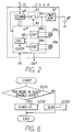
- the above-described nodes 2, 4, 6 and 8 respectively have an internal configuration shown in FIG. 2.
- each of the nodes 2, 4, 6 and 8 includes a communication circuit 48 for providing serial communications between the nodes through the communication network 10, a microprocessor 50 for processing the communications made through the communication circuit 48, for controlling its own controlled system or object, etc., a power circuit 52 for converting a voltage (normally 10V to 15V) produced from a vehicle battery BT to a predetermined source voltage (5V in the present embodiment) Vcc and supplying it to the communication circuit 48, the microprocessor 50 and the like, and a power control circuit 54 for controlling the supply of power from the power circuit 52 to the communication circuit 48 based on a command issued from the microprocessor 50.
- a communication circuit 48 for providing serial communications between the nodes through the communication network 10
- a microprocessor 50 for processing the communications made through the communication circuit 48, for controlling its own controlled system or object, etc.
- a power circuit 52 for converting a voltage (normally 10V to 15V) produced from a vehicle battery BT to a predetermined source voltage (5V in the present embodiment) V
- the communication circuit 48 sends transmit data outputted from the microprocessor 50 to the communication network 10 as a transmit signal and outputs an interrupt signal to the microprocessor 50 each time the communication circuit 48 receives a signal sent from the other nodes through the communication network 10 by a predetermined frame.
- the microprocessor 50 receives the interrupt signal from the communication circuit 48, the microprocessor 50 reads the data received by the communication circuit 48.
- each of the nodes 2, 4, 6 and 8 has two oscillating elements 56a and 56b as elements for generating clocks for activating the microprocessor 50.
- One oscillating element 56a generates a clock of a frequency (4 MHz in the present embodiment) sufficient for normal operation, whereas the other oscillating element 56b generates a clock of a frequency (30 kHz in the present embodiment) lower than the above frequency.
- the microprocessor 50 includes two oscillator circuits 58a and 58b for respectively oscillating the oscillating elements 56a and 56b and a selector 60 for activating either one of the oscillator circuits 58a and 58b and outputting a clock obtained from the activated oscillating circuit as an operating clock. Namely, the microprocessor 50 is able to switch its own operating clock to either one of 4 MHz and 30 kHz.
- the microprocessor 50 in each of the nodes 2, 4, 6 and 8 constructed in this way activates the oscillating element 56a and the oscillator circuit 58a to operate based on the clock of 4 MHz when the microprocessor 50 is placed in a normal mode for performing a normal operation, and gives a command to the power control circuit 54 so that the source voltage Vcc is supplied from the power circuit 52 to the communication circuit 48.
- the microprocessor 50 activates the oscillating element 56b and the oscillator circuit 58b to operate based on the clock of 30 kHz thereby to enter into a sleep mode in which power consumption is less provided. Further, the microprocessor 50 gives a command to the power control circuit 54 before entering into the sleep mode to reduce the supply of power from the power circuit 52 to the communication circuit 48.
- each of the nodes 2, 4, 6 and 8 is brought into the normal state when the microprocessor 50 is in operation in the normal mode.
- the microprocessor 50 enters the sleep mode the power consumed incident to the operation of the microprocessor 50 is reduced and the supply of the power to the communication circuit 48 is cut off. Therefore, the microprocessor 50 is brought into the sleep state corresponding to a state in which power consumption is extremely low.
- the nodes 2, 4, 6 and 8 respectively periodically transmit signals in predetermined periodic transmit periods or cycles of Ta through Td under normal conditions and send signals when some events have occurred such as state changes in input signals from switches.
- the signal transmitted by each of the nodes 2, 4, 6 and 8 has a frame structure shown in FIG. 4.
- one frame of the transmit signal is composed of a field SOF indicative of the head of the frame; a field ID indicative of a node name to receive the corresponding frame, the type of corresponding frame or the like; a field DATA indicative of a region for transmitting various data, switch signals and control signals or the like; a field CRC indicative of check data for detecting a communications error; a field ACK for allowing the node having received the corresponding frame to notify the completion of its reception to the node corresponding to the transmitting origin; and a field EOF indicative of the end of the frame.
- the DATA field in each of the signals transmitted by the nodes 2, 4, 6 and 8 includes a bit (hereinafter called “sleep disable bit”) SLNG used as a flag for notifying other nodes that the corresponding node is placed in a state (hereinafter called “sleep disable state”) of being unable to enter into the sleep state.
- SLNG a bit used as a flag for notifying other nodes that the corresponding node is placed in a state (hereinafter called “sleep disable state”) of being unable to enter into the sleep state.
- the node when the signal from the switch, which has been input to each of the nodes 2, 4, 6 and 8, is placed in a state in which each node has to perform some control and the corresponding node controls an actuator or the like, the node is in the sleep disable state, and hence sets the sleep disable bit SLNG to an active state ("1" in the present embodiment) indicative of the sleep disable state and transmits it therefrom. Otherwise, the node is in a sleep enable state. Thus, the node sets the sleep disable bit SLNG to an inactive state ("0" in the present embodiment) indicative of the sleep enable state.
- the A node (body ECU) 2 transmits a switch signal indicative of the turning on of the driver's seat door switch 34 while making the sleep disable bit SLNG active, thereby causing the B node (meter ECU) 4 to light the half-open door warning light 44.
- the sleep disable bit SLNG sent from each of other nodes is active even if each of the nodes 2, 4, 6 and 8 itself is in the sleep enable state, then the node does not proceed to the sleep state. Further, if each of the nodes 2, 4, 6 and 8 does not continuously receive therein the active sleep disable bits SLNG sent from other nodes for a predetermined period of time or more where each of the nodes 2, 4, 6 and 8 itself is placed in the sleep enable state, it makes the sleep disable bit SLNG inactive and transmits it therefrom, and all the nodes including the corresponding node itself are regarded as having been able to proceed to the sleep state and proceed from the normal state to the sleep state for the first time at that time.
- Step 110 the microprocessor 50 in each of the nodes 2, 4, 6 and 8 first executes a normal process for performing the periodic signal transmission and the signal transmission at the time of the occurrence of the event as shown in FIGS. 3A - 3D and performing control on its own controlled system or object.
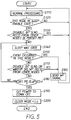
- the microprocessor 50 executes a setting process shown in FIG. 6 to thereby set a sleep disable bit SLNG in the signals to be transmitted active or inactive. Namely, it is first determined in S210 whether the node for such a microprocessor 50 itself is in the sleep enable state. If it is determined in S210 that the node is not in the sleep enable state, then the microprocessor 50 proceeds to S220 where the sleep disable bit SLNG is rendered active (set to 1). On the other hand, when the answer is determined to be YES in S210, the microprocessor 50 proceeds to S230 where the sleep disable bit SLNG is made inactive (set to 0).
- the microprocessor 50 proceeds to S120 where it makes a decision as to whether its own node is in the sleep enable state. If the answer is determined to be NO in S120, then the microprocessor 50 returns to S110. If the answer is determined to be YES in S120, then the microprocessor 50 proceeds to S130 where it makes a decision as to whether an active sleep disable bit SLNG sent from each of other nodes has been received within a predetermined time interval. If the answer is determined to be YES in S130, then the microprocessor 50 goes back to S110.
- the predetermined time interval determined in S130 is set to a time interval in which it is estimated that all the nodes other than the corresponding node will perform signal transmission once.
- the periodic transmit cycles Tb, Tc and Td of the B node 4, C node 6 and D node 8 are all equal to each other and only the periodic transmit cycle Ta of the A node 2 is set shorter than others as shown in FIGS. 3A - 3D. Therefore, the above-described predetermined time interval is set to a value larger than each of the periodic transmit cycles Tb through Td of the B node 4 through D node 8.
- the microprocessor 50 determines that all the nodes including its own node have been brought into the sleep enable state and proceeds to S140 where it shifts to a sleep waiting state in which the periodic transmission is stopped and only the receive operation is performed.
- the microprocessor 50 determines in S150 whether events (i.e., a change of state of each switch, etc.) have occurred in its own node. If the answer is determined to be YES in S150, then the microprocessor proceeds to S160 where it transmits a wakeup signal WP for notifying the resetting of itself to the normal state to other nodes and thereafter returns to S110 where the execution of the normal process is resumed.
- events i.e., a change of state of each switch, etc.
- the wakeup signal WP is disposed within the ID field shown in FIG. 4, for example, and transmitted.
- the wakeup signal WP does not influence a node that is performing the normal operation but has the function of allowing a node placed in the sleep waiting state or sleep state to perform the normal operation.
- the sleep disable bit SLNG may be rendered active and transmitted as an alternative to the wakeup signal WP.
- the microprocessor 50 proceeds to S170 where it is determined whether an active sleep disable bit SLNG sent from each of other nodes or the wakeup signal WP sent from each of other nodes has been received. Even when it is determined in S170 that either one of them has been received, the microprocessor 50 proceeds to S160 where the wakeup signal WP is transmitted. Thereafter, the microprocessor 50 returns to S110 where it resumes the execution of the normal process.
- the microprocessor 50 proceeds to S180 where it shifts to the sleep waiting state and determines whether a predetermined time interval has elapsed. If the answer is found to be NO in S180, then the microprocessor 50 returns to S140, whereas if the answer is found to be YES in S180, it proceeds to S190.
- the microprocessor 50 instructs the power control circuit 54 to reduce the supply of the power to the communication circuit 48.
- the microprocessor 50 deactivates the oscillating element 56a and the oscillator circuit 56a which have been oscillating up to that point, and activates the oscillating element 56b and the oscillating circuit 58b in place of them.
- the corresponding node is brought into the sleep state.
- the processes in S120, S150 and S210 correspond to a process which functions as a sleep determining means
- the process in S220 corresponds to a process which functions as a notifying or signaling means
- the processes in S130, S140 and S170 through S200 correspond to a process which functions as a switching means.
- the multiplex communication system 1 determines (in S120 and S210) whether each of the nodes 2, 4, 6 and 8 is in the sleep enable state. If it is determined that each node is not in the sleep enable state (i.e., if the answer is found to be NO in S120 and S210), then the node makes the sleep disable bit SLNG active and transmits it therefrom (S220) to thereby notify its own sleep disable state to all the other nodes.
- the node stops the transmission of the active sleep disable bit SLNG (S230). If it is determined that the active sleep disable bit SLNG sent from each of other nodes has not been received continuously for the predetermined time interval or more (i.e., if the answer is found to be NO in S130), then all the nodes including the corresponding node are determined to have been brought into the sleep enable state and proceed to the sleep waiting state. Thereafter, the operating state of the corresponding node is switched to the sleep state (S190 and S200).
- a tester or the like for checking each node and the state of communications cannot determine or detect whether other nodes are in the sleep waiting state or in the sleep state or they are not under transmission due to the absence of a signal to be transmitted even though they are in the normal state. Therefore, in order to cause other nodes to determine when the operating state is shifted to another state, a signal for notifying a shift to the sleep waiting state and a signal for notifying a shift to the sleep state are determined in advance. Further, the signals may be respectively transmitted when it is determined in S130 that the predetermined time interval has elapsed and the microprocessor 50 proceeds to S140 and when it is determined in S180 that the predetermined time interval has elapsed and the microprocessor 50 proceeds to S190.
- the nodes 2, 4, 6 and 8 can mutually check, based on the decision that the active sleep disable bits SLNG have not been sent from other nodes, whether they have been brought into the sleep enable state. Therefore, each node can be reliably shifted to the sleep state without discriminating between communicable nodes and the need for a complex determining process as in the above-described conventional system even if nodes capable of performing transmit operations due to failures or the like exist. Accordingly, a vehicle prone to having dead batteries can reliably reduce power to be used up by the battery BT.
- each of the nodes 2, 4, 6 and 8 is constructed to proceed to the sleep state by simply determining that no active sleep disable bits SLNG are sent from other nodes, nodes can be additionally provided without a change in determining process for shifting to the sleep state and hence the system has excellent expandability.
- the multiplex communication system when all the nodes enter into the sleep enable state (i.e., when the answer is determined as negative in S130), they first proceed to the sleep waiting state without immediately entering into the sleep state and then execute the processes of S140 through S180. Thus, each node enters into the sleep state after it is confirmed that the node is in the sleep enable state and the state in which the sleep disable bits SLNG are not sent from other nodes continue over the predetermined time interval. Therefore, the multiplex communication system according to the present embodiment can more reliably determine whether each node should shift to the sleep state.
- each of the nodes 2, 4, 6 and 8 in the multiplex communication system 1 according to the present embodiment is brought into the sleep state as described above, i.e., when the microprocessor 50 enters into the sleep mode, the microprocessor 50 is activated based on the slow clock of 30 kHz to detect the state of the signal directly inputted from each switch or the like and the state of the communication network 10.
- the microprocessor 50 detects changes in the states, the microprocessor 50 starts (wakes up) the entire system.
- a process executed by the microprocessor 50 included in each of the nodes 2, 4, 6 and 8 upon transition of the microprocessor 50 to the sleep mode will next be described with reference to a flowchart shown in FIG. 7.
- the microprocessor 50 When each individual node 2, 4, 6 or 8 enters into a sleep state as shown in FIG. 7, the microprocessor 50 first determines in S310 whether an event (i.e., a change of state of each switch or the like other than the communication network 10) has occurred in its own node. If the answer is found to be NO in S310, then the microprocessor 50 proceeds to S320 where it is determined whether a communication signal is produced in the communication network 10. If it is determined in S320 that the communication signal has not been produced, then the microprocessor 50 returns to S310.
- an event i.e., a change of state of each switch or the like other than the communication network
- the microprocessor 50 instructs the power control circuit 54 to supply the source voltage Vcc from the power circuit 52 to the communication circuit 48, thereby returning the corresponding node to the communicable normal state.
- the microprocessor 50 sends the above-described wakeup signal WP twice in S350 to return other nodes from the sleep state to the normal state.
- the first wakeup signal WP transmitted in S350 serves to shift all other nodes from the sleep state to a receivable state.
- the second wakeup signal WP serves to notify a receivable state of the node of the microprocessor 50 to the nodes brought into the receivable state by the first wakeup signal WP.
- the microprocessor 50 proceeds to S360 where it enters into a transmit waiting state in which only the receive operation is performed.
- the first wakeup signal WP of the wakeup signals WP transmitted twice in S350 is detected by the process in S320 at other nodes. Other nodes transmit the wakeup signals WP as will be described later. Therefore, when the microprocessor is in the transmit waiting state, the microprocessor 50 first determines in S370 whether wakeup signals WP sent from all the nodes other than its own node have been received. If the answer is found to be NO in S370, then the microprocessor 50 proceeds to S380 where it is determined whether a predetermined time interval has elapsed since it has entered into the transmit waiting state. If the answer is found to be NO in S380, then the microprocessor 50 returns to S360.
- the communication circuit 48 starts operating from the time when supplied with the source voltage Vcc and outputs an interrupt signal to the microprocessor 50 each time the communication circuit 48 receives therein the signal sent from each of other nodes by the predetermined frame, as already described above. Since the microprocessor 50 reads the received data from the communication circuit 48 when the microprocessor 50 receives the interrupt signal from the communication circuit 48, the operation for receiving the wakeup signals WP from other nodes can be done immediately after the supply of the source voltage Vcc to the communication circuit 48. Thus, the process in S370 makes a decision, based on the received data read as described above and sent from the communication circuit 48, as to whether or not the wakeup signal WP has been sent from any of the nodes.
- the routine procedure proceeds to S390 where it is determined whether it is necessary to transmit an event frame with a switch signal or the like disposed therein to the DATA frame shown in FIG. 4. If the answer is found to be YES in S390, then the execution of the normal process (S110) is resumed in S400 after transmission of the event frame. If the answer is found to be NO in S390, then the execution of the normal process is resumed as it is.
- the microprocessor 50 instructs the power control circuit 54 to supply the source voltage Vcc from the power circuit 52 to the communication circuit 48.
- the corresponding node is returned to the communicable normal state at the time that the process in S420 has been finished.
- the microprocessor 50 transmits the wakeup signal WP to notify its own startup to other nodes, followed by proceeding to S360 where the above-described processes (S360 through S400) are executed and thereafter the execution of the normal process (S110) is resumed.
- the process in S310 corresponds to a process which serves as a start condition determining means
- the processes in S330 through S350 correspond to a process which functions as a first starting means
- the process in S320 corresponds to a process which serves as a start signal detecting means
- the processes in S410 through S430 correspond to a process which functions as a second starting means
- the processes in S360 through S380 correspond to a process which works as a transmit permitting means.
- start node when it is determined by the process in S310 that the event has occurred in any of the nodes while all the nodes 2, 4, 6 and 8 are in the sleep state, the corresponding node (hereinafter called "start node") is returned from the sleep state in which the microprocessor operates based on the low-speed clock of 30 kHz to the normal state in which the microprocessor operates based on the high-speed clock of 4 MHz in accordance with the processes of S330 to S350 and transmits the wakeup signal WP used as a start signal twice.
- each of other nodes other than the start node detects the first wakeup signal WP of the wakeup signals WP transmitted twice as described above in accordance with the process in S320.
- each of the nodes other than the start node is returned from the sleep state to the normal state in accordance with the processes of S410 to S430 and the corresponding node itself transmits the wakeup signal WP.
- All the nodes including the start node are returned from the sleep state to the normal state as described above and thereafter temporarily enter into the transmit waiting state in which only the receive operation is performed. If it is determined based on the processes of S360 through S380 that the wakeup signals WP sent from all the nodes other than the corresponding node itself have been received or that the predetermined time interval has elapsed, it is determined that all the nodes have been brought into the receivable state (transmit waiting state). Thus, the operation of transmission of a desired signal from the corresponding node is allowed and the desired signal (event frame) is transmitted if necessary in accordance with the processes in S390 and S400.
- each of the nodes other than the start node is returned from the sleep state to the normal state in response to the first wakeup signal WP sent from the start node, there is a possibility that the first wakeup signal WP cannot be received by the node due to its return delay. Even in such a case, each of the nodes other than the start node reliably receives the second wakeup signal WP sent from the start node, thereby making it possible to detect that the start node is in the receivable state (transmit waiting state).
- the node i.e., start node that has detected the change of state of the switch (the occurrence of the event) in S310 to start the entire system, transmits a switch signal indicative of the change of state of the switch in the form of the event frame.
- the start node transmits the event frame in S400 when data to be transmitted is produced due to the change of state of the switch or the like, which has been input thereto.
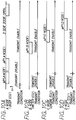
- FIGS. 8A - 10D Operation based on the execution of the processes shown in FIG. 7 will now be described with reference to FIGS. 8A - 10D by taking as an example the case in which the driver's seat door is opened when all the nodes 2, 4, 6 and 8 are respectively in the sleep state.
- the driver's seat door switch 34 changes from an off to an on state as shown in FIG. 8A.
- the A node (body ECU) 2 detects its change (i.e., the answer is found to be YES in S310) and the operating clock of the microprocessor 50 is switched from the low-speed clock (on-sleep mode clock) of 30 kHz to the high-speed clock (on-normal mode clock) of 4 MHz. Further, the source voltage Vcc is supplied to the communication circuit 48. As a result, the A node 2 is returned to the communicable normal state (S330 and S340). Next, the A node 2 transmits the wakeup signal WP to the communication network 10 (transmission line) twice to start up other nodes 4, 6 and 8 (S350).
- the signal sent through the driver's seat door switch 34 is inputted to an input port of the microprocessor 50 of the A node 2. Further, the microprocessor 50 of the A node 2 samples the signal inputted to the input port thereof in a predetermined cycle as indicated by upward arrows in FIG. 8C to thereby detect the change of state of the driver's seat door switch 34.
- the nodes 4, 6 and 8 other than the A node 2 first detect the first wakeup signal WP sent from the A node 2 (i.e., the answer is found to be YES in S320) as shown in FIGS. 9A - 9D. In doing so, the operating clock of the microprocessor 50 in each of the nodes 4, 6 and 8 is switched from the on-sleep mode clock to the on-normal mode clock and the source voltage Vcc is supplied to the communication circuit 48. As a result, the individual nodes 4, 6 and 8 other than the A node 2 are also returned to the communicable normal state (S410 and S420).
- the microprocessor 50 monitors a change in the level of the communication network 10 through the normal input port thereof.
- Upward arrows in FIGS. 9C show sampling timing provided to detect the change in the level of the communication network 10 by the microprocessor 50.
- the A node 2 receives therein the respective wakeup signals WP sent from other nodes 4, 6 and 8 and other nodes 4, 6 and 8 also respectively receive therein respective wakeup signals WP sent from nodes other than themselves.
- the respective nodes 2, 4, 6 and 8 determine that all the nodes constituting the system have been brought into a receivable state (i.e., the answer is found to be YES in S370).
- the A node 2 determines as necessary to transmit an event frame (i.e., the answer is found to be YES in S390) and transmits an event frame including a switch signal (the "D-seat door opening" field in FIG. 10A) indicative of the turning on of the driver's seat door switch 34 (S400).
- the B node (meter ECU) 4 receives therein the event frame sent from the A node 2 to turn on the half-open door warning light 44 in the meter panel.
- an arrow indicated at a time t1 in FIG. 10A shows timing in which the driver's seat door is opened.
- the node (start node) which has determined that the event for starting the corresponding system has occurred is first returned from the sleep state to the normal state and transmits the wakeup signal WP therefrom twice. Further, the node returns all the other nodes from the sleep state to the normal state based on the first wakeup signal WP of the twice-transmitted wakeup signals WP. When the respective nodes other than the start node are also returned to the normal state, they send the wakeup signals WP respectively. When all the nodes including the start node all receive therein the wakeup signals WP sent from other nodes other than themselves, it is determined that all the nodes have been returned to the normal state, and the operation of transmission of the desired signals is started.
- each node can reliably proceed to the sleep state. Further, when the individual nodes restart from the sleep state, the respective nodes 2, 4, 6 and 8 start to transmit the desired signals after having confirmed that all the nodes have completely been returned to the normal state. Therefore, when the individual nodes restart from the sleep state, they can reliably communicate with one another without missing reception of the communication signals.
- the node (start node) firstly returned from the sleep state to the normal state transmits the wakeup signal WP twice. Therefore, other nodes can reliably receive the second wakeup signal WP even if they cannot receive the first wakeup signal WP sent from the start node. Thus, all the nodes 2, 4, 6 and 8 can reliably check or detect that they have been returned to the normal state, to be able to start the transmission of the desired signals.
- the operation of transmission of the desired signals from its own nodes is permitted after elapse of the predetermined time interval (i.e., the answer is found to be YES in S380).
- the multiplex communication system 1 of this embodiment since the operation of transmission of desired signals from other nodes is allowed even if any node cannot transmit the wakeup signal WP due to its failure or the like, it is possible to ensure communications made between the normal nodes.
- the microprocessor 50 when each of the nodes 2, 4, 6 and 8 is kept in the sleep state, the microprocessor 50 is activated based on the clock (30 kHz) whose frequency is low and detects the change of state of the switch or the communication network 10 through its normal input port.
- the microprocessor 50 may be constructed to stop its operating clock when each node is in the sleep state. In this case, when the state of the communication network 10 or the signal sent from the switch changes, each node may be set to return to the normal state by externally interrupting the microprocessor 50.
- each node may be returned from the sleep state to the normal state by externally interrupting the microprocessor when the state of the switch or the communication network 10 changes.
- the multiplex communication system 1 has been described in detail in connection with the case in which all the nodes are able to proceed to the sleep state.
- the multiplex communication system 1 is not necessarily limited to this arrangement.
- the multiplex communication system 1 may be constructed by connecting nodes or the like (corresponding to nodes configured to be unable to proceed to the sleep state) activated only when a normally-operated node or an ignition key is operated.
- the communications similar to the aforementioned embodiment are made between the nodes constructed to be able to shift to the sleep state.
Landscapes
- Engineering & Computer Science (AREA)
- Computer Networks & Wireless Communication (AREA)
- Signal Processing (AREA)
- Selective Calling Equipment (AREA)
- Small-Scale Networks (AREA)
Applications Claiming Priority (3)
| Application Number | Priority Date | Filing Date | Title |
|---|---|---|---|
| JP288970/95 | 1995-11-07 | ||
| JP28897095 | 1995-11-07 | ||
| JP28897095A JP3463433B2 (ja) | 1995-11-07 | 1995-11-07 | 多重通信システム |
Publications (3)
| Publication Number | Publication Date |
|---|---|
| EP0773650A2 true EP0773650A2 (fr) | 1997-05-14 |
| EP0773650A3 EP0773650A3 (fr) | 1999-05-19 |
| EP0773650B1 EP0773650B1 (fr) | 2004-05-26 |
Family
ID=17737164
Family Applications (1)
| Application Number | Title | Priority Date | Filing Date |
|---|---|---|---|
| EP96117788A Expired - Lifetime EP0773650B1 (fr) | 1995-11-07 | 1996-11-06 | Système de communication multiplexé réparti avec mode dormant à haute réaction |
Country Status (4)
| Country | Link |
|---|---|
| US (1) | US5757773A (fr) |
| EP (1) | EP0773650B1 (fr) |
| JP (1) | JP3463433B2 (fr) |
| DE (1) | DE69632565T2 (fr) |
Cited By (12)
| Publication number | Priority date | Publication date | Assignee | Title |
|---|---|---|---|---|
| WO1999046888A1 (fr) * | 1998-03-10 | 1999-09-16 | Koninklijke Philips Electronics N.V. | Systeme de transmission de donnees |
| EP0917991A3 (fr) * | 1997-11-21 | 2000-11-08 | SUMITOMO WIRING SYSTEMS, Ltd. | Système de communication multiplexé de vehicule et méthode de fabrication |
| WO2002076794A3 (fr) * | 2001-03-08 | 2003-03-20 | Siemens Vdo Automotive Corp | Systeme d'eveil pour composant electronique embarque dans un vehicule |
| WO2003104037A1 (fr) | 2002-06-10 | 2003-12-18 | Philips Intellectual Property & Standards Gmbh | Procede et systeme pour le passage d'un mode de fonctionnement sous-reseau a un mode de fonctionnement reseau complet |
| EP1158718A3 (fr) * | 2000-05-24 | 2004-11-10 | General Motors Corporation | Système de gestion de réseaux utilisant des réseaux virtuels dans un véhicule |
| WO2005115801A1 (fr) | 2004-05-19 | 2005-12-08 | Bendix Commercial Vehicle Systems Llc | Module d'activation de fonction |
| WO2006005437A1 (fr) * | 2004-07-09 | 2006-01-19 | Daimlerchrysler Ag | Systeme de commande et d'affichage pour vehicule automobile |
| DE10136036B4 (de) * | 2000-07-27 | 2010-06-17 | DENSO CORPORATION, Kariya-shi | Verfahren und System zum Erfassen von Abnormitäten mit einer Sleep-Modus-Prüffunktion |
| EP2538609A1 (fr) * | 2011-06-22 | 2012-12-26 | Siemens Aktiengesellschaft | Economie d'énergie dans un noeud de réseau d'un réseau d'automatisation |
| WO2013153151A1 (fr) * | 2012-04-14 | 2013-10-17 | Volkswagen Aktiengesellschaft | Dispositif, procédé et programme d'ordinateur pour exploiter un système de bus de données d'un véhicule automobile |
| WO2014056557A1 (fr) * | 2012-10-12 | 2014-04-17 | Audi Ag | Procédé d'établissement d'une communication avec une unité de commande, unité de commande et véhicule |
| CN115667772A (zh) * | 2020-07-13 | 2023-01-31 | 太阳Hst株式会社 | 工业用充电式无线电磁阀系统 |
Families Citing this family (27)
| Publication number | Priority date | Publication date | Assignee | Title |
|---|---|---|---|---|
| GB9721777D0 (en) * | 1997-10-15 | 1997-12-10 | Jaguar Cars | Immobilisation system for motor vehicles |
| JP3566846B2 (ja) | 1997-12-24 | 2004-09-15 | 古河電気工業株式会社 | 多重通信方法 |
| US6662234B2 (en) * | 1998-03-26 | 2003-12-09 | National Semiconductor Corporation | Transmitting data from a host computer in a reduced power state by an isolation block that disconnects the media access control layer from the physical layer |
| US6374161B1 (en) | 1999-04-26 | 2002-04-16 | Denso Corporation | Automobile control system and method capable of revising control data transmission function |
| US6584573B1 (en) | 1999-08-30 | 2003-06-24 | Intel Corporation | Placing a computer system into a sleeping state |
| US6523128B1 (en) * | 1999-08-31 | 2003-02-18 | Intel Corporation | Controlling power for a sleeping state of a computer to prevent overloading of the stand-by power rails by selectively asserting a control signal |
| GB2360670B (en) * | 2000-03-22 | 2004-02-04 | At & T Lab Cambridge Ltd | Power management system |
| JP3578058B2 (ja) * | 2000-07-13 | 2004-10-20 | 株式会社デンソー | 多重通信システム |
| KR20040002383A (ko) * | 2001-04-27 | 2004-01-07 | 미쯔비시 지도샤 고교 가부시끼가이샤 | 차량용 다중통신 장치 |
| JP3797166B2 (ja) * | 2001-09-18 | 2006-07-12 | 株式会社デンソー | ネットワークシステム |
| US20030223387A1 (en) * | 2002-05-31 | 2003-12-04 | Davenport David Michael | Remote vehicle communication associate |
| JP4551695B2 (ja) * | 2004-05-25 | 2010-09-29 | シャープ株式会社 | 警報システムおよび警報装置 |
| EP1938158B1 (fr) * | 2005-07-04 | 2010-05-26 | VKR Holding A/S | Systeme et procede de gestion d'execution de commande |
| JP4548260B2 (ja) * | 2005-07-27 | 2010-09-22 | 株式会社デンソー | 車両用通信システム |
| JP4783643B2 (ja) * | 2006-02-06 | 2011-09-28 | 株式会社小松製作所 | 移動体監視装置および移動体監視システム |
| JP2008074230A (ja) * | 2006-09-21 | 2008-04-03 | Nissan Motor Co Ltd | 車両用無線通信システムおよび車両用無線通信方法 |
| JP4866214B2 (ja) * | 2006-11-17 | 2012-02-01 | 株式会社オートネットワーク技術研究所 | 制御ユニットおよび車載用の多重通信システム |
| JP4775448B2 (ja) * | 2009-01-27 | 2011-09-21 | ブラザー工業株式会社 | 通信装置 |
| DE102009015197A1 (de) * | 2009-03-31 | 2010-10-14 | Volkswagen Ag | Steuergerät für ein Fahrzeugnetzwerk und Verfahren zum Betreiben eines Fahrzeugnetzwerkes |
| DE102010032993B3 (de) | 2010-07-31 | 2011-12-08 | Audi Ag | Verfahren zum Betreiben eines Bussteuergeräts sowie Bussteuergerät |
| JP5598429B2 (ja) * | 2011-06-22 | 2014-10-01 | 株式会社オートネットワーク技術研究所 | 電源制御システム、電源制御装置及び電源制御方法 |
| JP2013058906A (ja) * | 2011-09-08 | 2013-03-28 | Denso Corp | 通信ネットワークシステム |
| JP5568528B2 (ja) * | 2011-08-23 | 2014-08-06 | 本田技研工業株式会社 | 電力線通信システム |
| JP5617875B2 (ja) | 2012-08-10 | 2014-11-05 | 株式会社デンソー | 車載ネットワークシステム |
| JP6040952B2 (ja) * | 2014-04-04 | 2016-12-07 | 株式会社デンソー | 通信システム、電子制御装置 |
| DE102019200955A1 (de) * | 2019-01-25 | 2020-07-30 | Robert Bosch Gmbh | Verfahren zur Aktivierung und Deaktivierung eines Steuergeräts |
| KR102872210B1 (ko) * | 2019-12-17 | 2025-10-16 | 현대자동차주식회사 | 차량용 캔 네트워크 슬립 진단 장치 및 그의 캔 네트워크 슬립 진단 방법 |
Citations (2)
| Publication number | Priority date | Publication date | Assignee | Title |
|---|---|---|---|---|
| JPH04292236A (ja) | 1991-03-19 | 1992-10-16 | Daihatsu Motor Co Ltd | 車両用多重通信システム |
| JPH0638276A (ja) | 1992-07-17 | 1994-02-10 | Mazda Motor Corp | 多重伝送装置 |
Family Cites Families (9)
| Publication number | Priority date | Publication date | Assignee | Title |
|---|---|---|---|---|
| FR2626998B1 (fr) * | 1988-02-05 | 1990-08-03 | Bendix Electronics Sa | Systeme de mise en etat operationnel et en etat de veille de boitiers electroniques connectes a un canal de communication |
| US5351041A (en) * | 1990-10-25 | 1994-09-27 | Pioneer Electronic Corporation | Method of data communication in communication network on automobile |
| JP2949998B2 (ja) * | 1992-02-21 | 1999-09-20 | 日産自動車株式会社 | 通信装置 |
| US5594735A (en) * | 1992-04-10 | 1997-01-14 | Nec Corporation | TDMA mobile unit frequency synthesizer having power saving mode during transmit and receive slots |
| US5404544A (en) * | 1992-06-05 | 1995-04-04 | Advanced Micro Devices | System for periodically transmitting signal to/from sleeping node identifying its existence to a network and awakening the sleeping node responding to received instruction |
| JP3299600B2 (ja) * | 1993-07-19 | 2002-07-08 | マツダ株式会社 | 多重伝送装置 |
| KR100346503B1 (ko) * | 1994-07-21 | 2002-11-22 | 인터디지탈 테크날러지 코포레이션 | 통신시스템 가입자 유니트용 전력소비 제어방법 및 장치 |
| JPH0870312A (ja) * | 1994-08-26 | 1996-03-12 | Furukawa Electric Co Ltd:The | 多重伝送方法及び多重端末装置 |
| US5691980A (en) * | 1995-06-07 | 1997-11-25 | General Electric Company | Local communication network for power reduction and enhanced reliability in a multiple node tracking system |
-
1995
- 1995-11-07 JP JP28897095A patent/JP3463433B2/ja not_active Expired - Lifetime
-
1996
- 1996-11-06 EP EP96117788A patent/EP0773650B1/fr not_active Expired - Lifetime
- 1996-11-06 US US08/744,579 patent/US5757773A/en not_active Expired - Lifetime
- 1996-11-06 DE DE69632565T patent/DE69632565T2/de not_active Expired - Lifetime
Patent Citations (2)
| Publication number | Priority date | Publication date | Assignee | Title |
|---|---|---|---|---|
| JPH04292236A (ja) | 1991-03-19 | 1992-10-16 | Daihatsu Motor Co Ltd | 車両用多重通信システム |
| JPH0638276A (ja) | 1992-07-17 | 1994-02-10 | Mazda Motor Corp | 多重伝送装置 |
Cited By (19)
| Publication number | Priority date | Publication date | Assignee | Title |
|---|---|---|---|---|
| EP0917991A3 (fr) * | 1997-11-21 | 2000-11-08 | SUMITOMO WIRING SYSTEMS, Ltd. | Système de communication multiplexé de vehicule et méthode de fabrication |
| US6327263B1 (en) | 1997-11-21 | 2001-12-04 | Harness System Technologies | On-vehicle multiplex communication system and manufacturing method thereof |
| WO1999046888A1 (fr) * | 1998-03-10 | 1999-09-16 | Koninklijke Philips Electronics N.V. | Systeme de transmission de donnees |
| EP1158718A3 (fr) * | 2000-05-24 | 2004-11-10 | General Motors Corporation | Système de gestion de réseaux utilisant des réseaux virtuels dans un véhicule |
| DE10136036B4 (de) * | 2000-07-27 | 2010-06-17 | DENSO CORPORATION, Kariya-shi | Verfahren und System zum Erfassen von Abnormitäten mit einer Sleep-Modus-Prüffunktion |
| US6838783B2 (en) | 2001-03-08 | 2005-01-04 | Siemens Vdo Automotive Corporation | Wake up system for electronic component supported on a vehicle |
| WO2002076794A3 (fr) * | 2001-03-08 | 2003-03-20 | Siemens Vdo Automotive Corp | Systeme d'eveil pour composant electronique embarque dans un vehicule |
| WO2003104037A1 (fr) | 2002-06-10 | 2003-12-18 | Philips Intellectual Property & Standards Gmbh | Procede et systeme pour le passage d'un mode de fonctionnement sous-reseau a un mode de fonctionnement reseau complet |
| WO2003104036A1 (fr) * | 2002-06-10 | 2003-12-18 | Philips Intellectual Property & Standards Gmbh | Procede et systeme pour le passage d'un mode de fonctionnement sous-reseau a un mode de fonctionnement reseau complet |
| US8566466B2 (en) | 2002-06-10 | 2013-10-22 | Nxp B.V. | Method and system for switching between subnetwork operation and full network operation |
| WO2005115801A1 (fr) | 2004-05-19 | 2005-12-08 | Bendix Commercial Vehicle Systems Llc | Module d'activation de fonction |
| US7274977B2 (en) | 2004-05-19 | 2007-09-25 | Bendix Commercial Vehicle Systems Llc | Feature enabling unit |
| US7729813B2 (en) | 2004-05-19 | 2010-06-01 | Bendix Commerical Vehicle Systems Llc | Feature enabler unit |
| WO2006005437A1 (fr) * | 2004-07-09 | 2006-01-19 | Daimlerchrysler Ag | Systeme de commande et d'affichage pour vehicule automobile |
| EP2538609A1 (fr) * | 2011-06-22 | 2012-12-26 | Siemens Aktiengesellschaft | Economie d'énergie dans un noeud de réseau d'un réseau d'automatisation |
| WO2013153151A1 (fr) * | 2012-04-14 | 2013-10-17 | Volkswagen Aktiengesellschaft | Dispositif, procédé et programme d'ordinateur pour exploiter un système de bus de données d'un véhicule automobile |
| US9632970B2 (en) | 2012-04-14 | 2017-04-25 | Volkswagen Ag | Device, method and computer program for operating a data bus system of a motor vehicle |
| WO2014056557A1 (fr) * | 2012-10-12 | 2014-04-17 | Audi Ag | Procédé d'établissement d'une communication avec une unité de commande, unité de commande et véhicule |
| CN115667772A (zh) * | 2020-07-13 | 2023-01-31 | 太阳Hst株式会社 | 工业用充电式无线电磁阀系统 |
Also Published As
| Publication number | Publication date |
|---|---|
| JPH09135257A (ja) | 1997-05-20 |
| DE69632565T2 (de) | 2005-06-02 |
| JP3463433B2 (ja) | 2003-11-05 |
| EP0773650A3 (fr) | 1999-05-19 |
| DE69632565D1 (de) | 2004-07-01 |
| EP0773650B1 (fr) | 2004-05-26 |
| US5757773A (en) | 1998-05-26 |
Similar Documents
| Publication | Publication Date | Title |
|---|---|---|
| US5757773A (en) | Multiplex distributed communication system having high sleep mode responsiveness | |
| US6898499B2 (en) | Control system | |
| KR101393539B1 (ko) | 자동차 통합 네트워크 시스템 | |
| JP4046776B2 (ja) | データ伝送システム | |
| US5633537A (en) | Multiplex transmission apparatus | |
| US20140350772A1 (en) | Vehicle diagnostic system | |
| JP5120720B2 (ja) | 電子制御装置及び電子制御装置の制御方法 | |
| JP3797166B2 (ja) | ネットワークシステム | |
| JP3566846B2 (ja) | 多重通信方法 | |
| US9817707B2 (en) | Controller for reducing power | |
| JP4866214B2 (ja) | 制御ユニットおよび車載用の多重通信システム | |
| JP3256920B2 (ja) | 多重伝送装置 | |
| KR20120018648A (ko) | 캔 버스에 연결된 차량용 전장 유니트 및 상기 유니트를 웨이크-업 하는 방법 | |
| JP2014165837A (ja) | 通信ノード | |
| JPH06292274A (ja) | 多重通信装置 | |
| US20050027898A1 (en) | Method of control of the different operating states of a data bus system | |
| KR20190112478A (ko) | 슬립 모드에서의 차량 배터리 전원 관리 방법 및 장치 | |
| JP5028973B2 (ja) | 通信システムの制御方法、通信装置及び通信システム | |
| JP2004254043A (ja) | 車両内ネットワーク制御装置 | |
| JP3901539B2 (ja) | 多重通信装置の起動方法 | |
| JPH09237239A (ja) | 多重伝送装置 | |
| JP2950085B2 (ja) | 移動体用多重通信装置 | |
| JP3250323B2 (ja) | 車両用診断システム | |
| JP2017220831A (ja) | 通信装置 | |
| JP2008277975A (ja) | 中継接続ユニット |
Legal Events
| Date | Code | Title | Description |
|---|---|---|---|
| PUAI | Public reference made under article 153(3) epc to a published international application that has entered the european phase |
Free format text: ORIGINAL CODE: 0009012 |
|
| AK | Designated contracting states |
Kind code of ref document: A2 Designated state(s): DE FR GB |
|
| PUAL | Search report despatched |
Free format text: ORIGINAL CODE: 0009013 |
|
| AK | Designated contracting states |
Kind code of ref document: A3 Designated state(s): DE FR GB |
|
| 17P | Request for examination filed |
Effective date: 19990527 |
|
| 17Q | First examination report despatched |
Effective date: 20020809 |
|
| GRAH | Despatch of communication of intention to grant a patent |
Free format text: ORIGINAL CODE: EPIDOS IGRA |
|
| GRAS | Grant fee paid |
Free format text: ORIGINAL CODE: EPIDOSNIGR3 |
|
| GRAA | (expected) grant |
Free format text: ORIGINAL CODE: 0009210 |
|
| AK | Designated contracting states |
Kind code of ref document: B1 Designated state(s): DE FR GB |
|
| REG | Reference to a national code |
Ref country code: GB Ref legal event code: FG4D |
|
| REF | Corresponds to: |
Ref document number: 69632565 Country of ref document: DE Date of ref document: 20040701 Kind code of ref document: P |
|
| ET | Fr: translation filed | ||
| REG | Reference to a national code |
Ref country code: GB Ref legal event code: 746 Effective date: 20050210 |
|
| PLBE | No opposition filed within time limit |
Free format text: ORIGINAL CODE: 0009261 |
|
| STAA | Information on the status of an ep patent application or granted ep patent |
Free format text: STATUS: NO OPPOSITION FILED WITHIN TIME LIMIT |
|
| 26N | No opposition filed |
Effective date: 20050301 |
|
| REG | Reference to a national code |
Ref country code: FR Ref legal event code: PLFP Year of fee payment: 20 |
|
| PGFP | Annual fee paid to national office [announced via postgrant information from national office to epo] |
Ref country code: DE Payment date: 20151119 Year of fee payment: 20 Ref country code: GB Payment date: 20151118 Year of fee payment: 20 |
|
| PGFP | Annual fee paid to national office [announced via postgrant information from national office to epo] |
Ref country code: FR Payment date: 20151119 Year of fee payment: 20 |
|
| REG | Reference to a national code |
Ref country code: DE Ref legal event code: R071 Ref document number: 69632565 Country of ref document: DE |
|
| REG | Reference to a national code |
Ref country code: GB Ref legal event code: PE20 Expiry date: 20161105 |
|
| PG25 | Lapsed in a contracting state [announced via postgrant information from national office to epo] |
Ref country code: GB Free format text: LAPSE BECAUSE OF EXPIRATION OF PROTECTION Effective date: 20161105 |