EP0774786A2 - CMOS-Halbleiter-Bauteil - Google Patents
CMOS-Halbleiter-Bauteil Download PDFInfo
- Publication number
- EP0774786A2 EP0774786A2 EP96118200A EP96118200A EP0774786A2 EP 0774786 A2 EP0774786 A2 EP 0774786A2 EP 96118200 A EP96118200 A EP 96118200A EP 96118200 A EP96118200 A EP 96118200A EP 0774786 A2 EP0774786 A2 EP 0774786A2
- Authority
- EP
- European Patent Office
- Prior art keywords
- type
- type mosfet
- mosfet
- source
- semiconductor device
- Prior art date
- Legal status (The legal status is an assumption and is not a legal conclusion. Google has not performed a legal analysis and makes no representation as to the accuracy of the status listed.)
- Withdrawn
Links
Images


Classifications
-
- G—PHYSICS
- G09—EDUCATION; CRYPTOGRAPHY; DISPLAY; ADVERTISING; SEALS
- G09G—ARRANGEMENTS OR CIRCUITS FOR CONTROL OF INDICATING DEVICES USING STATIC MEANS TO PRESENT VARIABLE INFORMATION
- G09G3/00—Control arrangements or circuits, of interest only in connection with visual indicators other than cathode-ray tubes
- G09G3/04—Control arrangements or circuits, of interest only in connection with visual indicators other than cathode-ray tubes for presentation of a single character by selection from a plurality of characters, or by composing the character by combination of individual elements, e.g. segments using a combination of such display devices for composing words, rows or the like, in a frame with fixed character positions
- G09G3/16—Control arrangements or circuits, of interest only in connection with visual indicators other than cathode-ray tubes for presentation of a single character by selection from a plurality of characters, or by composing the character by combination of individual elements, e.g. segments using a combination of such display devices for composing words, rows or the like, in a frame with fixed character positions by control of light from an independent source
- G09G3/18—Control arrangements or circuits, of interest only in connection with visual indicators other than cathode-ray tubes for presentation of a single character by selection from a plurality of characters, or by composing the character by combination of individual elements, e.g. segments using a combination of such display devices for composing words, rows or the like, in a frame with fixed character positions by control of light from an independent source using liquid crystals
-
- H—ELECTRICITY
- H10—SEMICONDUCTOR DEVICES; ELECTRIC SOLID-STATE DEVICES NOT OTHERWISE PROVIDED FOR
- H10D—INORGANIC ELECTRIC SEMICONDUCTOR DEVICES
- H10D84/00—Integrated devices formed in or on semiconductor substrates that comprise only semiconducting layers, e.g. on Si wafers or on GaAs-on-Si wafers
- H10D84/80—Integrated devices formed in or on semiconductor substrates that comprise only semiconducting layers, e.g. on Si wafers or on GaAs-on-Si wafers characterised by the integration of at least one component covered by groups H10D12/00 or H10D30/00, e.g. integration of IGFETs
- H10D84/82—Integrated devices formed in or on semiconductor substrates that comprise only semiconducting layers, e.g. on Si wafers or on GaAs-on-Si wafers characterised by the integration of at least one component covered by groups H10D12/00 or H10D30/00, e.g. integration of IGFETs of only field-effect components
- H10D84/83—Integrated devices formed in or on semiconductor substrates that comprise only semiconducting layers, e.g. on Si wafers or on GaAs-on-Si wafers characterised by the integration of at least one component covered by groups H10D12/00 or H10D30/00, e.g. integration of IGFETs of only field-effect components of only insulated-gate FETs [IGFET]
- H10D84/85—Complementary IGFETs, e.g. CMOS
- H10D84/857—Complementary IGFETs, e.g. CMOS comprising an N-type well but not a P-type well
-
- H—ELECTRICITY
- H10—SEMICONDUCTOR DEVICES; ELECTRIC SOLID-STATE DEVICES NOT OTHERWISE PROVIDED FOR
- H10D—INORGANIC ELECTRIC SEMICONDUCTOR DEVICES
- H10D89/00—Aspects of integrated devices not covered by groups H10D84/00 - H10D88/00
- H10D89/60—Integrated devices comprising arrangements for electrical or thermal protection, e.g. protection circuits against electrostatic discharge [ESD]
- H10D89/601—Integrated devices comprising arrangements for electrical or thermal protection, e.g. protection circuits against electrostatic discharge [ESD] for devices having insulated gate electrodes, e.g. for IGFETs or IGBTs
- H10D89/811—Integrated devices comprising arrangements for electrical or thermal protection, e.g. protection circuits against electrostatic discharge [ESD] for devices having insulated gate electrodes, e.g. for IGFETs or IGBTs using FETs as protective elements
Definitions
- the present invention relates to a semiconductor device, and more particularly to an improved layout of transistors near LCD (liquid crystal display) drive terminals in a CMOS semiconductor device.
- Fig. 1 illustrates a conventional LCD drive terminal circuit.
- this LCD drive terminal circuit as shown in Fig. 1, three resistors 520 are coupled in series between an electric source 502 and a ground terminal 503 so as to divide a source voltage VDD of the electric source 502 to output a ground potential, the 1/3 VDD potential, the 2/3 VDD potential or the VDD potential from an input-output terminal 501.
- Diode-connected P-type MOSFET 514 and N-type MOSFET 519 are connected at their drains which are linked to the input-output terminal 501.
- a P-type MOSFET 510 of which its gate is input by an inverted signal using an inverter 530 and which functions as a pass transistor a couple of P-type MOSFET 511 and N-type MOSFET 515 of which their gates are input by complementary signals using an inverter 531 and which functions as a CMOS pass transistor, a couple of P-type MOSFET 512 and N-type MOSFET 516 of which their gates are input by complementary signals using an inverter 532 and which functions as a CMOS pass transistor, and an N-type MOSFET 517 functioning as a pass transistor are connected in parallel.
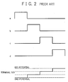
- Fig. 2 shows relationship between input control signals a, b, c and d supplied to the circuit shown 1 and potentials output from the input-output terminal 501.
- the control signals a, b, c and d are controlled so that one of these signals may be a high level.
- the control signal a is high
- the N-type MOSFET 517 is "ON" to output the ground signal from the input-output terminal 501.
- the control signal b is high
- both the P-type MOSFET 512 and N-type MOSFET 516 are “ON” to output the 1/3 VDD signal from the input-output terminal 501.
- the control signal c is high, both the P-type MOSFET 511 and N-type MOSFET 515 are “ON” to output the 2/3 VDD signal from the input-output terminal 501.
- the control signal d is high
- the P-type MOSFET 510 is "ON" to output the VDD signal from the input-output terminal 501.
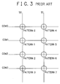
- a matrix type driver shown in Fig. 3 is used.
- Lines COM0 to COM3, S0 and S1 are inputs of the LCD and can be driven by the LCD drive terminal circuit shown in Fig. 1.
- Figs. 4A and 4B show display patterns of the LCD and are used for displaying numerals. For example, when displaying a numeral "1", patterns 1 and 2 are ON and the rest is OFF.
- the line S0 is connected to pattern 0 to pattern 3 and the line S1 to pattern 4 to pattern 7, as shown in Fig. 4A.
- the line COM0 is connected to pattern 0 and pattern 4, the line COM1 to pattern 1 and pattern 5, the line COM2 to pattern 2 and pattern 6, and the line COM3 to pattern 3 and pattern 7, as shown in Fig. 4B.
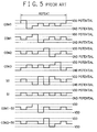
- a voltage amplitude is small between COM0 and S0 and between COM3 and S0, as shown by COM0-S0 and COM3-S0 in Fig. 6, and patterns 0 and 3 are OFF. Similarly, a voltage amplitude is small between COM0 to 3 and S1, and patterns 4 to 7 are OFF.
- Fig. 7 schematically shows one example of LCD drive terminals of the circuit shown in Fig. 1.
- the P-type MOSFET 514 and the N-type MOSFET 519 act as protective elements against electrostatic destruction.
- Fig. 8 shows the detailed layout and wiring of the LCD drive terminals shown in Fig. 7.
- a P-type diffusion layer 601 provides the source and the drain of the P-type MOSFET 514, and a polysilicon 604 provides the gate of the same.
- a second aluminum (A1) 607 is a wire for supplying a source potential to the source and the gate of the P-type MOSFET 514.
- An N-type diffusion layer 602 provides the source and the drain of the N-type MOSFET 519, and a polysilicon 603 provides the gate of the same.
- Another second aluminum 606 is a wire for supplying a ground potential to the source of the N-type MOSFET 519.
- a first aluminum 609 couples the drains of the P-type MOSFET 514 and the N-type MOSFET 519, the drains of the P-type MOSFETs 510 to 512 and the drains of the N-type MOSFETs 515 to 517 to a pad 541 corresponding to the input-output terminal 501.
- large size protective elements such as the N-type MOSFET 519 and the P-type MOSFET 514, as shown in Fig. 7, are mounted on the input-output terminal of the MOS type IC to diminish a current density caused when the static electricity is applied to the input-output terminal, resulting in preventing the destruction or breakdown.
- CMOS LSI An LSI using both a P-type MOSFET and an N-type MOSFET is called a CMOS LSI which involves a problem usually called "latch-up".
- This latch-up is a phenomenon of a current flow in a parasitic thyristor annexed to a CMOS structure and may bring about destruction of a chip at the worst.
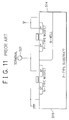
- Fig. 10 shows a parasitic thyristor.
- a parasitic thyristor of a PNPN structure is formed between an electric source and a ground.
- a latch-up is caused in this part, a large current flows between the electric source and the ground shown in Fig. 10.
- some P-type or N-type diffusion layer is connected to the input-output terminal 501.
- some P-type or N-type diffusion layer is connected to the input-output terminal 501.
- the PN junction between the drain of the N-type MOSFET 519 connected to the input-output terminal 501 and a P-type substrate coupled to the ground turns out to be a forward bias and a large current flows therein.
- a part of the large current flowing in the P-type substrate reaches a parasitic thyristor shown in Fig. 10, which is positioned near the terminal part of the CMOS type IC shown in Fig. 11.
- the P-type substrate provides the gate of the thyristor, and, when it is sufficient for the reached current to allow the thyristor to be conductive, the parasitic thyristor becomes conductive and turns to latch-up.
- the chip Since this latch-up brings about the destruction of the chip at the worst, the chip is designed so that the latch-up phenomenon may not happen as far as possible.
- the P-type and N-type diffusion layers connected directly to the input-output terminal are exactly separated from other P-type and N-type diffusion layers at a predetermined distance.
- the P-type and N-type diffusion layers connected directly to the input-output terminal can act as the escape paths for the current to cause the latch-up and hence prevent the sufficient current to reach the parasitic thyristor from causing its conductive state and latch-up.
- a predetermined distance is given between the N-type MOSFET 519 and the P-type MOSFET 514, and between the P-type MOSFET 514 and the P-type and N-type MOSFETs 510 to 513 and 515 to 517.
- the LCD In a semiconductor device for implementing the LCD drive function, usually, the LCD includes many display elements and thus the number of drive terminals also increases.
- a semiconductor device comprising an N-type MOSFET whose drain is connected to an external input-output terminal and whose gate and source are connected to a ground; a P-type MOSFET whose drain is connected to the external input-output terminal and whose gate and source are connected to an electric source; and at least one MOSFET whose source and drain are connected to neither the electric source nor the ground, arranged between the N-type MOSFET and the P-type MOSFET.
- At least one MOSFET connected to neither an electric source nor a ground is arranged between a first protective diffusion layer having a first conductivity type, connected to a terminal and a second protective diffusion layer having a second conductivity type different from the first conductivity type, connected to the terminal, and in particular, for example, in a semiconductor device such as an LCD drive terminal circuit, a chip size can be reduced without damaging resistances against electrostatic destruction and latch-up.
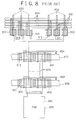
- FIG. 12 there is shown an improved layout of transistors near LCD drive terminals in a CMOS semiconductor device according to one embodiment of the present invention in Fig. 12.
- a used circuit is the same as the conventional one shown in Fig. 1.
- Fig. 12 schematically shows a layout of P-type MOSFETs 510 to 512 and 514 and N-type MOSFETs 515 to 517 and 519 connected to an input-output terminal 501, which are the same MOSFETs as those shown in Fig. 1.
- the P-type MOSFETs 511 and 512 whose sources are not directly connected to the electric source, and the N-type MOSFETs 515 and 516 whose sources are not directly coupled to the ground are arranged between the P-type MOSFET 514 and the N-type MOSFET 519.
- Fig. 13 shows a detailed layout of the MOSFETs shown in Fig. 12.
- a P-type diffusion layer 601 provides the source and the drain of the P-type MOSFET 514, and a polysilicon 604 provides the gate of the same.
- a second aluminum (A1) 607 is a wire for supplying a source potential to the source and the gate of the P-type MOSFET 514.
- An N-type diffusion layer 602 provides the source and the drain of the N-type MOSFET 519, and a polysilicon 603 provides the gate of the same.
- Another second aluminum 606 is a wire for supplying a ground potential to the source of the N-type MOSFET 519.
- a first aluminum 609 couples the drains of the P-type MOSFET 514 and the N-type MOSFET 519, the drains of the P-type MOSFETs 510 to 512 and the drains of the N-type MOSFETs 515 to 517 to a pad 541 corresponding to the input-output terminal 501.
- the P-type MOSFETs 511 and 512 and the N-type MOSFETs 515 and 516 are small-sized, and the drains of the P-type MOSFETs 511 and 512 and the drains of the N-type MOSFETs 515 and 516 have respective diffusion layers and contacts in common.
- the drive terminal circuit has the same construction as that of the conventional one shown in Fig. 1.
- the display operation of the LCD is the same as that of the conventional example described above and thus the description thereof can be omitted for brevity.
- the P-type MOSFET 514 and the N-type MOSFET 519 act as protective elements against electrostatic destruction in the same manner as those of the conventional example described above.
- latch-up can occur in the diffusion layers coupled to the input-output terminal.
- the P-type MOSFET 511 and the N-type MOSFET 519 are positioned close to each other and there is a possibility of occurrence of the latch-up.
- a resistor 520 is inserted on the source side of the P-type MOSFET 511.
- a high value resistor of approximately 100k ⁇ is used for a voltage-dividing resistor 520 shown in Fig. 1 in order to produce the required voltage for displaying the LCD.
- a thyristor shown in Fig. 14 cannot be changed to be conductive by applying a usual VDD voltage of approximately 5V. That is, in this embodiment, the possibility of the latch-up occurrence cannot be increased.
- the MOSFETs whose sources are not connected to the electric source nor the ground are arranged between the two protective diffusion layers having different polarities, to which the input-output terminal is coupled.
- the chip area of the semiconductor device can be effectively used and the production cost can be reduced.
- the chip size reduction and the cost reduction can be realized without damaging the resistance against the electrostatic destruction and the resistance against the latch-up.
Landscapes
- Engineering & Computer Science (AREA)
- Chemical & Material Sciences (AREA)
- Crystallography & Structural Chemistry (AREA)
- Physics & Mathematics (AREA)
- Computer Hardware Design (AREA)
- General Physics & Mathematics (AREA)
- Theoretical Computer Science (AREA)
- Metal-Oxide And Bipolar Metal-Oxide Semiconductor Integrated Circuits (AREA)
- Semiconductor Integrated Circuits (AREA)
Applications Claiming Priority (3)
| Application Number | Priority Date | Filing Date | Title |
|---|---|---|---|
| JP323623/95 | 1995-11-17 | ||
| JP7323623A JP2751898B2 (ja) | 1995-11-17 | 1995-11-17 | 半導体装置 |
| JP32362395 | 1995-11-17 |
Publications (2)
| Publication Number | Publication Date |
|---|---|
| EP0774786A2 true EP0774786A2 (de) | 1997-05-21 |
| EP0774786A3 EP0774786A3 (de) | 1999-11-03 |
Family
ID=18156809
Family Applications (1)
| Application Number | Title | Priority Date | Filing Date |
|---|---|---|---|
| EP96118200A Withdrawn EP0774786A3 (de) | 1995-11-17 | 1996-11-13 | CMOS-Halbleiter-Bauteil |
Country Status (4)
| Country | Link |
|---|---|
| US (1) | US5883415A (de) |
| EP (1) | EP0774786A3 (de) |
| JP (1) | JP2751898B2 (de) |
| KR (1) | KR100234860B1 (de) |
Cited By (1)
| Publication number | Priority date | Publication date | Assignee | Title |
|---|---|---|---|---|
| EP2182507A1 (de) * | 2008-10-28 | 2010-05-05 | Powertip Technology Corp. | Intelligente LCD-Vorrichtung mit Reihen- und Mehrfarben-Rückbeleuchtungsmodulation und Verfahren dafür |
Families Citing this family (3)
| Publication number | Priority date | Publication date | Assignee | Title |
|---|---|---|---|---|
| KR20000029449A (ko) * | 1997-05-23 | 2000-05-25 | 롤페스 요하네스 게라투스 알베르투스 | 측방향엠오에스트랜지스터소자 |
| US6724594B2 (en) * | 2000-12-20 | 2004-04-20 | National Semiconductor Corporation | Over voltage protection test multiplexer and methods of operating the same |
| TWI234425B (en) * | 2004-03-03 | 2005-06-11 | Toppoly Optoelectronics Corp | Electrostatic discharge protection method for display and device thereof |
Family Cites Families (6)
| Publication number | Priority date | Publication date | Assignee | Title |
|---|---|---|---|---|
| JPS6329964A (ja) * | 1986-07-23 | 1988-02-08 | Mitsubishi Electric Corp | 相補型金属酸化膜半導体集積回路装置 |
| KR920000635B1 (ko) * | 1987-01-28 | 1992-01-17 | 가부시키가이샤 도시바 | 반도체집적회로장치 |
| US4819047A (en) * | 1987-05-15 | 1989-04-04 | Advanced Micro Devices, Inc. | Protection system for CMOS integrated circuits |
| US5239197A (en) * | 1990-01-29 | 1993-08-24 | Matsushita Electronics Corporation | Non-volatile memory device and transistor circuits on the same chip |
| JPH0653497A (ja) * | 1991-08-23 | 1994-02-25 | Nec Corp | 入出力保護回路を備えた半導体装置 |
| JPH05150748A (ja) * | 1991-11-29 | 1993-06-18 | Fujitsu Ltd | 液晶表示装置及びその駆動回路のための基準電圧供給回路 |
-
1995
- 1995-11-17 JP JP7323623A patent/JP2751898B2/ja not_active Expired - Fee Related
-
1996
- 1996-11-13 EP EP96118200A patent/EP0774786A3/de not_active Withdrawn
- 1996-11-14 US US08/749,942 patent/US5883415A/en not_active Expired - Lifetime
- 1996-11-15 KR KR1019960055500A patent/KR100234860B1/ko not_active Expired - Fee Related
Non-Patent Citations (1)
| Title |
|---|
| None |
Cited By (1)
| Publication number | Priority date | Publication date | Assignee | Title |
|---|---|---|---|---|
| EP2182507A1 (de) * | 2008-10-28 | 2010-05-05 | Powertip Technology Corp. | Intelligente LCD-Vorrichtung mit Reihen- und Mehrfarben-Rückbeleuchtungsmodulation und Verfahren dafür |
Also Published As
| Publication number | Publication date |
|---|---|
| US5883415A (en) | 1999-03-16 |
| KR100234860B1 (ko) | 1999-12-15 |
| JPH09148451A (ja) | 1997-06-06 |
| EP0774786A3 (de) | 1999-11-03 |
| JP2751898B2 (ja) | 1998-05-18 |
| KR970030788A (ko) | 1997-06-26 |
Similar Documents
| Publication | Publication Date | Title |
|---|---|---|
| EP0172305B1 (de) | MOS-Transistorschaltung mit Durchschlagschutz | |
| US6696701B2 (en) | Electrostatic discharge protection for pixellated electronic device | |
| US6239958B1 (en) | Electrostatic damage protection circuit and dynamic random access memory | |
| JPH06163824A (ja) | 半導体集積回路 | |
| JPH0369141A (ja) | セミカスタム半導体集積回路 | |
| US6608744B1 (en) | SOI CMOS input protection circuit with open-drain configuration | |
| US5144518A (en) | Semiconductor integrated circuit | |
| JP2589938B2 (ja) | 半導体集積回路装置の静電破壊保護回路 | |
| US20030193765A1 (en) | Electrostatic breakdown prevention circuit for semiconductor device | |
| US4859878A (en) | Bi-MOS levelshift circuit capable of controlling power consumption | |
| US5883415A (en) | CMOS semiconductor device with improved layout of transistors near LCD drive terminals | |
| KR101009305B1 (ko) | 반도체 칩의 장변을 따라 연장된 정전기 보호 소자를 갖는반도체 디바이스 | |
| KR19980024056A (ko) | 반도체 집적 회로장치 | |
| KR20000045291A (ko) | 액정 표시 소자 | |
| JP3267479B2 (ja) | 半導体集積回路装置 | |
| KR100240131B1 (ko) | 씨엠오에스(cmos)회로의 래치업 저감출력드라이버 및 래치 업 저감방법 | |
| US6833590B2 (en) | Semiconductor device | |
| US6583475B2 (en) | Semiconductor device | |
| JP2003084304A (ja) | 液晶表示装置 | |
| JPH0410225B2 (de) | ||
| JPH11233778A (ja) | 表示装置 | |
| JPH1168038A (ja) | 半導体集積回路装置における静電破壊保護回路 | |
| JP3141511B2 (ja) | 信号入力回路およびアクティブマトリクスパネル | |
| KR0158626B1 (ko) | 전원단자의 정전기 보호회로 | |
| JP3369353B2 (ja) | 半導体装置の保護回路 |
Legal Events
| Date | Code | Title | Description |
|---|---|---|---|
| PUAI | Public reference made under article 153(3) epc to a published international application that has entered the european phase |
Free format text: ORIGINAL CODE: 0009012 |
|
| AK | Designated contracting states |
Kind code of ref document: A2 Designated state(s): DE FR GB |
|
| PUAL | Search report despatched |
Free format text: ORIGINAL CODE: 0009013 |
|
| AK | Designated contracting states |
Kind code of ref document: A3 Designated state(s): DE FR GB |
|
| 17P | Request for examination filed |
Effective date: 20000105 |
|
| STAA | Information on the status of an ep patent application or granted ep patent |
Free format text: STATUS: THE APPLICATION HAS BEEN WITHDRAWN |
|
| 18W | Application withdrawn |
Effective date: 20021220 |