EP0777211A2 - Lesekanal für eine Magnetplatte mit Amplitudenabtastung mit interpolierender Rückgewinnung des Zeittaktes zur synchronen Erfassung von eingebetteten Servodaten - Google Patents
Lesekanal für eine Magnetplatte mit Amplitudenabtastung mit interpolierender Rückgewinnung des Zeittaktes zur synchronen Erfassung von eingebetteten Servodaten Download PDFInfo
- Publication number
- EP0777211A2 EP0777211A2 EP96119296A EP96119296A EP0777211A2 EP 0777211 A2 EP0777211 A2 EP 0777211A2 EP 96119296 A EP96119296 A EP 96119296A EP 96119296 A EP96119296 A EP 96119296A EP 0777211 A2 EP0777211 A2 EP 0777211A2
- Authority
- EP
- European Patent Office
- Prior art keywords
- sample values
- data
- channel
- discrete time
- sampling
- Prior art date
- Legal status (The legal status is an assumption and is not a legal conclusion. Google has not performed a legal analysis and makes no representation as to the accuracy of the status listed.)
- Granted
Links
- 238000011084 recovery Methods 0.000 title claims abstract description 79
- 230000001360 synchronised effect Effects 0.000 title claims abstract description 49
- 230000005291 magnetic effect Effects 0.000 title claims abstract description 33
- 238000001514 detection method Methods 0.000 title description 45
- 238000005070 sampling Methods 0.000 claims abstract description 110
- 238000000034 method Methods 0.000 claims abstract description 40
- 230000004044 response Effects 0.000 abstract description 45
- 238000001228 spectrum Methods 0.000 abstract description 26
- 230000036961 partial effect Effects 0.000 abstract description 17
- 230000008569 process Effects 0.000 abstract description 11
- 239000011159 matrix material Substances 0.000 description 33
- 230000002829 reductive effect Effects 0.000 description 13
- 230000006870 function Effects 0.000 description 10
- 238000010586 diagram Methods 0.000 description 7
- 238000004891 communication Methods 0.000 description 5
- 238000007476 Maximum Likelihood Methods 0.000 description 4
- 230000007423 decrease Effects 0.000 description 4
- 230000003247 decreasing effect Effects 0.000 description 4
- 230000003044 adaptive effect Effects 0.000 description 3
- 230000008901 benefit Effects 0.000 description 3
- 238000013461 design Methods 0.000 description 3
- 230000000694 effects Effects 0.000 description 3
- 230000001052 transient effect Effects 0.000 description 3
- 238000000354 decomposition reaction Methods 0.000 description 2
- 230000007547 defect Effects 0.000 description 2
- 230000001934 delay Effects 0.000 description 2
- 230000004048 modification Effects 0.000 description 2
- 238000012986 modification Methods 0.000 description 2
- 238000012546 transfer Methods 0.000 description 2
- 230000007704 transition Effects 0.000 description 2
- VIFIHLXNOOCGLJ-UHFFFAOYSA-N trichloro(3,3,4,4,5,5,6,6,7,7,8,8,9,9,10,10,10-heptadecafluorodecyl)silane Chemical compound FC(F)(F)C(F)(F)C(F)(F)C(F)(F)C(F)(F)C(F)(F)C(F)(F)C(F)(F)CC[Si](Cl)(Cl)Cl VIFIHLXNOOCGLJ-UHFFFAOYSA-N 0.000 description 2
- 239000002023 wood Substances 0.000 description 2
- 101000606504 Drosophila melanogaster Tyrosine-protein kinase-like otk Proteins 0.000 description 1
- 101710162828 Flavin-dependent thymidylate synthase Proteins 0.000 description 1
- PEDCQBHIVMGVHV-UHFFFAOYSA-N Glycerine Chemical compound OCC(O)CO PEDCQBHIVMGVHV-UHFFFAOYSA-N 0.000 description 1
- 101710135409 Probable flavin-dependent thymidylate synthase Proteins 0.000 description 1
- 241001620634 Roger Species 0.000 description 1
- 230000001364 causal effect Effects 0.000 description 1
- 230000008859 change Effects 0.000 description 1
- 230000002950 deficient Effects 0.000 description 1
- 238000009795 derivation Methods 0.000 description 1
- 238000005516 engineering process Methods 0.000 description 1
- 230000004907 flux Effects 0.000 description 1
- 230000036039 immunity Effects 0.000 description 1
- 230000006872 improvement Effects 0.000 description 1
- 230000000873 masking effect Effects 0.000 description 1
- 238000012545 processing Methods 0.000 description 1
- 230000011664 signaling Effects 0.000 description 1
- 230000003068 static effect Effects 0.000 description 1
Images




Classifications
-
- H—ELECTRICITY
- H04—ELECTRIC COMMUNICATION TECHNIQUE
- H04L—TRANSMISSION OF DIGITAL INFORMATION, e.g. TELEGRAPHIC COMMUNICATION
- H04L7/00—Arrangements for synchronising receiver with transmitter
- H04L7/0016—Arrangements for synchronising receiver with transmitter correction of synchronization errors
- H04L7/002—Arrangements for synchronising receiver with transmitter correction of synchronization errors correction by interpolation
- H04L7/0029—Arrangements for synchronising receiver with transmitter correction of synchronization errors correction by interpolation interpolation of received data signal
-
- G—PHYSICS
- G11—INFORMATION STORAGE
- G11B—INFORMATION STORAGE BASED ON RELATIVE MOVEMENT BETWEEN RECORD CARRIER AND TRANSDUCER
- G11B20/00—Signal processing not specific to the method of recording or reproducing; Circuits therefor
- G11B20/10—Digital recording or reproducing
- G11B20/10009—Improvement or modification of read or write signals
-
- G—PHYSICS
- G11—INFORMATION STORAGE
- G11B—INFORMATION STORAGE BASED ON RELATIVE MOVEMENT BETWEEN RECORD CARRIER AND TRANSDUCER
- G11B20/00—Signal processing not specific to the method of recording or reproducing; Circuits therefor
- G11B20/10—Digital recording or reproducing
- G11B20/10009—Improvement or modification of read or write signals
- G11B20/10037—A/D conversion, D/A conversion, sampling, slicing and digital quantisation or adjusting parameters thereof
-
- G—PHYSICS
- G11—INFORMATION STORAGE
- G11B—INFORMATION STORAGE BASED ON RELATIVE MOVEMENT BETWEEN RECORD CARRIER AND TRANSDUCER
- G11B20/00—Signal processing not specific to the method of recording or reproducing; Circuits therefor
- G11B20/10—Digital recording or reproducing
- G11B20/10009—Improvement or modification of read or write signals
- G11B20/10046—Improvement or modification of read or write signals filtering or equalising, e.g. setting the tap weights of an FIR filter
- G11B20/10055—Improvement or modification of read or write signals filtering or equalising, e.g. setting the tap weights of an FIR filter using partial response filtering when writing the signal to the medium or reading it therefrom
-
- G—PHYSICS
- G11—INFORMATION STORAGE
- G11B—INFORMATION STORAGE BASED ON RELATIVE MOVEMENT BETWEEN RECORD CARRIER AND TRANSDUCER
- G11B20/00—Signal processing not specific to the method of recording or reproducing; Circuits therefor
- G11B20/10—Digital recording or reproducing
- G11B20/10009—Improvement or modification of read or write signals
- G11B20/10046—Improvement or modification of read or write signals filtering or equalising, e.g. setting the tap weights of an FIR filter
- G11B20/10055—Improvement or modification of read or write signals filtering or equalising, e.g. setting the tap weights of an FIR filter using partial response filtering when writing the signal to the medium or reading it therefrom
- G11B20/10064—EEPR4 or E2PR4, i.e. extended partial response class 4, polynomial (1-D)*(1+D)3
-
- G—PHYSICS
- G11—INFORMATION STORAGE
- G11B—INFORMATION STORAGE BASED ON RELATIVE MOVEMENT BETWEEN RECORD CARRIER AND TRANSDUCER
- G11B20/00—Signal processing not specific to the method of recording or reproducing; Circuits therefor
- G11B20/10—Digital recording or reproducing
- G11B20/10009—Improvement or modification of read or write signals
- G11B20/10046—Improvement or modification of read or write signals filtering or equalising, e.g. setting the tap weights of an FIR filter
- G11B20/10055—Improvement or modification of read or write signals filtering or equalising, e.g. setting the tap weights of an FIR filter using partial response filtering when writing the signal to the medium or reading it therefrom
- G11B20/10074—EPR4, i.e. extended partial response class 4, polynomial (1-D) *(1+D)2
-
- G—PHYSICS
- G11—INFORMATION STORAGE
- G11B—INFORMATION STORAGE BASED ON RELATIVE MOVEMENT BETWEEN RECORD CARRIER AND TRANSDUCER
- G11B20/00—Signal processing not specific to the method of recording or reproducing; Circuits therefor
- G11B20/10—Digital recording or reproducing
- G11B20/14—Digital recording or reproducing using self-clocking codes
- G11B20/1403—Digital recording or reproducing using self-clocking codes characterised by the use of two levels
-
- G—PHYSICS
- G11—INFORMATION STORAGE
- G11B—INFORMATION STORAGE BASED ON RELATIVE MOVEMENT BETWEEN RECORD CARRIER AND TRANSDUCER
- G11B5/00—Recording by magnetisation or demagnetisation of a record carrier; Reproducing by magnetic means; Record carriers therefor
- G11B5/02—Recording, reproducing, or erasing methods; Read, write or erase circuits therefor
- G11B5/09—Digital recording
-
- H—ELECTRICITY
- H04—ELECTRIC COMMUNICATION TECHNIQUE
- H04L—TRANSMISSION OF DIGITAL INFORMATION, e.g. TELEGRAPHIC COMMUNICATION
- H04L7/00—Arrangements for synchronising receiver with transmitter
- H04L7/0054—Detection of the synchronisation error by features other than the received signal transition
- H04L7/0062—Detection of the synchronisation error by features other than the received signal transition detection of error based on data decision error, e.g. Mueller type detection
-
- G—PHYSICS
- G11—INFORMATION STORAGE
- G11B—INFORMATION STORAGE BASED ON RELATIVE MOVEMENT BETWEEN RECORD CARRIER AND TRANSDUCER
- G11B20/00—Signal processing not specific to the method of recording or reproducing; Circuits therefor
- G11B20/10—Digital recording or reproducing
- G11B20/12—Formatting, e.g. arrangement of data block or words on the record carriers
- G11B20/1217—Formatting, e.g. arrangement of data block or words on the record carriers on discs
- G11B20/1258—Formatting, e.g. arrangement of data block or words on the record carriers on discs where blocks are arranged within multiple radial zones, e.g. Zone Bit Recording or Constant Density Recording discs, MCAV discs, MCLV discs
-
- G—PHYSICS
- G11—INFORMATION STORAGE
- G11B—INFORMATION STORAGE BASED ON RELATIVE MOVEMENT BETWEEN RECORD CARRIER AND TRANSDUCER
- G11B20/00—Signal processing not specific to the method of recording or reproducing; Circuits therefor
- G11B20/10—Digital recording or reproducing
- G11B2020/1087—Digital recording or reproducing wherein a selection is made among at least two alternative ways of processing
- G11B2020/10888—Digital recording or reproducing wherein a selection is made among at least two alternative ways of processing the kind of data being the selection criterion
-
- G—PHYSICS
- G11—INFORMATION STORAGE
- G11B—INFORMATION STORAGE BASED ON RELATIVE MOVEMENT BETWEEN RECORD CARRIER AND TRANSDUCER
- G11B20/00—Signal processing not specific to the method of recording or reproducing; Circuits therefor
- G11B20/10—Digital recording or reproducing
- G11B20/12—Formatting, e.g. arrangement of data block or words on the record carriers
- G11B20/1217—Formatting, e.g. arrangement of data block or words on the record carriers on discs
- G11B2020/1218—Formatting, e.g. arrangement of data block or words on the record carriers on discs wherein the formatting concerns a specific area of the disc
- G11B2020/1232—Formatting, e.g. arrangement of data block or words on the record carriers on discs wherein the formatting concerns a specific area of the disc sector, i.e. the minimal addressable physical data unit
- G11B2020/1234—Formatting, e.g. arrangement of data block or words on the record carriers on discs wherein the formatting concerns a specific area of the disc sector, i.e. the minimal addressable physical data unit wherein the sector is a headerless sector, i.e. it does not comprise an ID field
-
- G—PHYSICS
- G11—INFORMATION STORAGE
- G11B—INFORMATION STORAGE BASED ON RELATIVE MOVEMENT BETWEEN RECORD CARRIER AND TRANSDUCER
- G11B20/00—Signal processing not specific to the method of recording or reproducing; Circuits therefor
- G11B20/10—Digital recording or reproducing
- G11B20/12—Formatting, e.g. arrangement of data block or words on the record carriers
- G11B2020/1264—Formatting, e.g. arrangement of data block or words on the record carriers wherein the formatting concerns a specific kind of data
- G11B2020/1265—Control data, system data or management information, i.e. data used to access or process user data
- G11B2020/1281—Servo information
- G11B2020/1282—Servo information in embedded servo fields
-
- H—ELECTRICITY
- H04—ELECTRIC COMMUNICATION TECHNIQUE
- H04L—TRANSMISSION OF DIGITAL INFORMATION, e.g. TELEGRAPHIC COMMUNICATION
- H04L7/00—Arrangements for synchronising receiver with transmitter
- H04L7/04—Speed or phase control by synchronisation signals
- H04L7/041—Speed or phase control by synchronisation signals using special codes as synchronising signal
- H04L2007/047—Speed or phase control by synchronisation signals using special codes as synchronising signal using a sine signal or unmodulated carrier
-
- H—ELECTRICITY
- H04—ELECTRIC COMMUNICATION TECHNIQUE
- H04L—TRANSMISSION OF DIGITAL INFORMATION, e.g. TELEGRAPHIC COMMUNICATION
- H04L7/00—Arrangements for synchronising receiver with transmitter
- H04L7/0004—Initialisation of the receiver
Definitions
- the present invention relates to the control of magnetic disk storage systems for digital computers, particularly to a sampled amplitude read channel that employs interpolated timing recovery for synchronous detection of embedded servo data.
- digital data serves to modulate the current in a read/write head coil in order to write a sequence of corresponding magnetic flux transitions onto the surface of a magnetic medium in concentric, radially spaced tracks at a predetermined baud rate.
- the read/write head again passes over the magnetic medium and transduces the magnetic transitions into pulses in an analog signal that alternate in polarity. These pulses are then decoded by read channel circuitry to reproduce the digital data.
- Decoding the pulses into a digital sequence can be performed by a simple peak detector in a conventional analog read channel or, as in more recent designs, by a discrete time sequence detector in a sampled amplitude read channel.
- Discrete time sequence detectors are preferred over simple analog pulse detectors because they compensate for intersymbol interference (ISI) and are less susceptible to channel noise. As a result, discrete time sequence detectors increase the capacity and reliability of the storage system.
- ISI intersymbol interference
- DPD discrete time pulse detection
- PR partial response
- MLSD maximum likelihood sequence detection
- DFE decision-feedback equalization
- EDFE enhanced decision-feedback equalization
- FDTS/DF fixed-delay tree-search with decision-feedback
- analog circuitry responsive to threshold crossing or derivative information, detects peaks in the continuous time analog signal generated by the read head.
- the analog read signal is "segmented” into bit cell periods and interpreted during these segments of time. The presence of a peak during the bit cell period is detected as a "1" bit, whereas the absence of a peak is detected as a "0" bit.
- Timing recovery then, adjusts the bit cell periods so that the peaks occur in the center of the bit cells on average in order to minimize detection errors. Since timing information is derived only when peaks are detected, the input data stream is normally run length limited (RLL) to limit the number of consecutive "0" bits.
- RLL run length limited
- detection errors can also occur due to intersymbol interference, a distortion in the read signal caused by closely spaced overlapping pulses. This interference can cause a peak to shift out of its bit cell, or its magnitude to decrease, resulting in a detection error.
- the ISI effect is reduced by decreasing the data density or by employing an encoding scheme that ensures a minimum number of "0" bits occur between "1" bits.
- a (d,k) run length limited (RLL) code constrains to d the minimum number of "0" bits between "1” bits, and to k the maximum number of consecutive "0" bits.
- RLL 2/3 rate code encodes 8 bit data words into 12 bit codewords to satisfy the (1,7) constraint.
- Sampled amplitude detection such as partial response (PR) with Viterbi detection, allows for increased data density by compensating for intersymbol interference and the effect of channel noise.
- sampled amplitude recording detects digital data by interpreting, at discrete time instances, the actual value of the pulse data.
- the read channel comprises a sampling device for sampling the analog read signal, and a timing recovery circuit for synchronizing the samples to the baud rate (code bit rate).
- a low pass analog filter processes the read signal to attenuate aliasing noise.
- a digital equalizing filter After sampling, a digital equalizing filter equalizes the sample values according to a desired partial response, and a discrete time sequence detector, such as a Viterbi detector, interprets the equalized sample values in context to determine a most likely sequence for the digital data (i.e., maximum likelihood sequence detection MLSD).
- a discrete time sequence detector such as a Viterbi detector interprets the equalized sample values in context to determine a most likely sequence for the digital data (i.e., maximum likelihood sequence detection MLSD).
- a sampled amplitude read channel can take into account the effect of ISI and channel noise during the detection process, thereby decreasing the probability of a detection error. This increases the effective signal to noise ratio and, for a given (d,k) constraint, allows for significantly higher data density as compared to conventional analog peak detection read channels.
- sampled amplitude detection requires timing recovery in order to correctly extract the digital sequence. Rather than process the continuous signal to align peaks to the center of bit cell periods as in peak detection systems, sampled amplitude systems synchronize the pulse samples to the baud rate. In prior art sampled amplitude read channels, timing recovery synchronizes a sampling clock by minimizing an error between the signal sample values and estimated sample values. A pulse detector or slicer determines the estimated sample values from the read signal samples. Even in the presence of ISI the sample values can be estimated and, together with the signal sample values, used to synchronize the sampling of the analog pulses in a decision-directed feedback system.
- a phase-locked-loop normally implements the decision-directed feedback system to control timing recovery in sampled amplitude read channels.
- the PLL comprises a phase detector which generates a phase error based on the difference between the estimated samples and the read signal samples.
- a loop filter in the PLL filters the phase error, and the filtered phase error operates to synchronize the channel samples to the baud rate.
- the phase error adjusts the frequency of a sampling clock which is typically the output of a variable frequency oscillator (VFO).
- VFO variable frequency oscillator
- the output of the VFO controls a sampling device, such as an analog-to-digital (A/D) converter, to synchronize the pulse samples to the baud rate.
- A/D analog-to-digital
- the PLL input switches from the write clock to the signal from the read head in order to synchronize the sampling of the waveform in response to a sinusoidal acquisition preamble recorded on the medium.
- FIG. 2A shows a magnetic disk comprising a plurality of concentric data tracks 13 wherein each data track 13 comprises a plurality of sectors 15 .
- Servo data in the form of wedges 17 are embedded into the sectors 15 and used to control and verify the track and sector position of the read/write head.
- Figure 2B shows the format of a sector 15 comprising an acquisition preamble 68 , a sync mark 70 , and user data 72 .
- the acquisition preamble is a predetermined sequence that allows timing recovery to acquire the desired sampling phase and frequency before reading the user data.
- the PLL switches to a tracking mode in order to track the desired sampling phase and frequency with respect to the analog pulses representing the user data.
- the sync mark signals the beginning of the user data.
- a short acquisition preamble is desirable to allow more storage area for user data.
- Zoned recording is a technique known in the art for increasing the storage density by recording the user data at different rates in predefined zones between the inner diameter and outer diameter tracks.
- the data rate can be increased at the outer diameter tracks due to the increase in circumferential recording area and the decrease in intersymbol interference. This allows more data to be stored in the outer diameter tracks as is illustrated in Figure 2A where the disk is partitioned into an outer zone 11 comprising fourteen data sectors per track, and an inner zone 27 comprising seven data sectors per track.
- the disk may actually be partitioned into several zones at varying data rates.
- U.S. Pat. No. 5,359,631 entitled "Timing Recovery Circuit for Synchronous Waveform Sampling” discloses yet another method for timing recovery in a sampled amplitude read channel.
- a stochastic gradient circuit uses the estimated sample values, together with the signal sample values, to generate the phase error for adjusting the sampling clock in the decision-directed feedback system.
- the timing recovery loop filter controls the dynamics of the decision-directed feedback system. Accordingly, the loop filter coefficients are adjusted to achieve a desired transient response and tracking quality.
- the loop bandwidth should be narrow in order to attenuat phase noise and gain variance.
- the loop bandwidth should be as wide as possible without being unstable to achieve a fast transient response. A fast transient response results in a shorter acquisition time which minimizes the necessary length of the acquisition preamble.
- the phase error operates to adjust the sampling rate of the sampling VFO relative to the data rate of a particular zone on the disk. That is, when the read head passes into a new zone (e.g., outer zone 11 to inner zone 27 of Figure 2A), the frequency of the sampling VFO is adjusted and eventually synchronized to the data rate of the new zone. This is normally accomplished by programming a center frequency setting of the sampling VFO to a value corresponding to the new zone, and then adjusting a fine frequency setting until the sampling VFO is synchronized to the data rate.
- a new zone e.g., outer zone 11 to inner zone 27 of Figure 2A
- the slight difference in operating frequencies between the write VFO and the sampling VFO can result in cross-talk that degrades the performance of timing recovery.
- adjusting the sampling rate relative to a particular zone requires a programmable analog filter to compensate for aliasing at the various data rates, a complex and expensive implementation that requires calibrating the analog filter to operate in each zone.
- a further object is to avoid using a separate servo VFO for synchronous detection of embedded servo data.
- Still another object is to obviate the expensive, programmable analog filter used for anti-aliasing in prior art zoned recording read channels.
- Yet another object is to remove the sampling device and discrete time equalizing filter, and their associated latencies, from the timing recovery loop.
- a sampled amplitude read channel for magnetic disk recording ansynchronously sampling the analog read signal at a fixed sample rate across the entire disk (i.e., a fixed sample rate over the various user data zones and the embedded servo wedges), extracting synchronous samples from the asynchronous samples using interpolated timing recovery rather than sampled timing recovery, and detecting the recorded digital data from the interpolated sample values.
- a write synthesizer generates a write clock for writing digital data to the magnetic disk at a predetermined baud rate for a selected zone, and upon read back, a read synthesizer generates a fixed sampling clock at a frequency slightly higher than the write frequency at the outer diameter zone (i.e, slightly higher than the highest baud rate).
- a sampling device samples the analog read signal at this fixed sample rate across the various data zones and servo wedges to generate a sequence of discrete time channel samples that are not synchronized to the baud rate.
- an analog receive filter having a fixed frequency response attenuates aliasing noise.
- an equalizing filter equalizes the asynchronous channel samples according to a predetermined partial response (e.g., PR4, EPR4, EEPR4, DFE, etc.).
- An interpolating timing recovery circuit responsive to the equalized channel samples, computes an interpolation interval ⁇ and, in response thereto, generates interpolated sample values substantially synchronized to the baud rate.
- the interpolated timing recovery circuit also generates a data clock for clocking a discrete time sequence detector and a discrete time peak detector for detecting the user and servo data from the interpolated sample values.
- the interpolating timing recovery does not use a separate sampling VFO, cross talk between the write VFO is avoided. Further, a separate servo VFO is not needed for synchronous detection of embedded servo data because the interpolating timing recovery can be adjusted on-the-fly to the servo data rate.
- the analog anti-aliasing filter can be fixed, rather than programmable, since the sampling rate is fixed over the entire disk. Still further, the sampling device and discrete time equalizing filter have been removed from the timing recovery loop, thereby avoiding the associated latencies.
- FIG. 1 shown is a detailed block diagram of a conventional sampled amplitude read channel.
- a data generator 4 for example 2T preamble data
- An RLL encoder 6 encodes the user data 2 into a binary sequence b(n) 8 according to an RLL constraint.
- a precoder 10 precodes the binary sequence b(n) 8 in order to compensate for the transfer function of the recording channel 18 and equalizing filters to form a precoded sequence ⁇ b(n) 12 .
- Write circuitry 9 responsive to the symbols a(n) 16 , modulates the current in the recording head coil at the baud rate 1/T to record the binary sequence onto the media.
- a frequency synthesizer 52 provides a baud rate write clock 54 to the write circuitry 9 and is adjusted by a channel data rate signal (CDR) 30 according to the zone the write head is over.
- CDR channel data rate signal
- timing recovery 28 When reading the recorded binary sequence from the media, timing recovery 28 first locks to the write frequency by selecting, as the input to the read channel, the write clock 54 through a multiplexor 60 . Once locked to the write frequency, the multiplexor 60 selects the signal 19 from the read head as the input to the read channel in order to acquire an acquisition preamble.
- a variable gain amplifier 22 adjusts the amplitude of the analog read signal 58 , and an analog filter 20 provides initial equalization toward the desired response as well as attenuating aliasing noise.
- a sampling device 24 samples the analog read signal 62 from the analog filter 20 , and a discrete time filter 26 provides further equalization of the sample values 25 toward the desired response. In partial response recording, for example, the desired response is often selected from Table 1.
- the equalized sample values 32 are applied to decision directed gain control 50 and timing recovery 28 for adjusting the amplitude of the read signal 58 and the frequency and phase of the sampling device 24 , respectively.
- Timing recovery adjusts the frequency of sampling device 24 over line 23 in order to synchronize the equalized samples 32 to the baud rate.
- Frequency synthesizer 52 provides a course center frequency setting to the timing recovery circuit 28 over line 64 in order to center the timing recovery frequency over temperature, voltage, and process variations.
- the channel data rate (CDR) 30 signal adjusts a frequency range of the synthesizer 52 according to the data rate for the current zone.
- Gain control 50 adjusts the gain of variable gain amplifier 22 over line 21 .
- the equalized samples Y(n) 32 are sent to a discrete time sequence detector 34 , such as a maximum likelihood (ML) Viterbi sequence detector, and to a discrete time peak detector 70 which detect an estimated binary sequence of user/servo data.
- An RLL decoder 36 decodes the estimated binary sequence ⁇ b(n) 33 from the sequence detector 34 into estimated user/servo data 37 .
- a data sync detector 66 detects the sync mark 70 (shown in Figure 2B) in the data sector 15 in order to frame the operation of the RLL decoder 36 .
- a multiplexor 72 selects the output 37 of the RLL decoder 36 or peak detector 70 as the estimated decoded servo data 74 output to a servo controller (not shown) for positioning the read/write head.
- the estimated binary sequence ⁇ b(n) 33 equals the recorded binary sequence b(n) 8
- the decoded user data 37 equals the recorded user data 2 .
- Figure 2A shows an exemplary data format of a magnetic media comprising a series of concentric data tracks 13 wherein each data track 13 comprises a plurality of sectors 15 with embedded servo wedges 17 .
- a servo controller (not shown) processes the servo data in the servo wedges 17 and, in response thereto, positions the read/write head over a desired track. Additionally, the servo controller processes servo bursts within the servo wedges 17 to keep the head aligned over a centerline of the desired track while writing and reading data.
- the servo wedges 17 may be detected by a simple discrete time pulse detector 70 or by the discrete time sequence detector 34 . If the sequence detector 34 detects the servo data, then the format of the servo wedges 17 includes a preamble and a sync mark, similar to the user data sectors 15 .
- Figure 2B shows the format of a user data sector 15 comprising an acquisition preamble 68 , a sync mark 70 , and user data 72 .
- Timing recovery uses the acquisition preamble 68 to acquire the correct sampling frequency and phase before reading the user data 72
- the sync mark 70 demarks the beginning of the user data 72 (see co-pending U.S. patent application 08/313,491 entitled "Improved Timing Recovery For Synchronous Partial Response Recording").
- the disk is partitioned into an outer zone 11 comprising fourteen data sectors per track, and an inner zone 27 comprising seven data sectors per track.
- the disk is actually partitioned into several zones and the data recorded and detected at varying data rates.
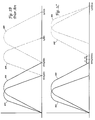
- Figure 1B shows a frequency spectrum of the sampled channel data according to the prior art method of adjusting the sampling rate relative to the data rate of the zone where the read head is positioned.
- Figure 1B shows the frequency spectrum of the channel when sampling at an outer diameter (OD) zone f s (OD) and at an inner diameter (ID) zone f s (ID).
- the analog receive filter 20 When sampling at f s (OD), the analog receive filter 20 must be programmed to pass frequencies 80A below 1/2 ⁇ f s (OD), and cutoff frequencies 80B higher than 1/2 ⁇ f s (OD).
- the analog receive filter 20 when sampling at f s (ID), the analog receive filter 20 must be programmed to pass frequencies 82A below 1/2 ⁇ f s (ID), and cutoff frequencies 82B higher than 1/2 ⁇ f s (ID).
- Programmable analog filters are expensive, complex in implementation, and must be calibrated to operate in each zone.
- the analog filter must have a relatively sharp rolloff so that it does not attenuate the signal spectrum below 1/2 ⁇ f s , which further increases its cost and complexity.
- the present invention reduces the complexity and cost of the analog filter by sampling 24 the analog read signal 19 at a fixed frequency across the entire disk. In this manner, the analog receive filter's cutoff frequency can remain fixed, and it does not require as sharp a rolloff.
- Figure 1C where the analog read signal 19 is sampled 24 at a frequency slightly higher than the data rate of the outer diameter track (i.e., sampled at f s (OD)+ ⁇ ).
- the analog receive filter 20 must pass frequencies below 1/2 ⁇ f s (OD) and cutoff frequencies above (1/2 ⁇ f s (OD))+2 ⁇ .
- the analog receive filter's cutoff frequency can remain fixed because the desired signal spectrum changes shape from the outer diameter (i.e., spectrum 84A ) to the inner diameter (i.e., spectrum 86A ), but the position of the aliased spectrums (i.e., spectrums 84B and 86B , respectively) remain fixed.
- the analog receive filter's rolloff can be flatter due to oversampling rather than synchronous sampling the read signal; that is, the analog filter's rolloff constraint lessens the more the read signal is oversampled (by increasing ⁇ ).
- Sampling the analog read signal at a fixed, oversampled rate requires two enabling modifications to the prior art sampled amplitude read channels: first, it requires interpolated (rather than synchronous sampling) timing recovery to extract synchronous data from the asynchronous samples; and second, it requires a more complex discrete time equalizing filter.
- the spectrum of the discrete time equalizing filter in prior art synchronous sampling read channels scales with the changing sampling rates across the zones. Only minor adjustments are necessary to compensate for any deviations in the disk's frequency response from zone to zone. In the present invention, however, the sampling rate is fixed across the zones; the spectrum of the discrete filter does not scale to the data rate ⁇ it must be adjusted accordingly. Accurate adjustment of the discrete filter's spectrum to generate the desired partial response across the various zones when using a fixed sampling rate requires a higher number of taps and coefficients.
- the discrete filter is normally implemented as a transversal FIR filter, and those skilled in the art can readily construct this filter with a sufficient number of taps and coefficients necessary to implement the fixed sampling technique of the present invention. The details of the discrete filter are, therefore, not included in this disclosure.
- the discrete time equalizing filter of the present invention requires more taps and coefficients in order to accurately shape the read signal's frequency response across the zones, the cost of discrete time circuitry, such as digital circuitry implemented in CMOS, is rapidly decreasing as the size and cost per gate decrease. In addition, digital circuitry is more robust and provides higher yields (i.e., less defective parts).
- the present invention provides yet another advantage in fixing the analog receive filter across the zones and loosening the rolloff constraint: it significantly reduces the cost and complexity of the analog filter. In fact, a simple, passive RC network will suffice.
- Figure B3 shows the improved sampled amplitude read channel of the present invention wherein the conventional sampled timing recovery 28 of Figure 1 has been replaced by interpolated timing recovery B100 .
- a write frequency synthesizer 52 for generating a baud rate write clock 54 applied to the write circuitry 9 at a frequency relative to the current zone (CDR 30 ) a read frequency synthesizer 53 generates a fixed sampling clock 55 applied to the sampling device 24 , the discrete time equalizer filter 26 , and the interpolated timing recovery B100 .
- the read frequency synthesizer 53 When reading data from any particular zone, the read frequency synthesizer 53 outputs a fixed sampling clock 55 at a frequency slightly higher than the highest data rate (which normally occurs at the outer diameter zone).
- the analog receive filter 20 used for anti-aliasing has a fixed spectrum since the sampling frequency does not change across the zones. This reduces the complexity and cost of the analog filter 20 and simplifies the operation of the read channel by not having to calibrate the analog filter 20 to operate optimumly in each zone.
- the interpolated timing recovery B100 interpolates the equalized sample values 32 to generate interpolated sample values B102 substantially synchronized to the data rate of the current zone or to the data rate of the servo wedge 17 .
- a discrete time sequence detector 34 detects an estimated binary sequence 33 representing the user/servo data from the interpolated sample values B102 .
- a discrete time pulse detector 70 detects the servo data from the interpolated sample values B102 .
- Interpolated timing recovery B100 generates a synchronous data clock B104 for clocking operation of the discrete time sequence detector 34 , discrete time pulse detector 70 , sync mark detector 66 and RLL decoder 36 .
- FIG. B4A An overview of the conventional sampling timing recovery 28 of Figure 1 is shown in Figure B4A.
- the output 23 of a variable frequency oscillator (VFO) B164 controls the sampling clock of a sampling device 24 which is typically an analog-to-digital converter (A/D) in digital read channels.
- a multiplexor B159 selects the unequalized sample values 25 during acquisition and the equalized sample values 32 during tracking, thereby removing the discrete equalizer filter 26 from the timing loop during acquisition in order to avoid its associated latency.
- a loop filter B160 filters the phase error to generate a frequency offset ⁇ B167 that settles to a value proportional to a frequency difference between the sampling clock 23 and the baud rate.
- the frequency offset ⁇ B167 together with the center frequency control signal 64 from the frequency synthesizer 52 , adjust the sampling clock 23 at the output of the VFO B164 in order to synchronize the sampling to the baud rate.
- a zero phase start B162 circuit suspends operation of the VFO 164 at the beginning of acquisition in order to minimize the initial phase error between the sampling clock 23 and the read signal 62 . This is achieved by disabling the VFO B164 , detecting a zero crossing in the analog read signal 62 , and re-enabling the VFO 164 after a predetermined delay between the detected zero crossing and the first baud rate sample.
- the interpolated timing recovery B100 of the present invention is shown in Figure B4B.
- the VFO B164 of Figure B4A is replaced with a modulo-Ts accumulator B120 and an interpolator B122 .
- an expected sample value generator B151 responsive to interpolated sample values B102 , generates expected samples X(n) used by the phase error detector 155 to compute the phase error during acquisition.
- a multiplexor B153 selects the estimated sample values ⁇ X(n) from the slicer for use by the phase error detector 155 during tracking.
- the data clock B104 is generated at the output of an AND gate B126 in response to the sampling clock 54 and a mask signal B124 from the modulo-Ts accumulator B120 as discussed in further detail below.
- phase error detector B155 and the slicer B141 process interpolated sample values B102 at the output of the interpolator B122 rather than the channel sample values 32 at the output of the discrete equalizer filter 26 as in Figure B4A.
- a PID loop filter B161 controls the closed loop frequency response similar to the loop filter B160 of Figure B4A.
- a zero phase start circuit B163 minimizes the initial phase error between the interpolated sample values and the baud rate at the beginning of acquisition similar to the zero phase start circuit B162 of Figure B4A.
- the zero phase start circuit B163 for interpolated timing recovery computes an initial phase error ⁇ from the equalized sample values 32 and loads the initial phase error into the modulo-Ts accumulator B120 .
- the interpolator B122 of Figure B4B is understood with reference to Figure B5 which shows a sampled 2T acquisition preamble signal B200 .
- the target synchronous sample values are shown as black circles and the asynchronous channel sample values as arrows.
- Bellow the sampled preamble signal is a timing diagram depicting the corresponding timing signals for the sampling clock 54 , the data clock B104 and the mask signal B124 .
- the preamble signal B200 is sampled slightly faster than the baud rate (the rate of the target values).
- the function of the interpolator is to estimate the target sample value by interpolating the channel sample values.
- channel sample values B202 and B204 are used to generate the interpolated sample value corresponding to target sample value B206 .
- the interpolation interval ⁇ B208 is generated according to equation (2) above.
- the next interpolated sample value corresponding to the next target value B210 is computed from channel sample values B204 and B212 .
- This process continues until the interpolation interval ⁇ B214 would be greater than Ts except that it "wraps" around and is actually ⁇ B216 (i.e., the accumulated frequency offset ⁇ , integer divided by Ts, increments by 1 causing the mask signal B124 to activate).
- the data clock B104 is masked by mask signal B124 so that the interpolated sample value corresponding to the target sample value B220 is computed from channel sample values B222 and B224 rather than channel sample values B218 and B222 .
- the interpolator B122 is implemented as a filter responsive to more than two channel samples to compute the interpolated sample value.
- the above non-causal infinite impulse response (4) cannot be realized. Therefore, the impulse response of the interpolation filter is designed to be a best fit approximation of the ideal impulse response (4). This can be accomplished by minimizing a mean squared error between the frequency response of the actual interpolation filter and the frequency response of the ideal interpolation filter (3).
- X( e j ⁇ ) is the spectrum of the read channel (e.g., PR4, EPR4, EEPR4 of Table 1 or some other partial response spectrum).
- equation (6) is modified by specifying that the spectrum of the input signal is bandlimitted to some predetermined constant 0 ⁇ ⁇ ⁇ ⁇ where 0 ⁇ ⁇ ⁇ 1; that is:
- 0, for
- the solution to the minimization problem of equation (7) involves expressing the actual interpolation filter in terms of its coefficients and then solving for the coefficients that minimize the error in a classical mean-square sense.
- a mathematical derivation for an interpolation filter having an even number of coefficients is provided bellow. It is within the ability of those skilled in the art to modify the mathematics to derive an interpolation filter having an odd number of coefficients.
- Equation (13) defines a set of 2R linear equations in terms of the coefficients C ⁇ (n).
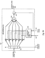
- the implementation of the six tap FIR filter is shown in Figure B6.
- a shift register B250 receives the channel samples 32 at the sampling clock rate 54 .
- the filter coefficients C ⁇ (n) are stored in a coefficient register file B252 and applied to corresponding multipliers according to the current value of ⁇ B128 .
- the coefficients are multiplied by the channel samples 32 stored in the shift register B250 .
- the resulting products are summed B254 and the sum stored in a delay register B256 .
- the coefficient register file B252 and the delay register B256 are clocked by the data clock B104 to implement the masking function described above.
- a plurality of static FIR filters having coefficients that correspond to the different values of ⁇ , filter the sample values in the shift register B250 .
- Each filter outputs an interpolation value, and the current value of the interpolation interval ⁇ B128 selects the output of the corresponding filter as the output B102 of the interpolator B122 . Since the coefficients of one filter are not constantly updated as in Figure B6, this multiple filter embodiment increases the speed of the interpolator B122 and the overall throughput of the read channel.
- the coefficient register file B252 of Figure B6 computes the filter coefficients C ⁇ (n) in real time as a function of ⁇ .
- the filter coefficients C ⁇ (n) can be computed in real time according to a predetermined polynomial in ⁇ (see, for example, U.S. Pat. No. 4,866,647 issued to Farrow entitled, "A Continuously Variable Digital Delay Circuit," the disclosure of which is hereby incorporated by reference).
- An alternative, preferred embodiment for computing the filter coefficients in real time estimates the filter coefficients according to a reduced rank matrix representation of the coefficients.
- the bank of filter coefficients stored in the coefficient register file B252 can be represented as an MxN matrix A MxN , where N is the depth of the interpolation filter (i.e., the number of coefficients C ⁇ (n) in the impulse response computed according to equation (15)) and M is the number of interpolation intervals (i.e., the number of ⁇ intervals).
- N is the depth of the interpolation filter (i.e., the number of coefficients C ⁇ (n) in the impulse response computed according to equation (15))
- M is the number of interpolation intervals (i.e., the number of ⁇ intervals).
- SVD singular value decomposition
- a MxN F MxN ⁇ G NxN .
- a reduced rank approximation of the A MxN matrix can be formed by reducing the size of the F MxN and G NxN matrices by replacing N with L where L ⁇ N and, preferably, L ⁇ N.
- the convolution process of the interpolation filter can then be carried out, as shown in Figure B7, by implementing the G LxN matrix as a bank of FIR filters B260 connected to receive the channel sample values 32 , and the F MxL matrix implemented as a lookup table B262 indexed by ⁇ B128 (as will become more apparent in the following discussion).
- the A MxN matrix can be factored into more than two matrices (i.e., A ⁇ FGH).
- Equation (16) can be derived through a singular value decomposition of the A MxN matrix, comprising the steps of:
- the coefficient register file can compute the interpolation filter coefficients C ⁇ (n) according to equation (17) and then convolve the coefficients C ⁇ (n) with the channel samples U(x) 32 to generate the interpolated sample values B102 synchronized to the baud rate.
- Figure B7 shows the preferred embodiment of the interpolation filter according to equation (19).
- the function of ⁇ is a polynomial in ⁇
- the matrix G i (n) are the coefficients of the polynomial.
- the servo data in the servo wedges 17 of Figure 2A is normally recorded at a constant data rate across the zones of the disk.
- Prior art methods are known for demodulating the servo data and include: asynchronous servo detection by asynchronously sampling the analog pulses and detecting the servo data with a discrete time peak detector; and synchronous servo detection by synchronously sampling the analog pulses and detecting the servo data with the discrete time sequence detector incorporated into the read channel for synchronous detection of user data.
- the data stream is segmented into bit cell periods ⁇ the presence of a peak during a bit cell represents a "1" bit and the absence of a peak represents a "0" bit.
- this asynchronous servo detection scheme Namely, because the pulses are sampled asynchronously, the servo data must be recorded and detected at a very low data rate for accurate pulse detection and bit cell timing. And for the reasons discussed above, the analog receive filter must be programmed relative to the servo sampling rate in order to attenuate aliasing noise.
- a synchronous servo detection system such as the one disclosed in United States patent #5,384,671 entitled "PRML Sampled Data Channel Synchronous Servo Detector” hereby incorporated by reference, allows for increased servo data rates due to synchronously detecting the pulses which compensates for intersymbol interference and increases immunity to channel noise.
- the general details of the '671 patent are shown in Figure 1A of this patent, wherein the timing recovery 28 causes the A/D 24 to sample the analog read signal synchronous to the data rate.
- the discrete time equalizer filter 26 equalizes the synchronized samples, and a discrete time sequence detector 34 , such as a Viterbi detector, detects the servo data.
- timing recovery must synchronize, as close as possible, the sampling rate to the data rate. Errors in timing recovery will quickly degrade the servo detection accuracy. This requires additional overhead in the servo wedges in the form of an acquisition preamble used to synchronize timing recovery before sampling the servo data.
- synchronous PRML servo detection requires a separate frequency synthesizer to generate a center sampling frequency for timing recovery, as discussed in greater detail in the above referenced U.S. patent application entitled "Sampled Amplitude Read Channel For Reading User Data and Embedded Servo Data From a Magnetic Medium". And for the reasons discussed above, the analog receive filter must be programmed relative to the servo sampling rate in order to attenuate aliasing noise.
- the servo demodulation technique of the present invention is shown in Figure B3. It provides, in a first embodiment, a hybrid of the above mentioned asynchronous peak detection and synchronous PRML detection techniques and, as such, allows for a servo data rate in-between the two.
- the present invention provides a synchronous PRML detection scheme similar to the above mentioned prior art except that sampled timing recovery 28 is replaced with interpolated timing recovery B100 . Both embodiments replace the programmable analog receive filter 20 with a less complex fixed analog receive filter 20 having a fixed cutoff frequency for attenuating aliasing noise before sampling 24 .
- the read frequency synthesizer 53 clocks the sampling device 24 at the same frequency used for reading the user data sectors 15 (i.e., the sampling rate is not adjusted when reading a servo wedge 17 ).
- the equalizer filter 26 equalizes the asynchronous samples 25 , and interpolated timing recovery B100 generates synchronized interpolated data B102 .
- the interpolated sample values B102 are only partially synchronized to the frequency of the pulse data, thereby increasing the accuracy of the peak detector 70 and allowing for a higher servo data rate over the prior art asynchronous peak detection technique.
- Interpolated timing recovery B100 does not synchronize the sample values exactly to the pulse frequency because the peak detector does not compensate for intersymbol interference; that is, the servo data is recorded with sufficient spacing between pulses to avoid intersymbol interference (which can be accomplished by decreasing the data density or through (d,k) RLL encoding/decoding). Since partial synchronization does not significantly degrade how the peak detector performs, it is not necessary for timing recovery to acquire a preamble before reading the servo data.
- the discrete time sequence detector 34 detects the servo data
- interpolated timing recovery B100 synchronizes first to a preamble and then to the servo data.
- the present invention provides an advantage over the prior art synchronous PRML servo detection systems: it uses an analog receive filter 20 with a fixed, rather than programmable, frequency response, thereby reducing the filter's complexity and cost and improving the yield of the read channel.
- interpolated timing recovery B100 generates a synchronous data clock B104 , discussed in greater detail above, for clocking operation of the discrete time peak detector B70 and the discrete time sequence detector 34 .
- Table B2 ⁇ 32/Ts C(-2) C(-2) C(0) C(1) C(2) C(3) 0 0.0000 -0.0000 1.0000 0.0000 -0.0000 0.0000 1 0.0090 -0.0231 0.9965 0.0337 -0.0120 0.0068 2 0.0176 -0.0445 0.9901 0.0690 -0.0241 0.0135 3 0.0258 -0.0641 0.9808 0.1058 -0.0364 0.0202 4 0.0335 -0.0819 0.9686 0.1438 -0.0487 0.0268 5 0.0407 -0.0979 0.9536 0.1829 -0.0608 0.0331 6 0.0473 -0.1120 0.9359 0.2230 -0.0728 0.0393 7 0.0533 -0.1243 0.9155 0.2638 -0.0844 0.0451 8 0.0587 -0.1348 0.8926 0.3052 -0.0957 0.0506 9 0.0634 -0.1434 0.8674 0.3471 -0.1063 0.0556 10 0.06
Landscapes
- Engineering & Computer Science (AREA)
- Signal Processing (AREA)
- Physics & Mathematics (AREA)
- Algebra (AREA)
- Pure & Applied Mathematics (AREA)
- Computer Networks & Wireless Communication (AREA)
- Signal Processing For Digital Recording And Reproducing (AREA)
- Moving Of The Head To Find And Align With The Track (AREA)
- Adjustment Of The Magnetic Head Position Track Following On Tapes (AREA)
Applications Claiming Priority (2)
| Application Number | Priority Date | Filing Date | Title |
|---|---|---|---|
| US08/567,681 US5726818A (en) | 1995-12-05 | 1995-12-05 | Magnetic disk sampled amplitude read channel employing interpolated timing recovery for synchronous detection of embedded servo data |
| US567681 | 1995-12-05 |
Publications (3)
| Publication Number | Publication Date |
|---|---|
| EP0777211A2 true EP0777211A2 (de) | 1997-06-04 |
| EP0777211A3 EP0777211A3 (de) | 1998-08-19 |
| EP0777211B1 EP0777211B1 (de) | 2002-04-03 |
Family
ID=24268198
Family Applications (1)
| Application Number | Title | Priority Date | Filing Date |
|---|---|---|---|
| EP96119296A Expired - Lifetime EP0777211B1 (de) | 1995-12-05 | 1996-12-02 | Lesekanal für eine Magnetplatte mit Amplitudenabtastung mit interpolierender Rückgewinnung des Zeittaktes zur synchronen Erfassung von eingebetteten Servodaten |
Country Status (4)
| Country | Link |
|---|---|
| US (1) | US5726818A (de) |
| EP (1) | EP0777211B1 (de) |
| JP (1) | JP3164519B2 (de) |
| DE (1) | DE69620354T2 (de) |
Cited By (5)
| Publication number | Priority date | Publication date | Assignee | Title |
|---|---|---|---|---|
| EP0889473A3 (de) * | 1997-06-30 | 1999-07-28 | Daewoo Electronics Co., Ltd | Verfahren und Gerät zur Rückgewinnung von digitalen Daten durch Verwendung einer asynchronen Datenabtasttechnik |
| EP0887796A3 (de) * | 1997-06-25 | 1999-08-04 | Daewoo Electronics Co., Ltd | Gerät zur synchronen/asynchronen Datenermittlung zur Benutzung in einem magentischen Aufnahme-/Wiedergabesystem |
| WO2001099105A3 (en) * | 2000-06-20 | 2002-03-28 | Infineon Technologies Corp | Pseudo-synchronous interpolated timing recovery for a sampled amplitude read channel |
| EP1622300A1 (de) * | 2004-07-30 | 2006-02-01 | STMicroelectronics S.r.l. | Verfahren zur Verbesserung der Robustheit des Synchronisierungssystems im Festplattenlaufwerk durch eine minimale Latenzschleife |
| EP3937418A4 (de) * | 2019-09-30 | 2022-07-13 | ZTE Corporation | Verfahren und vorrichtung zur signalabtastung und optischer empfänger |
Families Citing this family (52)
| Publication number | Priority date | Publication date | Assignee | Title |
|---|---|---|---|---|
| US5835295A (en) * | 1996-11-18 | 1998-11-10 | Cirrus Logice, Inc. | Zero phase restart interpolated timing recovery in a sampled amplitude read channel |
| US5901010A (en) * | 1997-02-07 | 1999-05-04 | Cirrus Logic, Inc. | Magnetic disc recording system employing two stage actuators for simultaneous accesses through multiple recording heads |
| US5862157A (en) * | 1997-02-24 | 1999-01-19 | Texas Instruments Incorporated | Method and circuitry for monitoring a digital channel |
| US6032284A (en) * | 1997-03-12 | 2000-02-29 | Cirrus Logic, Inc. | Trellis coding system for disc storage systems |
| GB2341267B (en) * | 1997-06-13 | 2001-05-09 | Seagate Technology | Temperature dependent disc drive parametric configuration |
| US6266203B1 (en) * | 1997-06-13 | 2001-07-24 | Seagate Technology Llc | Integrated temperature sense circuit in a disc drive |
| US6111710A (en) * | 1997-06-25 | 2000-08-29 | Cirrus Logic, Inc. | Asynchronous/synchronous gain control for interpolated timing recovery in a sampled amplitude read channel |
| JP2000123491A (ja) | 1998-10-14 | 2000-04-28 | Alps Electric Co Ltd | 磁気ディスク装置 |
| US6591283B1 (en) * | 1998-12-24 | 2003-07-08 | Stmicroelectronics N.V. | Efficient interpolator for high speed timing recovery |
| US6487672B1 (en) | 1998-12-24 | 2002-11-26 | Stmicroelectronics, N.V. | Digital timing recovery using baud rate sampling |
| US6307694B1 (en) | 1999-02-24 | 2001-10-23 | Cirrus Logic, Inc. | Error signal biasing for an adaptive filter in a disk drive read channel |
| US6657802B1 (en) | 1999-04-16 | 2003-12-02 | Infineon Technologies Corporation | Phase assisted synchronization detector |
| US6549354B1 (en) | 1999-04-16 | 2003-04-15 | Infineon Technologies North America Corp. | Acquisition signal error estimator |
| US6560059B1 (en) | 1999-05-07 | 2003-05-06 | Seagate Technology Llc | Method and apparatus for suppressing seek-induced vibration in a disc drive |
| US6549351B1 (en) | 1999-06-22 | 2003-04-15 | Cirrus Logic, Inc. | Auxiliary data encoding in a disk drive system |
| US6594217B1 (en) | 1999-06-22 | 2003-07-15 | Cirrus Logic, Inc. | Servo synch mark processing in a disk drive system |
| US6408419B1 (en) | 1999-07-01 | 2002-06-18 | Infineon Technologies North America Corp. | Trellis code for extended partial response maximum likelihood (EPRML) channel |
| US6381085B1 (en) | 1999-07-12 | 2002-04-30 | Cirrus Logic, Inc. | Zero forcing adaptive equalization in a disk drive read channel |
| US6396788B1 (en) | 1999-07-13 | 2002-05-28 | Cirrus Logic, Inc. | Re-timing and up-sampling a sub-sampled user data signal from in an optical disk |
| WO2001043122A2 (en) | 1999-12-10 | 2001-06-14 | Seagate Technology Llc | Magnetic disc having physical servo patterns with a magnetic carrier, and method of making and using the same |
| US6600615B1 (en) | 2000-02-02 | 2003-07-29 | Infineon Technologies North America Corp. | Synchronous timing for interpolated timing recovery |
| US6493403B1 (en) | 2000-02-02 | 2002-12-10 | Infineon Technologies North America Corp. | Asynchronous timing for interpolated timing recovery |
| US6707627B1 (en) | 2000-03-03 | 2004-03-16 | Cirrus Logic, Inc. | Error checking in a disk drive system using a modulo code |
| US6493163B1 (en) | 2000-03-03 | 2002-12-10 | Cirrus Logic, Inc. | Increased lock range PLL for constrained data |
| US6614609B1 (en) | 2000-03-08 | 2003-09-02 | Cirrus Logic, Inc. | Gray code detection for a disk drive system |
| US6680807B1 (en) | 2000-03-08 | 2004-01-20 | Cirrus Logic, Inc. | Servo mark detection for a disk drive system |
| DE10024267A1 (de) * | 2000-05-17 | 2001-11-29 | Bosch Gmbh Robert | Rundfunkempfänger für den Empfang von digitalen Rundfunksignalen und Verfahren zum Empfang von digitalen Rundfunksignalen |
| US6747838B2 (en) | 2001-02-15 | 2004-06-08 | Seagate Technology Llc | Thermal performance of an integrated amplifier in a disc drive |
| US6731453B2 (en) | 2001-02-15 | 2004-05-04 | Seagate Technology Llc | Optimizing thermal performance of an integrated circuit in a disc drive |
| US7286313B2 (en) * | 2004-05-26 | 2007-10-23 | Seagate Technology, Llc | Correcting radial incoherence in servo track sensing |
| US7196644B1 (en) | 2004-07-01 | 2007-03-27 | Seagate Technology Llc | Decoupling of analog input and digital output |
| CN101027727A (zh) * | 2004-08-20 | 2007-08-29 | 松下电器产业株式会社 | 信息重放装置 |
| US7564931B2 (en) * | 2005-05-10 | 2009-07-21 | Seagate Technology Llc | Robust maximum-likelihood based timing recovery |
| US7245450B1 (en) * | 2006-01-26 | 2007-07-17 | International Business Machines Corporation | Synchronous servo channel for longitudinal position detection and position error signal generation in tape drive systems |
| US7365929B2 (en) * | 2006-07-30 | 2008-04-29 | International Business Machines Corporation | Synchronous servo channel for tape drive systems |
| US7643235B2 (en) | 2006-09-28 | 2010-01-05 | Seagate Technology Llc | Synchronization for data communication |
| US7715138B1 (en) * | 2007-11-20 | 2010-05-11 | Western Digital Technologies, Inc. | Disk drive estimating a servo zone after synchronously detecting a servo sync mark |
| US8116024B2 (en) * | 2009-08-10 | 2012-02-14 | Seagate Technology Llc | Timing recovery detector |
| US8237597B2 (en) * | 2010-09-21 | 2012-08-07 | Lsi Corporation | Systems and methods for semi-independent loop processing |
| JP5776657B2 (ja) | 2012-09-18 | 2015-09-09 | 株式会社デンソー | 受信回路 |
| US9819456B1 (en) | 2016-10-17 | 2017-11-14 | Seagate Technology Llc | Preamble detection and frequency offset determination |
| US10164760B1 (en) | 2016-10-18 | 2018-12-25 | Seagate Technology Llc | Timing excursion recovery |
| US10152457B1 (en) | 2016-10-25 | 2018-12-11 | Seagate Technology Llc | Target parameter adaptation |
| US10277718B1 (en) | 2016-11-22 | 2019-04-30 | Seagate Technology Llc | Preamble defect detection and mitigation |
| US10084553B1 (en) | 2016-12-22 | 2018-09-25 | Seagate Technology Llc | Iterative recovery from baseline or timing disturbances |
| US9979573B1 (en) | 2016-12-23 | 2018-05-22 | Seagate Technology Llc | Position error signal burst demodulation |
| US9954537B1 (en) | 2016-12-23 | 2018-04-24 | Seagate Technology Llc | Wide frequency range clock generation with phase interpolation |
| US9998136B1 (en) | 2017-02-17 | 2018-06-12 | Seagate Technology Llc | Loop consistency using multiple channel estimates |
| US10382166B1 (en) | 2017-02-22 | 2019-08-13 | Seagate Technology Llc | Constrained receiver parameter optimization |
| US9935810B1 (en) * | 2017-03-07 | 2018-04-03 | Xilinx, Inc. | Method and apparatus for model identification and predistortion |
| US9928854B1 (en) | 2017-05-03 | 2018-03-27 | Seagate Technology Llc | MISO equalization with ADC averaging |
| US12445142B2 (en) | 2022-09-16 | 2025-10-14 | Western Digital Technologies, Inc. | Channel circuit with asynchronous sampling from an oversampled analog-to-digital converter |
Citations (8)
| Publication number | Priority date | Publication date | Assignee | Title |
|---|---|---|---|---|
| US4866647A (en) | 1988-02-04 | 1989-09-12 | American Telephone And Telegraph Company | Continuously variable digital delay circuit |
| US5291499A (en) | 1992-03-16 | 1994-03-01 | Cirrus Logic, Inc. | Method and apparatus for reduced-complexity viterbi-type sequence detectors |
| US5297184A (en) | 1993-02-01 | 1994-03-22 | Cirrus Logic, Inc. | Gain control circuit for synchronous waveform sampling |
| US5321559A (en) | 1992-08-27 | 1994-06-14 | Quantum Corporation | Asynchronous peak detection of information embedded within PRML class IV sampling data detection channel |
| US5329554A (en) | 1992-05-08 | 1994-07-12 | Cirrus Logic, Inc. | Digital pulse detector |
| US5359631A (en) | 1992-09-30 | 1994-10-25 | Cirrus Logic, Inc. | Timing recovery circuit for synchronous waveform sampling |
| US5384671A (en) | 1993-12-23 | 1995-01-24 | Quantum Corporation | PRML sampled data channel synchronous servo detector |
| US5424881A (en) | 1993-02-01 | 1995-06-13 | Cirrus Logic, Inc. | Synchronous read channel |
Family Cites Families (17)
| Publication number | Priority date | Publication date | Assignee | Title |
|---|---|---|---|---|
| US5177734A (en) * | 1988-05-02 | 1993-01-05 | Itt Corporation | Multirate wire line modem apparatus |
| US5127051A (en) * | 1988-06-13 | 1992-06-30 | Itt Corporation | Adaptive modem for varying communication channel |
| US5235534A (en) * | 1988-08-18 | 1993-08-10 | Hewlett-Packard Company | Method and apparatus for interpolating between data samples |
| US5241433A (en) | 1990-04-17 | 1993-08-31 | International Business Machines Corporation | Disk drive servo control |
| JP3255179B2 (ja) * | 1992-02-14 | 2002-02-12 | ソニー株式会社 | データ検出装置 |
| US5255131A (en) * | 1992-08-13 | 1993-10-19 | International Business Machines Corporation | Asynchronous servo identification/address mark detection for PRML disk drive ssytem |
| US5311178A (en) * | 1992-08-14 | 1994-05-10 | Silicon Systems, Inc. | Method for processing sample values in an RLL channel |
| US5258933A (en) * | 1992-08-27 | 1993-11-02 | Quantum Corporation | Timing control for PRML class IV sampling data detection channel |
| US5341249A (en) * | 1992-08-27 | 1994-08-23 | Quantum Corporation | Disk drive using PRML class IV sampling data detection with digital adaptive equalization |
| US5309484A (en) * | 1992-09-01 | 1994-05-03 | Motorola, Inc. | Method and apparatus for asynchronous timing recovery using interpolation filter |
| US5295128A (en) * | 1992-10-28 | 1994-03-15 | International Business Machines Corporation | Clock controller employing a discrete time control loop method for clocking data in an asynchronous channel |
| US5293369A (en) * | 1992-10-28 | 1994-03-08 | International Business Machines Corporation | Asynchronous sampling digital detector system for magnetic and optical recording channels |
| JPH0828702B2 (ja) * | 1992-11-25 | 1996-03-21 | 日本電気株式会社 | クロック再生器 |
| US5315284A (en) * | 1992-12-23 | 1994-05-24 | International Business Machines Corporation | Asynchronous digital threshold detector for a digital data storage channel |
| US5343340A (en) * | 1992-12-31 | 1994-08-30 | International Business Machines Corporation | Digital servo signal demodulation method and apparatus utilizing a partial-response maximum-likelihood (PRML) channel in a disk file |
| JPH06309809A (ja) * | 1993-04-27 | 1994-11-04 | Pioneer Electron Corp | ディジタル信号再生装置 |
| US5459757A (en) * | 1994-09-21 | 1995-10-17 | Seagate Technology, Inc. | Timing and gain control circuit for a PRML read channel |
-
1995
- 1995-12-05 US US08/567,681 patent/US5726818A/en not_active Expired - Lifetime
-
1996
- 1996-12-02 EP EP96119296A patent/EP0777211B1/de not_active Expired - Lifetime
- 1996-12-02 DE DE69620354T patent/DE69620354T2/de not_active Expired - Lifetime
- 1996-12-05 JP JP32576996A patent/JP3164519B2/ja not_active Expired - Fee Related
Patent Citations (8)
| Publication number | Priority date | Publication date | Assignee | Title |
|---|---|---|---|---|
| US4866647A (en) | 1988-02-04 | 1989-09-12 | American Telephone And Telegraph Company | Continuously variable digital delay circuit |
| US5291499A (en) | 1992-03-16 | 1994-03-01 | Cirrus Logic, Inc. | Method and apparatus for reduced-complexity viterbi-type sequence detectors |
| US5329554A (en) | 1992-05-08 | 1994-07-12 | Cirrus Logic, Inc. | Digital pulse detector |
| US5321559A (en) | 1992-08-27 | 1994-06-14 | Quantum Corporation | Asynchronous peak detection of information embedded within PRML class IV sampling data detection channel |
| US5359631A (en) | 1992-09-30 | 1994-10-25 | Cirrus Logic, Inc. | Timing recovery circuit for synchronous waveform sampling |
| US5297184A (en) | 1993-02-01 | 1994-03-22 | Cirrus Logic, Inc. | Gain control circuit for synchronous waveform sampling |
| US5424881A (en) | 1993-02-01 | 1995-06-13 | Cirrus Logic, Inc. | Synchronous read channel |
| US5384671A (en) | 1993-12-23 | 1995-01-24 | Quantum Corporation | PRML sampled data channel synchronous servo detector |
Non-Patent Citations (13)
| Title |
|---|
| "Digest of the Magnetic Recording Conference, August 15-17, 1994", 1994, article CARLEY ET AL.: "Adaptive Continuous-Time Equalization Gollowed By FDTS/DF Sequence Detection", pages: C3 |
| "GLOBECOM '90, IEEE Global Telecommunications Conference 1990, San Diego, Nov. 1990.", 1990, article ABBOTT ET AL.: "Timing Recovery For Adaptive decision feedback equalization of the magnetic storage channel", pages: 1794 - 1799, XP000218879, DOI: doi:10.1109/GLOCOM.1990.116792 |
| ABBOTT ET AL.: "Performance of digital magnetic recording with equalization and offtrack interference", IEEE TRANSACTIOSNS ON MAGNETICS, vol. 27, no. 1, January 1991 (1991-01-01), XP000246990, DOI: doi:10.1109/20.101120 |
| CIOFFI ET AL.: "Adaptive equalization in magnetic-disk storage channels", IEEE COMMUNICATION MAGAZINE, February 1990 (1990-02-01) |
| COKER ET AL.: "Implementation of PRML in a Rigid Disk Drive", IEEE TRANS. ON MAGNETICS, vol. 27, no. 6, November 1991 (1991-11-01), XP000257374, DOI: doi:10.1109/20.278677 |
| E.A. LEE, D.G. MESSERSCHMITT: "Digital Communication", 1990, KLUWER ACADEMIC PUBLISHERS, BOSTON |
| G.D. FORNEY, JR.: "The Viterbi Algorithm", PROC. IEEE, vol. 61, March 1973 (1973-03-01), pages 268 - 278 |
| K.H. MUELLER, M. MULLER: "Timing recovery in digital synchrnous receivers", IEEE TRANSACTIONS ON COMMUNICATIONS, vol. COM-24, 1976, pages 516 - 531 |
| MOON ET AL.: "Constrained-Complexity Equalizer Design for Fixed Delay Tree Search with Decision Feedback", IEEE TRANS. ON MAGNETICS, vol. 30, no. 5, September 1994 (1994-09-01), XP002081557, DOI: doi:10.1109/20.312518 |
| R. WOOD: "Enhanced decision feedback equalization", INTERMAG. '90 |
| R.D. CIDECIYAN ET AL.: "A PRML System for Digital Magnetic Recording", IEEE JOURNAL ON SELECTED AREAS IN COMMUNICATIONS, vol. 10, no. 1, January 1992 (1992-01-01), pages 38 - 56, XP002155417, DOI: doi:10.1109/49.124468 |
| WOOD ET AL.: "Viterbi Detection of Class IV Partial Response on a Magnetic Recording Channel", IEEE TRANS. COMMUN., vol. COM-34, no. 5, May 1986 (1986-05-01), pages 454 - 461, XP000758522, DOI: doi:10.1109/TCOM.1986.1096563 |
| Y. KABAL, S. PASUPATHY: "Partial Response Signaling", IEEE TRANS. COMMUN. TECH., vol. COM-23, September 1975 (1975-09-01), pages 921 - 934, XP000909850, DOI: doi:10.1109/TCOM.1975.1092918 |
Cited By (10)
| Publication number | Priority date | Publication date | Assignee | Title |
|---|---|---|---|---|
| EP0887796A3 (de) * | 1997-06-25 | 1999-08-04 | Daewoo Electronics Co., Ltd | Gerät zur synchronen/asynchronen Datenermittlung zur Benutzung in einem magentischen Aufnahme-/Wiedergabesystem |
| US6201832B1 (en) | 1997-06-25 | 2001-03-13 | Daewoo Electronics Co., Ltd. | Synchronous/asynchronous data detection apparatus for use in a magnetic recording/playback system |
| EP0889473A3 (de) * | 1997-06-30 | 1999-07-28 | Daewoo Electronics Co., Ltd | Verfahren und Gerät zur Rückgewinnung von digitalen Daten durch Verwendung einer asynchronen Datenabtasttechnik |
| US6307900B1 (en) | 1997-06-30 | 2001-10-23 | Daewoo Electronics Co., Ltd. | Method and apparatus for recovering digital data by employing asynchronous data sampling techniques |
| WO2001099105A3 (en) * | 2000-06-20 | 2002-03-28 | Infineon Technologies Corp | Pseudo-synchronous interpolated timing recovery for a sampled amplitude read channel |
| US6816328B2 (en) | 2000-06-20 | 2004-11-09 | Infineon Technologies North America Corp. | Pseudo-synchronous interpolated timing recovery for a sampled amplitude read channel |
| EP1622300A1 (de) * | 2004-07-30 | 2006-02-01 | STMicroelectronics S.r.l. | Verfahren zur Verbesserung der Robustheit des Synchronisierungssystems im Festplattenlaufwerk durch eine minimale Latenzschleife |
| US7446968B2 (en) | 2004-07-30 | 2008-11-04 | Stmicroelectronics S.R.L. | Method for using a minimum latency loop for a synchronization system in a hard disk drive |
| EP3937418A4 (de) * | 2019-09-30 | 2022-07-13 | ZTE Corporation | Verfahren und vorrichtung zur signalabtastung und optischer empfänger |
| US12219042B2 (en) | 2019-09-30 | 2025-02-04 | Sanechips Technology Co., Ltd. | Signal sampling method and apparatus, and optical receiver |
Also Published As
| Publication number | Publication date |
|---|---|
| DE69620354T2 (de) | 2002-11-21 |
| JP3164519B2 (ja) | 2001-05-08 |
| EP0777211A3 (de) | 1998-08-19 |
| US5726818A (en) | 1998-03-10 |
| DE69620354D1 (de) | 2002-05-08 |
| JPH09204622A (ja) | 1997-08-05 |
| EP0777211B1 (de) | 2002-04-03 |
Similar Documents
| Publication | Publication Date | Title |
|---|---|---|
| EP0777211B1 (de) | Lesekanal für eine Magnetplatte mit Amplitudenabtastung mit interpolierender Rückgewinnung des Zeittaktes zur synchronen Erfassung von eingebetteten Servodaten | |
| US5812336A (en) | Fixed sample rate sampled amplitude read channel for zoned magnetic recording | |
| US5696639A (en) | Sampled amplitude read channel employing interpolated timing recovery | |
| US5760984A (en) | Cost reduced interpolated timing recovery in a sampled amplitude read channel | |
| US5771127A (en) | Sampled amplitude read channel employing interpolated timing recovery and a remod/demod sequence detector | |
| KR100469599B1 (ko) | 자기기록용샘플진폭판독채널에서의이득및위상제한적응형이퀄라이저필터 | |
| US5802118A (en) | Sub-sampled discrete time read channel for computer storage systems | |
| EP0805447A2 (de) | Adaptive Entzerrung und interpolierte Taktrückgewinnung in einem amplitudenabgetasteten Lesekanal für magnetische Aufzeichnung | |
| US6111710A (en) | Asynchronous/synchronous gain control for interpolated timing recovery in a sampled amplitude read channel | |
| US5835295A (en) | Zero phase restart interpolated timing recovery in a sampled amplitude read channel | |
| US5585975A (en) | Equalization for sample value estimation and sequence detection in a sampled amplitude read channel | |
| US5966415A (en) | Adaptive equalization in a sub-sampled read channel for a disk storage system | |
| US6032284A (en) | Trellis coding system for disc storage systems | |
| US5572558A (en) | PID loop filter for timing recovery in a sampled amplitude read channel | |
| US6023386A (en) | Fault tolerant sync mark detector for synchronizing a time varying sequence detector in a sampled amplitude read channel | |
| US5717619A (en) | Cost reduced time varying fir filter | |
| US5754352A (en) | Synchronous read channel employing an expected sample value generator for acquiring a preamble | |
| US6009549A (en) | Disk storage system employing error detection and correction of channel coded data, interpolated timing recovery, and retroactive/split-segment symbol synchronization | |
| JP4793945B2 (ja) | サンプル化振幅磁気記録のための改良されたフォールトトレラント同期マーク検出器 | |
| US6646822B1 (en) | Sampled amplitude read channel employing pipelined reads to reduce the gap between sectors | |
| US6028728A (en) | Sampled amplitude read/write channel employing a sub-baud rate write clock | |
| US5729396A (en) | Fault tolerant sync mark detector enabled relative to a frequency of an acquisition preamble for sampled amplitude recording | |
| US5583706A (en) | Decimation DC offset control in a sampled amplitude read channel | |
| US6804695B1 (en) | Method and apparatus for constraining tap coefficients in an adaptive finite impulse response filter | |
| JPH1186449A (ja) | デジタルデータ検出システム |
Legal Events
| Date | Code | Title | Description |
|---|---|---|---|
| PUAI | Public reference made under article 153(3) epc to a published international application that has entered the european phase |
Free format text: ORIGINAL CODE: 0009012 |
|
| AK | Designated contracting states |
Kind code of ref document: A2 Designated state(s): DE IT |
|
| PUAL | Search report despatched |
Free format text: ORIGINAL CODE: 0009013 |
|
| AK | Designated contracting states |
Kind code of ref document: A3 Designated state(s): BE DE ES FR GB IE IT NL PT |
|
| 17P | Request for examination filed |
Effective date: 19980908 |
|
| GRAG | Despatch of communication of intention to grant |
Free format text: ORIGINAL CODE: EPIDOS AGRA |
|
| 17Q | First examination report despatched |
Effective date: 20010712 |
|
| GRAG | Despatch of communication of intention to grant |
Free format text: ORIGINAL CODE: EPIDOS AGRA |
|
| GRAH | Despatch of communication of intention to grant a patent |
Free format text: ORIGINAL CODE: EPIDOS IGRA |
|
| RBV | Designated contracting states (corrected) |
Designated state(s): DE IT |
|
| GRAH | Despatch of communication of intention to grant a patent |
Free format text: ORIGINAL CODE: EPIDOS IGRA |
|
| GRAA | (expected) grant |
Free format text: ORIGINAL CODE: 0009210 |
|
| AK | Designated contracting states |
Kind code of ref document: B1 Designated state(s): DE IT |
|
| RAP2 | Party data changed (patent owner data changed or rights of a patent transferred) |
Owner name: CIRRUS LOGIC, INC. |
|
| REF | Corresponds to: |
Ref document number: 69620354 Country of ref document: DE Date of ref document: 20020508 |
|
| PLBE | No opposition filed within time limit |
Free format text: ORIGINAL CODE: 0009261 |
|
| STAA | Information on the status of an ep patent application or granted ep patent |
Free format text: STATUS: NO OPPOSITION FILED WITHIN TIME LIMIT |
|
| 26N | No opposition filed |
Effective date: 20030106 |
|
| PGFP | Annual fee paid to national office [announced via postgrant information from national office to epo] |
Ref country code: IT Payment date: 20091229 Year of fee payment: 14 |
|
| PGFP | Annual fee paid to national office [announced via postgrant information from national office to epo] |
Ref country code: DE Payment date: 20091230 Year of fee payment: 14 |
|
| REG | Reference to a national code |
Ref country code: DE Ref legal event code: R119 Ref document number: 69620354 Country of ref document: DE Effective date: 20110701 |
|
| PG25 | Lapsed in a contracting state [announced via postgrant information from national office to epo] |
Ref country code: DE Free format text: LAPSE BECAUSE OF NON-PAYMENT OF DUE FEES Effective date: 20110701 |
|
| PG25 | Lapsed in a contracting state [announced via postgrant information from national office to epo] |
Ref country code: IT Free format text: LAPSE BECAUSE OF NON-PAYMENT OF DUE FEES Effective date: 20101202 |