EP0777328A2 - Fehlererkennungssystem für eine Treiberstufe - Google Patents
Fehlererkennungssystem für eine Treiberstufe Download PDFInfo
- Publication number
- EP0777328A2 EP0777328A2 EP96119025A EP96119025A EP0777328A2 EP 0777328 A2 EP0777328 A2 EP 0777328A2 EP 96119025 A EP96119025 A EP 96119025A EP 96119025 A EP96119025 A EP 96119025A EP 0777328 A2 EP0777328 A2 EP 0777328A2
- Authority
- EP
- European Patent Office
- Prior art keywords
- bus
- failure detection
- signal
- detection system
- bus driver
- Prior art date
- Legal status (The legal status is an assumption and is not a legal conclusion. Google has not performed a legal analysis and makes no representation as to the accuracy of the status listed.)
- Withdrawn
Links
Images


Classifications
-
- G—PHYSICS
- G06—COMPUTING OR CALCULATING; COUNTING
- G06F—ELECTRIC DIGITAL DATA PROCESSING
- G06F3/00—Input arrangements for transferring data to be processed into a form capable of being handled by the computer; Output arrangements for transferring data from processing unit to output unit, e.g. interface arrangements
-
- H—ELECTRICITY
- H04—ELECTRIC COMMUNICATION TECHNIQUE
- H04L—TRANSMISSION OF DIGITAL INFORMATION, e.g. TELEGRAPHIC COMMUNICATION
- H04L25/00—Baseband systems
- H04L25/02—Details ; arrangements for supplying electrical power along data transmission lines
- H04L25/0264—Arrangements for coupling to transmission lines
- H04L25/028—Arrangements specific to the transmitter end
-
- G—PHYSICS
- G06—COMPUTING OR CALCULATING; COUNTING
- G06F—ELECTRIC DIGITAL DATA PROCESSING
- G06F11/00—Error detection; Error correction; Monitoring
- G06F11/22—Detection or location of defective computer hardware by testing during standby operation or during idle time, e.g. start-up testing
-
- H—ELECTRICITY
- H04—ELECTRIC COMMUNICATION TECHNIQUE
- H04L—TRANSMISSION OF DIGITAL INFORMATION, e.g. TELEGRAPHIC COMMUNICATION
- H04L25/00—Baseband systems
- H04L25/02—Details ; arrangements for supplying electrical power along data transmission lines
- H04L25/0264—Arrangements for coupling to transmission lines
- H04L25/0292—Arrangements specific to the receiver end
Definitions
- This invention relates to a failure detection system for a bus driver which sends out a signal to a bus.
- a failure detection system for a bus driver conventionally has such a general construction as shown in FIG. 7.
- the conventional failure detection system shown includes a first AND circuit 121 to which a first bus driver enable signal 104 which is a control signal for enabling outputting of data to a bus 101 and a timing signal 108 for controlling an output timing to the bus 101 are inputted, a first bus driver 106 for sending out a first output signal 102 to the bus 101 under the control of an output of the first AND circuit 121 inputted to a control terminal thereof, a second AND circuit 122 to which a second bus driver enable signal 105 and the timing signal 108 which controls the output timing to the bus 101 are inputted, a second bus driver 107 for sending out a second output signal 103 to the bus 101 under the control of an output of the second AND circuit 122 inputted to a control terminal thereof, and a receiver 109 for latching a value of the bus 101 under the control of the timing signal 108.
- the first bus driver 106 outputs a value of the first output signal 102 to the bus 101 in synchronism with the timing signal 108 when the first bus driver enable signal 104 is selected (active).
- the second bus driver 107 outputs a value of the output signal 103 to the bus 101 in synchronism with the timing signal 108 when the second bus driver enable signal 105 is selected (active).
- the receiver 109 latches a value of the bus 101 in synchronism with the timing signal 108.
- FIG. 8 shows an example of a detailed circuit construction of the bus driver failure detection system shown by a block diagram in FIG. 7.
- a waveform 108 indicates a driver enable signal
- another waveform 117 indicates an output of a NAND circuit 117 of the second bus driver 107
- a further waveform 111 indicates an output of a NOR 111 of the first bus driver 106
- a still further waveform 101 indicates a signal potential of the bus 101
- a yet further waveform 109 indicates an output of the receiver 109.
- FIG. 8 shows details of circuit constructions of the first and second bus drivers 106 and 107.
- the first bus driver 106 includes a NAND circuit 112 to which the output of the first AND circuit 121 and the first output signal 102 are inputted, an invertor 110 for inverting the output of the first AND circuit 121, a NOR circuit 111 to which the output signal of the invertor 110 and the first output signal 102 are inputted, and a p-channel MOS transistor 114 and an n-channel MOS transistor 113 connected in series between a power supply and the ground.
- the outputs of the NAND circuit 112 and the NOR circuit 111 are connected to the gates of the p-channel MOS transistor 114 and the n-channel MOS transistor 113, respectively, and a junction between the drain of the p-channel MOS transistor 114 and the drain of the n-channel MOS transistor 113 is connected to the bus 101.
- the second bus driver 107 includes a NAND circuit 117, an invertor 115, a NOR circuit 116, a p-channel MOS transistor 119 and an n-channel MOS transistor 118 connected in a similar manner as in the first bus driver 106, and overlapping description of the construction of the second bus driver 107 is omitted here to avoid redundancy.
- the output of the first AND circuit 121 exhibits a Low level. Consequently, irrespective of the logical value of the bus 101, the output of the NAND circuit 112 exhibits a High level while the output of the NOR circuit 111 exhibits a Low level, and both of the p-channel MOS transistor 114 and the n-channel MOS transistor 113 exhibit an off state (high-impedance state).
- the n-channel MOS transistor 113 remains at a High level and the p-channel MOS transistor 114 remains in an off state while the output of the NOR circuit 111 is changed over to a High level and the n-channel MOS transistor 113 is put into an on state. Consequently, "0" is outputted to the bus 101.
- the n-channel MOS transistor 113 of the first bus driver 106 when the n-channel MOS transistor 113 of the first bus driver 106 is normal, within a period a of FIG. 9, the n-channel MOS transistor 113 exhibits an on state and the bus 101 exhibits "0" (refer to a solid line portion of the waveform 101 of FIG. 9).
- a bus driver failure detection system for a signal transfer circuit comprising a plurality of bus drivers for sending out signals to a single bus, at least one receiver connected to the bus, and impedance control means for controlling the bus so that, upon testing, the bus does not exhibit a high impedance state.
- the impedance control means may include holding means for holding a signal value of the bus, and a switch interposed between the holding means and the bus for exhibiting a conducting state when a test signal is active.
- the holding means may include a pair of invertors each having an input terminal connected to an output terminal of the other of the invertors.
- the impedance control means may include a pull-up resistor and a pull-down resistor each having a terminal connected to the bus, and switching control means operable in response to a test signal for connecting the other terminal of the pull-up resistor to a power supply terminal or connecting the other terminal of the pull-down resistor to a ground terminal.
- the impedance control means for controlling the bus so that, upon testing, the bus does not exhibit a high impedance state allows a value of a preceding cycle to be held with certainty by the bus, a failure of a bus driver can be detected with certainty without relying upon the rate (cycle) or the layout of a timing signal, thereby achieving facilitation of a test. Further, reduction of a test pattern (reduction of the length of a test pattern) can be achieved, and consequently, reduction in test time and hence in chip cost can be achieved.
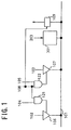
- FIG. 1 there is shown a bus driver failure detection system according to a first preferred embodiment of the present invention.
- the bus driver failure detection system shown is an improvement to the conventional bus driver failure detection system described hereinabove with reference to FIGS. 7 to 9 and includes first and second AND circuits 121 and 122, first and second bus drivers 106 and 107 which output different values to a bus 101, and a receiver 109 for latching a value of the bus 101, similarly to the conventional bus driver failure detection system of FIG. 7.
- the bus driver failure detection system of the present embodiment is different from the conventional bus driver failure detection system in that it additionally includes a bus holding circuit 301 for holding a value of the bus 101.
- the first bus driver 106 outputs, when a first bus driver enable signal 104 is selected, a value of a first output signal 102 to the bus 101 in synchronism with a timing signal 108.
- the second bus driver 107 outputs, when a second bus driver enable signal 105 is selected, a value of a second output signal 103 to the bus 101 in synchronism with the timing signal 108.
- the receiver 109 latches a value of the bus 101 in synchronism with the timing signal 108.
- the bus holding circuit 301 holds a value of the bus 101 only when a test signal 203 is active.
- FIG. 2 particularly shows a circuit construction of the bus driver failure detection system shown in block diagram in FIG. 1 and shows an example of circuit constructions of the first and second bus drivers 106 and 107 and a circuit construction of the bus holding circuit 301.
- the circuit constructions of the first and second bus drivers 106 and 107 are similar to those of the conventional bus driver failure detection system described hereinabove with reference to FIG. 8, and overlapping description of them is omitted here to avoid redundancy. Further, in FIG.
- a waveform 108 indicates a driver enable signal
- another waveform 117 indicates an output of a NAND circuit 117 of the second bus driver 107
- a further waveform 111 indicates an output of a NOR circuit 111 of the first bus driver 106
- a still further waveform 101 indicates a signal potential of the bus 101
- a yet further waveform 109 indicates an output waveform of the receiver 109.
- the bus holding circuit 301 includes a flip-flop formed from a pair of invertors 302 and 303 the input of each of which is connected to the output of the other invertor, and a transfer gate (switch) 304 formed from, for example, an n-channel MOS transistor connected between the output terminal of the invertor 303 (the input terminal of the invertor 302) and the bus 101.
- the test signal 203 is inputted to the control terminal (gate electrode) of the transfer gate 304.
- the dimensions (channel width W and so forth) of the MOS transistor which forms the invertor 303 of the bus holding circuit 301 is smaller than those of the n-channel MOS transistor 113, p-channel MOS transistor 114 and n-channel MOS transistor 118, p-channel MOS transistor 119 which form the first and second bus drivers 106 and 107, respectively, (in other words, the transistor of the invertor 303 has a lower current driving capacity than the output transistors of the drivers) so that, if the output of the invertor 303 and the level of the bus 101 collide with each other, then the level of the n-channel MOS transistor 113 and the p-channel MOS transistor 114 or the n-channel MOS transistor 118 and the p-channel MOS transistor 119 is outputted to the bus 101.
- test signal 203 Upon failure detection, the test signal 203 is rendered active to put the switch 304 into an on state to hold a value of the bus 101 then.
- the bus 101 when the n-channel MOS transistor 113 is normal, the bus 101 exhibits "0" within a period a in FIG. 3 (refer to a solid line portion of the waveform 101 of FIG. 3).
- the gate input of the n-channel MOS transistor 113 exhibits a "0" stuck failure
- the n-channel MOS transistor 113 whose gate potential is kept at a High level remains in an off state within the period a of FIG. 3, and the bus 101 remains holding the value "1" of the preceding cycle (refer to a broken line portion of the waveform 101 of FIG. 3). A failure is detected thereby.
- the bus 101 since the bus 101 holds a value of a preceding cycle with certainty, a failure can be detected without relying upon the rate (cycle) or the layout of the timing signal 108.
- bus holding circuit 301 is connected to the bus 101 only upon testing, the problem of an increase in electric current arising from collision of the level of the bus 101 does not arise in an ordinary operation of the system other than during testing.
- FIG. 4 there is shown in block diagram a construction of a bus driver failure detection system according to another preferred embodiment of the present invention.
- the bus driver failure detection system shown is an improvement to the conventional bus driver failure detection system described hereinabove with reference to FIGS. 7 to 9 and includes first and second AND circuits 121 and 122, first and second bus drivers 106 and 107 which output different values to a bus 101, and a receiver 109 for latching a value of the bus 101, similarly to the conventional bus driver failure detection system of FIG. 7.
- the bus driver failure detection system of the present embodiment is different from the conventional bus driver failure detection system in that it additionally includes a pull-up/pull-down circuit 201 for pulling up/down the bus 101.
- the first bus driver 106 outputs, when a first bus driver enable signal 104 is selected, a value of a first output signal 102 to the bus 101 in synchronism with a timing signal 108.
- the second bus driver 107 outputs, when a second bus driver enable signal 105 is selected, a value of a second output signal 103 to the bus 101 in response to the timing signal 108.
- the receiver 109 latches a value of the bus 101 in synchronism with the timing signal 108.
- the pull-up/pull-down circuit 201 connects a pull-up resistor or a pull-down resistor while a test signal 203 is active.
- FIG. 5 shows an example of a circuit construction of the bus driver failure detection system shown in block diagram in FIG. 4.
- the first and second bus drivers 106 and 107 have similar circuit constructions to those of the conventional bus driver failure detection system described hereinabove with reference to FIG. 8, and overlapping description of them is omitted herein to avoid redundancy.
- the pull-up/pull-down circuit 201 includes a test mode register 202, a NAND circuit 208 to which the test signal 203 and an output of the test mode register 202 are inputted, a NOR circuit 209 to which an inverted signal of the test signal 203 and the output of the test mode register 202 are inputted, a p-channel MOS transistor 206 acting as a switch with the source thereof connected to a power supply, with the gate thereof connected to the output of the NAND circuit 208 and with the drain thereof connected to the bus 101 via a pull-up resistor 204, and an n-channel MOS transistor 207 acting as another switch with the source thereof grounded, with the gate thereof connected to the output of the NOR circuit 209 and with the drain thereof connected to the bus 101 via a pull-down resistor 205.
- test signal 203 Upon failure detection, the test signal 203 is rendered active (changed over to a High level) so that one of the switches 206 and 207 is turned on depending upon the value of the test mode register 202.
- the pull-up resistor 204 or the pull-down resistor 205 is connected to the bus 101.
- the bus 101 exhibits "0" within a period a of FIG. 6 (refer to a solid line portion of the waveform 101 of FIG. 6, but if the gate input of the n-channel MOS transistor 113 exhibits a "0" stuck failure, then the bus 101 now exhibits "1" due to the presence of the pull-up resistor 204 (refer to a broken line portion of the waveform bus 101 of FIG. 6). A failure is detected thereby.
- the pull-up resistor 204 or the pull-down resistor 205 sets the bus 101 to the logic level of "1/0" with certainty, a failure can be detected without relying upon the rate or the layout of the timing signal 108. Further, since the pull-up/pull-down circuit 201 is connected only upon testing, an increase of an electric current which arises from collision of the bus 101 does not occur other than upon testing.
Landscapes
- Engineering & Computer Science (AREA)
- Theoretical Computer Science (AREA)
- General Engineering & Computer Science (AREA)
- Signal Processing (AREA)
- Physics & Mathematics (AREA)
- Computer Networks & Wireless Communication (AREA)
- General Physics & Mathematics (AREA)
- Power Engineering (AREA)
- Human Computer Interaction (AREA)
- Computer Hardware Design (AREA)
- Quality & Reliability (AREA)
- Test And Diagnosis Of Digital Computers (AREA)
- Small-Scale Networks (AREA)
- Debugging And Monitoring (AREA)
Applications Claiming Priority (3)
| Application Number | Priority Date | Filing Date | Title |
|---|---|---|---|
| JP345875/95 | 1995-12-08 | ||
| JP34587595 | 1995-12-08 | ||
| JP7345875A JPH09160690A (ja) | 1995-12-08 | 1995-12-08 | バスドライバ故障検出方式 |
Publications (2)
| Publication Number | Publication Date |
|---|---|
| EP0777328A2 true EP0777328A2 (de) | 1997-06-04 |
| EP0777328A3 EP0777328A3 (de) | 2000-09-20 |
Family
ID=18379589
Family Applications (1)
| Application Number | Title | Priority Date | Filing Date |
|---|---|---|---|
| EP96119025A Withdrawn EP0777328A3 (de) | 1995-12-08 | 1996-11-27 | Fehlererkennungssystem für eine Treiberstufe |
Country Status (5)
| Country | Link |
|---|---|
| US (1) | US5834949A (de) |
| EP (1) | EP0777328A3 (de) |
| JP (1) | JPH09160690A (de) |
| KR (1) | KR970049539A (de) |
| TW (1) | TW330991B (de) |
Families Citing this family (8)
| Publication number | Priority date | Publication date | Assignee | Title |
|---|---|---|---|---|
| US5936424A (en) * | 1996-02-02 | 1999-08-10 | Xilinx, Inc. | High speed bus with tree structure for selecting bus driver |
| US6577157B1 (en) * | 1997-11-14 | 2003-06-10 | Altera Corporation | Fully programmable I/O pin with memory |
| DE10120282B4 (de) * | 2001-04-25 | 2005-08-18 | Infineon Technologies Ag | Bussignalhaltezelle und Verfahren |
| DE102012210106A1 (de) * | 2012-06-15 | 2013-12-19 | Robert Bosch Gmbh | Sensoranordnung für eine Elektrik/Elektronik-Architektur und zugehörige Elektrik/Elektronik-Architektur für ein Fahrzeug |
| US9619310B2 (en) * | 2012-09-26 | 2017-04-11 | Honeywell International Inc. | High speed data transmission methods and systems upon error detection |
| US10425361B2 (en) | 2017-03-16 | 2019-09-24 | Trane International Inc. | Dynamic allocation of termination resistors in a communication network |
| US10664372B2 (en) * | 2018-03-12 | 2020-05-26 | Hamilton Sundstrand Corporation | Data bus and testing system utilizing bus-hold feature |
| CN114646824B (zh) * | 2022-03-11 | 2025-09-09 | 中国船舶重工集团公司第七0七研究所九江分部 | 一种器件输出高阻态的测量电路及方法 |
Family Cites Families (9)
| Publication number | Priority date | Publication date | Assignee | Title |
|---|---|---|---|---|
| US4459693A (en) * | 1982-01-26 | 1984-07-10 | Genrad, Inc. | Method of and apparatus for the automatic diagnosis of the failure of electrical devices connected to common bus nodes and the like |
| JPS6342216A (ja) * | 1986-08-08 | 1988-02-23 | Hitachi Ltd | バイポ−ラトランジスタと電界効果トランジスタとを含む複合回路 |
| US4748426A (en) * | 1986-11-07 | 1988-05-31 | Rodime Plc | Active termination circuit for computer interface use |
| US4841232A (en) * | 1988-04-29 | 1989-06-20 | International Business Machines Corporation | Method and apparatus for testing three state drivers |
| US5039874A (en) * | 1990-03-15 | 1991-08-13 | Hewlett-Packard Company | Method and apparatus for driving an integrated-circuit output pad |
| US5498976A (en) * | 1990-10-26 | 1996-03-12 | Acer Incorporated | Parallel buffer/driver configuration between data sending terminal and data receiving terminal |
| JP3226293B2 (ja) * | 1991-04-24 | 2001-11-05 | 株式会社日立製作所 | 半導体集積回路 |
| US5416784A (en) * | 1991-10-28 | 1995-05-16 | Sequoia Semiconductor | Built-in self-test flip-flop with asynchronous input |
| JPH05304461A (ja) * | 1992-04-07 | 1993-11-16 | Nec Corp | 半導体集積回路 |
-
1995
- 1995-12-08 JP JP7345875A patent/JPH09160690A/ja active Pending
-
1996
- 1996-11-27 US US08/757,998 patent/US5834949A/en not_active Expired - Fee Related
- 1996-11-27 EP EP96119025A patent/EP0777328A3/de not_active Withdrawn
- 1996-12-07 KR KR1019960062796A patent/KR970049539A/ko not_active Ceased
- 1996-12-07 TW TW085115154A patent/TW330991B/zh active
Non-Patent Citations (1)
| Title |
|---|
| None |
Also Published As
| Publication number | Publication date |
|---|---|
| US5834949A (en) | 1998-11-10 |
| TW330991B (en) | 1998-05-01 |
| JPH09160690A (ja) | 1997-06-20 |
| KR970049539A (ko) | 1997-07-29 |
| EP0777328A3 (de) | 2000-09-20 |
Similar Documents
| Publication | Publication Date | Title |
|---|---|---|
| US5293082A (en) | Output driver for reducing transient noise in integrated circuits | |
| US4965474A (en) | Glitch suppression circuit | |
| EP0332077B1 (de) | Bipolar- und CMOS-Transistoren verwendende integrierte Halbleiterschaltung | |
| EP0964519B1 (de) | Integrierte logische Halbleiterschaltung mit sequentiellen Schaltungen zur Unterdrückung von Subschwellenwert-Leckstrom | |
| EP0632594B1 (de) | Verriegelungsgesteuerter Ausgangstreiber | |
| EP0191074B1 (de) | Hilfskreis zur verbesserung der anstiegszeit eines elektronischen signals | |
| JPH08111636A (ja) | プッシュプル出力ドライバ回路 | |
| EP0162932B1 (de) | Datenverarbeitungssystem mit Ausgangsschaltkreis | |
| EP0647028A2 (de) | Verriegelungsschaltungsgesteuerter Ausgangstreiber | |
| US4912339A (en) | Pass gate multiplexer | |
| EP0887935A1 (de) | Störisolierungsschaltung | |
| US5793226A (en) | Data output buffer for multiple power supplies | |
| EP0408032A2 (de) | Steuerschaltung für den Datenausgang für eine Halbleiterspeicheranordnung | |
| US5834949A (en) | Bus driver failure detection system | |
| US5668482A (en) | Bus maintenance circuit | |
| US5739701A (en) | Input/output buffer circuit having reduced power consumption | |
| US5854765A (en) | Semiconductor memory device | |
| US5210449A (en) | Edge triggered tri-state output buffer | |
| US5680065A (en) | Small computer system interface bus driving circuit with unique enable circuitry | |
| US5818264A (en) | Dynamic circuit having improved noise immunity and method therefor | |
| EP0431624B1 (de) | Ausgangsschaltung mit grossem Stromsteuerungsvermögen ohne Erzeugung unerwünschter Spannungsschwankungen | |
| JPH0685648A (ja) | 出力回路 | |
| JPH0771091B2 (ja) | バスドライブ回路 | |
| US5901098A (en) | Ground noise isolation circuit for semiconductor memory device and method thereof | |
| EP0361233B1 (de) | Schaltung zur Unterdrückung von Störsignalen |
Legal Events
| Date | Code | Title | Description |
|---|---|---|---|
| PUAI | Public reference made under article 153(3) epc to a published international application that has entered the european phase |
Free format text: ORIGINAL CODE: 0009012 |
|
| AK | Designated contracting states |
Kind code of ref document: A2 Designated state(s): DE FR GB |
|
| PUAL | Search report despatched |
Free format text: ORIGINAL CODE: 0009013 |
|
| AK | Designated contracting states |
Kind code of ref document: A3 Designated state(s): DE FR GB |
|
| RIC1 | Information provided on ipc code assigned before grant |
Free format text: 7H 03K 19/003 A, 7G 06F 11/267 B |
|
| 17P | Request for examination filed |
Effective date: 20000810 |
|
| 17Q | First examination report despatched |
Effective date: 20010122 |
|
| STAA | Information on the status of an ep patent application or granted ep patent |
Free format text: STATUS: THE APPLICATION IS DEEMED TO BE WITHDRAWN |
|
| 18D | Application deemed to be withdrawn |
Effective date: 20020315 |