EP0777367A1 - Schaltung zur Unterdrückung der Signaldispersion bei Datenübertragung - Google Patents
Schaltung zur Unterdrückung der Signaldispersion bei Datenübertragung Download PDFInfo
- Publication number
- EP0777367A1 EP0777367A1 EP96410118A EP96410118A EP0777367A1 EP 0777367 A1 EP0777367 A1 EP 0777367A1 EP 96410118 A EP96410118 A EP 96410118A EP 96410118 A EP96410118 A EP 96410118A EP 0777367 A1 EP0777367 A1 EP 0777367A1
- Authority
- EP
- European Patent Office
- Prior art keywords
- packet
- bits
- parallel
- transmission
- suppression circuit
- Prior art date
- Legal status (The legal status is an assumption and is not a legal conclusion. Google has not performed a legal analysis and makes no representation as to the accuracy of the status listed.)
- Withdrawn
Links
- 239000006185 dispersion Substances 0.000 title claims abstract description 23
- 230000005540 biological transmission Effects 0.000 claims abstract description 23
- 230000001629 suppression Effects 0.000 claims abstract description 22
- 238000006243 chemical reaction Methods 0.000 claims description 7
- 238000001514 detection method Methods 0.000 claims description 7
- 230000003111 delayed effect Effects 0.000 claims description 2
- 238000005516 engineering process Methods 0.000 description 6
- 230000001934 delay Effects 0.000 description 3
- 238000000034 method Methods 0.000 description 1
- 238000001228 spectrum Methods 0.000 description 1
- 230000001360 synchronised effect Effects 0.000 description 1
Images

Classifications
-
- H—ELECTRICITY
- H04—ELECTRIC COMMUNICATION TECHNIQUE
- H04L—TRANSMISSION OF DIGITAL INFORMATION, e.g. TELEGRAPHIC COMMUNICATION
- H04L25/00—Baseband systems
- H04L25/02—Details ; arrangements for supplying electrical power along data transmission lines
- H04L25/03—Shaping networks in transmitter or receiver, e.g. adaptive shaping networks
- H04L25/03828—Arrangements for spectral shaping; Arrangements for providing signals with specified spectral properties
- H04L25/03866—Arrangements for spectral shaping; Arrangements for providing signals with specified spectral properties using scrambling
Definitions
- the present invention relates to a data processing chain, intended to reduce the number of errors in a transmission.
- the invention relates more particularly to one of the elements of the chain, which is a dispersion suppression circuit also called "descrambling" circuit.
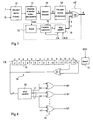
- FIG. 1 represents an example of a processing chain used at the level of a receiver conforming to the European standard for the transmission of digital television signals by satellite.
- digital data is transmitted in byte packets, generally 204 byte packets of which 16 bytes are redundant and are used for error correction. Packet limits are determined by synchronization codes.
- Each packet undergoes a dispersion or "interference" on transmission which serves to reduce the frequency spectrum of the transmission signal in order to facilitate its processing.
- the dispersion consists in combining the bits of each packet by OR-exclusive with corresponding bits supplied by a polynomial counter initialized to an adequate value.
- Each packet also undergoes external coding (Reed-Solomon coding) which generates the aforementioned redundant bytes in order to be able to correct several errors in each packet.
- external coding Random-Solomon coding
- each packet is interleaved in order to better correct bursts of consecutive errors. Indeed, if several consecutive errors occur in the transmission, when the data will have been deinterleaved, the errors of this burst will be in isolated locations and are therefore easier to correct.
- bits to be transmitted undergo internal coding (convolutional coding) to create two redundant transmission signals I and Q which will also be used to reduce the number of errors.
- FIG. 1 represents a part of the architecture according to the aforementioned European standard of the chain of reverse processing of the I and Q signals, on reception.
- the received I and Q signals undergo internal decoding (using the Viterbi algorithm).
- the decoder 10 In the serial signal produced by the decoder 10, synchronization words used to delimit the packets are detected and a series-parallel conversion is carried out to supply bytes.
- deinterlacing In consecutive blocks 14, 16 and 18, deinterlacing, external decoding and dispersion suppression are carried out respectively.
- FIG. 1 the architecture of Figure 1 operates at two different frequencies.
- a first part that is to say the internal decoding circuit 10 and a part of the series-parallel synchronization and conversion circuit 12, are clocked by a fast clock CK at the bit transmission frequency, while the rest of the architecture is clocked by a slower clock CK / 8 at the transmission frequency of the bytes.
- the transmission frequency of the bits is at the limit of what can be obtained with current technologies.
- circuits that operate at this frequency must be made with special care to minimize the clock front delays and to compensate for these delays to work around timing issues. These problems are not encountered in other circuits operating at lower frequencies (CK / 8).
- FIG. 2 represents a conventional dispersion suppression circuit.
- This circuit comprises a polynomial counter consisting of a shift register 20 whose input receives an OR-exclusive combination 22 of the output of the shift register and one or more intermediate flip-flops of this shift register.
- the shift register 20 is clocked by the bit clock CK and receives an initial value at the start of each group of eight packets to be processed. The start of the packet group is determined by a SYNC group synchronization signal.
- the shift register 20 comprises fifteen flip-flops and the input of the register receives the combination by OR-exclusive of the outputs of the last and penultimate flip-flops.
- the initialization value is 100101010000000.
- the output of the OR-exclusive gate 22, constituting the output of the polynomial counter, provides correction bits c to a first input of an OR-exclusive gate 24, at the rate of transmission of the bits.
- B bits of "scrambled" packets are supplied to a second input of gate 24.
- the output of this gate 24 provides bits b 'of "unscrambled" packets.
- the circuit of FIG. 2, particularly simple, is intended to operate on a serial transmission of bits b.
- the dispersion suppression circuit 18 of the architecture of FIG. 1 must work on a parallel transmission of bytes. For this, two solutions could be envisaged.
- a first solution consists in using a parallel arithmetic operating on bytes.
- the resulting circuit, of parallel structure would be complex and would occupy a significant surface compared to the series circuit of figure 2.
- a second solution consists in performing a parallel-series conversion at the output of the external decoder 16 in order to be able to use at 18 the serial circuit of FIG. 2, then to reconvert in parallel the bits supplied in series by the circuit of FIG. 2. If the transmission speed of the bits was slow, this solution would be much less complex than the first solution mentioned above. However, it is always difficult, in any circuit, to pass from a low operating frequency (at the parallel output of the external decoder 16) to a high operating frequency (at the serial input of the circuit of FIG. 2) . The high frequency of the circuit of FIG. 2 must be synchronized with the lower frequency of the decoder 16. This synchronization does not pose any particular problem if the high frequency is far from the technological limits. However, if this high frequency is at the limit of what technology accepts, synchronization becomes particularly delicate and requires the use of complex solutions. In addition, synchronization solutions that will work well in one technology will not necessarily work in another technology.
- An object of the present invention is to provide a dispersion suppression circuit operating in parallel which is of particularly simple structure and which can operate at the limit frequency of the technology employed.
- the present invention provides for performing a series-parallel conversion of the correction bits supplied by a serial polynomial counter.
- the correction bits are therefore supplied by bytes by the serial-parallel converter and can be combined with the bytes of the packet by eight OR-exclusive gates.
- the present invention more particularly provides a dispersion suppression circuit in a transmission of a data packet, comprising a polynomial counter supplying, at the transmission rate of the bits of the packet, correction bits to be combined respectively with the bits of the packet by OU-exclusive.
- the correction bits are supplied to a serial-parallel converter whose output is combined with successive words transmitted in parallel from the packet.
- the polynomial counter is initialized at the start of a packet.
- the dispersion suppression circuit is used in a packet processing chain downstream of a packet synchronization word detection and of a serial-parallel conversion of the transmission of the bits of the packet, the polynomial counter receiving a delayed initialization signal, with respect to a synchronization detection, of the offset between a synchronization detection and the appearance of the start of a packet at the input of the suppression circuit.
- FIG. 3 represents a data processing chain which comprises the same elements as that of FIG. 1, designated by the same references.
- the bytes leaving the external decoder 16 are supplied to a dispersion suppression circuit 18 'according to the present invention.
- This dispersion suppression circuit 18 ′ comprises a series polynomial counter 26, of the type of that of FIG. 2, supplying correction bits c at the bit transmission frequency (CK).
- CK bit transmission frequency
- These correction bits c are supplied to a serial-parallel converter 28 which reconstructs, from bits c, correction bytes C at the rate (CK / 8) of the bytes supplied by the decoder 16.
- These correction bytes C are combined by OR-exclusive in 30 to the bytes leaving the decoder 16.
- the "unscrambled" bytes are formed by the results of these combinations in 30.
- the polynomial counter 26 must be initialized in synchronism with the arrival at the output of the external decoder 16 of the packet starts.
- the packet starts are detected by the synchronization detector 12 which activates a SYNC signal on each detection of a synchronization word defining a packet start.
- This SYNC signal is used to initialize the polynomial counter 26, and is supplied to it via a circuit 32 which delays the SYNC signal so as to initialize the polynomial counter 26 in correspondence with the appearance of the start of a group. of eight packets at the output of the external decoder 16.
- the serial-parallel converter 28 must provide the corresponding correction byte C.
- the polynomial counter 26 must have been initialized eight cycles of the clock bit CK earlier.
- a parallel dispersion suppression circuit according to the present invention occupies an area comparable to that occupied by the series circuit of FIG. 2.
- a parallel-series converter is not used which, as explained above, has huge problems with switching from a slow frequency (byte frequency) to a fast frequency (bit frequency) at the limit of what the technology used accepts.
- a time base which comprises a packet counter initialized by the synchronization circuit 12 at each start of a group of eight packets, and a counter d bytes initialized by the synchronization circuit 12 at each start of a packet.
- the packet counter indicates the rank of a current packet in the current group
- the byte counter indicates the rank of a current byte in the current packet (a current byte being that provided by the serial converter - parallel 12).
- Delay 32 is then obtained while waiting for the packet and byte counters to reach corresponding values.
- the packets to be processed comprise 204 bytes and the delay introduced by blocks 14 and 16 is 1157 bytes.
- the polynomial counter 28 is initialized when the packet and byte counters reach the value 5 and the value 136, respectively.
- FIG. 4 represents a detailed embodiment of the dispersion suppression circuit 18 '.
- the polynomial counter 26, comprising a shift register 20 and an OR-exclusive gate 22, is identical to that of FIG. 2.
- the shift register 20 is clocked by the bit clock CK and it is initialized via the delay circuit 32.
- the output of the OR-exclusive gate 22, delivering in series correction bits c, is supplied to the serial-parallel converter 28.
- Each of eight OR-exclusive gates 30 receives a bit corresponding to "scrambled" bytes "and a corresponding bit of the correction byte C supplied by the parallel serial converter 28.
- the outputs of the OR-exclusive gates 30 supply the bits b 'of each of the" unscrambled "bytes.
Landscapes
- Engineering & Computer Science (AREA)
- Physics & Mathematics (AREA)
- Spectroscopy & Molecular Physics (AREA)
- Power Engineering (AREA)
- Computer Networks & Wireless Communication (AREA)
- Signal Processing (AREA)
- Synchronisation In Digital Transmission Systems (AREA)
- Error Detection And Correction (AREA)
- Detection And Prevention Of Errors In Transmission (AREA)
Applications Claiming Priority (2)
| Application Number | Priority Date | Filing Date | Title |
|---|---|---|---|
| FR9514383 | 1995-11-30 | ||
| FR9514383A FR2742016B1 (fr) | 1995-11-30 | 1995-11-30 | Circuit de suppression de dispersion dans une transmission de donnees |
Publications (1)
| Publication Number | Publication Date |
|---|---|
| EP0777367A1 true EP0777367A1 (de) | 1997-06-04 |
Family
ID=9485173
Family Applications (1)
| Application Number | Title | Priority Date | Filing Date |
|---|---|---|---|
| EP96410118A Withdrawn EP0777367A1 (de) | 1995-11-30 | 1996-11-22 | Schaltung zur Unterdrückung der Signaldispersion bei Datenübertragung |
Country Status (3)
| Country | Link |
|---|---|
| US (1) | US5784013A (de) |
| EP (1) | EP0777367A1 (de) |
| FR (1) | FR2742016B1 (de) |
Families Citing this family (3)
| Publication number | Priority date | Publication date | Assignee | Title |
|---|---|---|---|---|
| KR100219481B1 (ko) * | 1996-05-23 | 1999-09-01 | 윤종용 | 시디롬 디코더의 디스크램블링 데이타 생성방법 및그장치와이를이용한디스크램블러 |
| US6636607B1 (en) * | 1998-10-08 | 2003-10-21 | Ati International Srl | Method and apparatus for controlling display of content signals |
| US6976265B1 (en) | 1998-10-08 | 2005-12-13 | Ati International Srl | Method and apparatus for controlling display of content signals |
Citations (4)
| Publication number | Priority date | Publication date | Assignee | Title |
|---|---|---|---|---|
| EP0488325A2 (de) * | 1990-11-28 | 1992-06-03 | Siemens Aktiengesellschaft | Bei Sonet-Datenübertragung gebutzter, paralleler Verschlüssler |
| EP0549047A1 (de) * | 1991-12-20 | 1993-06-30 | Koninklijke KPN N.V. | Scrambler, Descrambler und Synchronisierer für ein Datenübertragungssystem |
| US5241602A (en) * | 1992-02-07 | 1993-08-31 | Byeong Gi Lee | Parallel scrambling system |
| EP0566330A2 (de) * | 1992-04-16 | 1993-10-20 | AT&T Corp. | Mehrpegelkodierung mit Trellis-kodierter Modulation und Reed-Solomon-Koden |
Family Cites Families (1)
| Publication number | Priority date | Publication date | Assignee | Title |
|---|---|---|---|---|
| US5185799A (en) * | 1990-11-28 | 1993-02-09 | Siemens Aktiengesellschaft | Parallel scrambler used in SONET data transmission |
-
1995
- 1995-11-30 FR FR9514383A patent/FR2742016B1/fr not_active Expired - Fee Related
-
1996
- 1996-11-22 EP EP96410118A patent/EP0777367A1/de not_active Withdrawn
- 1996-11-25 US US08/755,197 patent/US5784013A/en not_active Expired - Lifetime
Patent Citations (4)
| Publication number | Priority date | Publication date | Assignee | Title |
|---|---|---|---|---|
| EP0488325A2 (de) * | 1990-11-28 | 1992-06-03 | Siemens Aktiengesellschaft | Bei Sonet-Datenübertragung gebutzter, paralleler Verschlüssler |
| EP0549047A1 (de) * | 1991-12-20 | 1993-06-30 | Koninklijke KPN N.V. | Scrambler, Descrambler und Synchronisierer für ein Datenübertragungssystem |
| US5241602A (en) * | 1992-02-07 | 1993-08-31 | Byeong Gi Lee | Parallel scrambling system |
| EP0566330A2 (de) * | 1992-04-16 | 1993-10-20 | AT&T Corp. | Mehrpegelkodierung mit Trellis-kodierter Modulation und Reed-Solomon-Koden |
Also Published As
| Publication number | Publication date |
|---|---|
| FR2742016A1 (fr) | 1997-06-06 |
| FR2742016B1 (fr) | 1998-02-13 |
| US5784013A (en) | 1998-07-21 |
Similar Documents
| Publication | Publication Date | Title |
|---|---|---|
| EP0552979B1 (de) | Gerät und Verfahren zum Entschachteln von Daten | |
| FR2515459A1 (fr) | Systeme d'affichage de television a artefacts de balayage de ligne reduits | |
| FR2466837A1 (fr) | Memoire tampon d'interface terrestre a acces multiples par repartition de temps pour operations entrelacees | |
| FR2687262A1 (fr) | Systeme d'embrouillage parallele. | |
| FR2600478A1 (fr) | Procede et dispositif pour geler une image de television | |
| FR2693860A1 (fr) | Convertisseur parallèle-série. | |
| EP0161177B1 (de) | Verfahren und Einrichtung zur Wiedergewinnung des Rahmenverriegelungswortes mit verteilten Bits in einem digitalen Signal | |
| FR2582893A1 (fr) | Circuit d'elaboration des signaux analogiques de couleurs primaires d'un signal de television a partir de ses composantes numeriques de luminance et de chrominance. | |
| EP0840958B1 (de) | Ver- und entschachtelung von datenelementen | |
| EP0680170B1 (de) | Übertragungsanordnung für ein Leitungskodiertes Signal über eine Fernsprechleitung mit Frequenzsynchronisierungsschaltung | |
| EP0027423A1 (de) | Einrichtung zur Verschlüsselung und Entschlüsselung eines digitalen Signals | |
| EP0581375A1 (de) | Verfahren zum Verändern von Pseudozufallsfolgen und Vorrichtung zum Ver- oder Entschlüsseln von Informationen | |
| EP0041001A1 (de) | Digitale Bit-für-Bit Zeitmultiplex-Fernmeldekoppelfelder | |
| EP0777367A1 (de) | Schaltung zur Unterdrückung der Signaldispersion bei Datenübertragung | |
| FR2549331A1 (fr) | Dispositif pour ajuster differentiellement la phase des signaux analogiques dans un systeme de traitement de signaux video | |
| EP0082529B1 (de) | Digitaler Echounterdrücker | |
| FR2664769A1 (fr) | Dispositif d'echantillonnage de donnees et systeme de transmission numerique de donnees en resultant. | |
| EP0126495B1 (de) | Entzerrer für durch zyklische Verwechslung verschlüsselte Fernsehbilder | |
| FR2500245A1 (fr) | Systeme de traitement de signaux echantillonnes de television, systeme de transmission de signaux numeriques de television en couleur, procede de transcodage et recepteur de signaux numeriques de television | |
| EP0528738B1 (de) | Verfahren und Schaltung zur Koeffizientenanpassung im Entzerrer eines Modems | |
| FR2710208A1 (fr) | Intégrateur et filtre du premier ordre numériques. | |
| EP0424269A1 (de) | Gerät zur Bewegungskompensation und Fernsehempfänger mit einem solchen Gerät | |
| EP0194186B1 (de) | Verfahren zur Übertragung von Daten durch Einfügen in ein analoges Sprachsignal und Vorrichtungen zur Durchführung dieses Verfahrens | |
| EP0620641A1 (de) | Signalverarbeitungsanordnung mit mehreren verschiedenen Filtern, insbesondere für audiofrequente Codierung von Stimmensignalen | |
| FR2584256A1 (fr) | Procede de multiplexage et de demultiplexage temporels de signaux video et de signaux a bande etroite, et dispositifs pour la mise en oeuvre de ce procede |
Legal Events
| Date | Code | Title | Description |
|---|---|---|---|
| PUAI | Public reference made under article 153(3) epc to a published international application that has entered the european phase |
Free format text: ORIGINAL CODE: 0009012 |
|
| AK | Designated contracting states |
Kind code of ref document: A1 Designated state(s): DE FR GB IT |
|
| 17P | Request for examination filed |
Effective date: 19971110 |
|
| RAP3 | Party data changed (applicant data changed or rights of an application transferred) |
Owner name: STMICROELECTRONICS S.A. |
|
| RAP1 | Party data changed (applicant data changed or rights of an application transferred) |
Owner name: STMICROELECTRONICS S.A. |
|
| 17Q | First examination report despatched |
Effective date: 20030905 |
|
| STAA | Information on the status of an ep patent application or granted ep patent |
Free format text: STATUS: THE APPLICATION IS DEEMED TO BE WITHDRAWN |
|
| 18D | Application deemed to be withdrawn |
Effective date: 20041230 |