EP0778657A1 - Flaches elektromagnetisches betätigungsorgan - Google Patents
Flaches elektromagnetisches betätigungsorgan Download PDFInfo
- Publication number
- EP0778657A1 EP0778657A1 EP96912255A EP96912255A EP0778657A1 EP 0778657 A1 EP0778657 A1 EP 0778657A1 EP 96912255 A EP96912255 A EP 96912255A EP 96912255 A EP96912255 A EP 96912255A EP 0778657 A1 EP0778657 A1 EP 0778657A1
- Authority
- EP
- European Patent Office
- Prior art keywords
- magnetic field
- movable plate
- electromagnetic actuator
- movable portion
- static magnetic
- Prior art date
- Legal status (The legal status is an assumption and is not a legal conclusion. Google has not performed a legal analysis and makes no representation as to the accuracy of the status listed.)
- Granted
Links
- 230000003068 static effect Effects 0.000 claims abstract description 35
- 238000010276 construction Methods 0.000 claims abstract description 25
- 239000000758 substrate Substances 0.000 claims description 16
- 238000009413 insulation Methods 0.000 claims description 10
- 230000002093 peripheral effect Effects 0.000 claims description 6
- 239000004065 semiconductor Substances 0.000 claims description 5
- 229910052761 rare earth metal Inorganic materials 0.000 claims description 3
- 150000002910 rare earth metals Chemical class 0.000 claims description 3
- XUIMIQQOPSSXEZ-UHFFFAOYSA-N Silicon Chemical compound [Si] XUIMIQQOPSSXEZ-UHFFFAOYSA-N 0.000 description 8
- 229910052710 silicon Inorganic materials 0.000 description 8
- 239000010703 silicon Substances 0.000 description 8
- BGPVFRJUHWVFKM-UHFFFAOYSA-N N1=C2C=CC=CC2=[N+]([O-])C1(CC1)CCC21N=C1C=CC=CC1=[N+]2[O-] Chemical compound N1=C2C=CC=CC2=[N+]([O-])C1(CC1)CCC21N=C1C=CC=CC1=[N+]2[O-] BGPVFRJUHWVFKM-UHFFFAOYSA-N 0.000 description 6
- 238000010586 diagram Methods 0.000 description 4
- 238000004519 manufacturing process Methods 0.000 description 4
- 238000000034 method Methods 0.000 description 4
- 230000000694 effects Effects 0.000 description 3
- 230000004907 flux Effects 0.000 description 3
- RYGMFSIKBFXOCR-UHFFFAOYSA-N Copper Chemical compound [Cu] RYGMFSIKBFXOCR-UHFFFAOYSA-N 0.000 description 2
- XEEYBQQBJWHFJM-UHFFFAOYSA-N Iron Chemical compound [Fe] XEEYBQQBJWHFJM-UHFFFAOYSA-N 0.000 description 2
- 238000006243 chemical reaction Methods 0.000 description 2
- 229910052802 copper Inorganic materials 0.000 description 2
- 239000010949 copper Substances 0.000 description 2
- 238000005516 engineering process Methods 0.000 description 2
- XAGFODPZIPBFFR-UHFFFAOYSA-N aluminium Chemical compound [Al] XAGFODPZIPBFFR-UHFFFAOYSA-N 0.000 description 1
- 229910052782 aluminium Inorganic materials 0.000 description 1
- 239000004020 conductor Substances 0.000 description 1
- 125000004122 cyclic group Chemical group 0.000 description 1
- 238000006073 displacement reaction Methods 0.000 description 1
- 238000009429 electrical wiring Methods 0.000 description 1
- 238000005530 etching Methods 0.000 description 1
- 229910052742 iron Inorganic materials 0.000 description 1
- 238000007740 vapor deposition Methods 0.000 description 1
Images

Classifications
-
- G—PHYSICS
- G02—OPTICS
- G02B—OPTICAL ELEMENTS, SYSTEMS OR APPARATUS
- G02B26/00—Optical devices or arrangements for the control of light using movable or deformable optical elements
- G02B26/08—Optical devices or arrangements for the control of light using movable or deformable optical elements for controlling the direction of light
- G02B26/0816—Optical devices or arrangements for the control of light using movable or deformable optical elements for controlling the direction of light by means of one or more reflecting elements
- G02B26/0833—Optical devices or arrangements for the control of light using movable or deformable optical elements for controlling the direction of light by means of one or more reflecting elements the reflecting element being a micromechanical device, e.g. a MEMS mirror, DMD
- G02B26/085—Optical devices or arrangements for the control of light using movable or deformable optical elements for controlling the direction of light by means of one or more reflecting elements the reflecting element being a micromechanical device, e.g. a MEMS mirror, DMD the reflecting means being moved or deformed by electromagnetic means
-
- G—PHYSICS
- G02—OPTICS
- G02B—OPTICAL ELEMENTS, SYSTEMS OR APPARATUS
- G02B26/00—Optical devices or arrangements for the control of light using movable or deformable optical elements
- G02B26/08—Optical devices or arrangements for the control of light using movable or deformable optical elements for controlling the direction of light
- G02B26/10—Scanning systems
- G02B26/101—Scanning systems with both horizontal and vertical deflecting means, e.g. raster or XY scanners
-
- H—ELECTRICITY
- H02—GENERATION; CONVERSION OR DISTRIBUTION OF ELECTRIC POWER
- H02K—DYNAMO-ELECTRIC MACHINES
- H02K33/00—Motors with reciprocating, oscillating or vibrating magnet, armature or coil system
- H02K33/18—Motors with reciprocating, oscillating or vibrating magnet, armature or coil system with coil systems moving upon intermittent or reversed energisation thereof by interaction with a fixed field system, e.g. permanent magnets
Definitions
- the present invention relates to a planar type electromagnetic actuator in which miniaturization has been realized through the use of semiconductor manufacturing technology, and in particular to a technique for reducing the cost of planar type electromagnetic actuators.
- the present inventor has previously proposed a very small size planar type electromagnetic actuator which utilizes semiconductor technology.
- This device is suitable for example for a planar type mirror galvanometer (Japanese Patent Application Nos. 5-320524 and 6-9824).
- the electromagnetic actuator comprises a silicon substrate on which is integrally formed a planar movable portion, and an axial support portion of torsion bar construction for axially supporting the movable portion so as to be able to swing at a central location of the movable portion relative to the silicon substrate in a perpendicular direction thereof.
- permanent magnets serving as static magnetic field generating devices forming a pair with each other, are provided at the periphery of the movable portion so that the static magnetic field generated thereby ads on the planar coil portions located on the opposite sides of the movable portion which are parallel with the axial direction of the axial support portion.
- pairs of permanent magnets are respectively located above and below the opposite side portions of the movable portion, the construction being such that the static magnetic fields generated between the pairs of permanent magnets intersect the drive coil in predetermined directions.
- Such an electromagnetic actuator is driven by passing a current through the planar coil. That is to say, a static magnetic field is formed by means of the permanent magnets on opposite sides of the movable portion in a direction so as to intersect the planar coil lying along the planar face of the movable portion.
- a magnetic force acts in a direction according to Fleming's left hand rule for current, magnetic flux density, and force, on the opposite sides of the movable portion in proportion to the current density and magnetic flux density of the planar coil, as represented by the following equation (1), so that the movable portion is rotated.
- F i x B
- the axial support portion is twisted with the rotation of the movable portion, producing a spring reaction force, so that the movable portion rotates to a position where the magnetic force and the spring reaction force are in equilibrium.
- the angle of rotation of the moveable portion is proportional to the current flowing in the planar coil, and hence the rotation angle of the movable portion can be controlled by controlling the current flowing in the planar coil.
- the device can be used as a mirror galvanometer for carrying out laser beam scanning by cyclic operation to continuously change the mirror displacement angle.
- One such electromagnetic actuator has a two axis construction with two axial support portions at right angles to each other.
- the movable portion formed integral with the silicon substrate is made up of a frame like outer movable plate and a planar inner movable plate located within the frame of the outer movable plate.
- the axial support portions comprise first torsion bars for axially supporting the outer movable plate, and a second torsion bars aligned perpendicular to the first torsion bars, for axially supporting the inner movable plate relative to the outer movable plate.
- respective drive coils are provided on the upper surfaces of the outer and inner movable plates.
- the permanent magnets for driving the outer movable plate and the permanent magnets for driving the inner movable plate are provided separate to each other.
- the mutually opposing permanent magnets act in pairs to generate mutually perpendicular magnetic fields relative to the movable portion. That is to say, with the conventional construction, at least four permanent magnets, in other words two pairs of static magnetic field generating devices, are required.
- the present invention takes into consideration the above situation with the object of providing an electromagnetic actuator wherein the construction is simplified and manufacturing costs reduced, by having only one pair of static magnetic field generating devices for generating static magnetic fields mutually perpendicular to the movable portion.
- the construction incorporates: a movable portion comprising a frame like outer movable plate and an inner movable plate located within the outer movable plate, and an axial support portion comprising first torsion bars for axially supporting the outer movable plate so as to be able to swing, and second torsion bars aligned axially at right angles to the first torsion bars, for axially supporting the inner movable plate so as to be able to swing, integrally formed on a semiconductor substrate; drive coils provided on respective peripheral portions of the outer movable plate and inner movable plate; and static magnetic field generating devices for applying a static magnetic field to the drive coils, the construction being such that the movable portion is driven by a magnetic field produced by passing a current through the drive coils, and is characterized in that one pair of the static magnetic field generating devices are provided on one diagonal line of the movable portion with the movable portion therebetween.
- the construction may be such that the pair of static magnetic field generating devices are fixed to a yoke made from a magnetic body and located surrounding the movable portion.
- the pair of static magnetic field generating means may be permanent magnets located with a north pole and south pole facing each other.
- the permanent magnet may be rare earth type magnets.
- a mirror galvanometer may be formed with a reflective mirror on a central face of the inner movable plate of the movable portion.
- the basic construction of the mirror galvanometer may include; a movable portion incorporating the reflective mirror, a scanner body provided with an axial support portion and a drive coil, a yoke comprising a frame shape magnetic body surrounding the scanner body, and permanent magnets secured to the yoke and aligned with one diagonal direction of the scanner body with the scanner body therebetween, arranged on an insulation substrate, and a plurality of electrical terminal pins electrically connected to the drive coil and fitted to the insulation substrate.
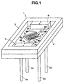
- FIG. 1 shows the construction of an embodiment of an electromagnetic actuator according to the present invention applied to a mirror galvanometer.
- a mirror galvanometer 1 being the electromagnetic actuator of this embodiment, has a scanner body 10 with a movable portion and an axial support portion formed integrally on a semiconductor substrate such as a silicon substrate, positioned centrally on an insulation plate 2 and inclined at 45 degrees to the insulation plate 2 as shown in the figure.
- a frame like yoke 3 made for example from a magnetic body such as pure iron, is provided on an upper peripheral face of the insulation plate 2.
- a pair of permanent magnets 4, 5 serving as static magnetic field generating devices, are provided on the inside of two mutually facing sides of the yoke 3.
- the south and north poles face each other so that a static magnetic field is produced from one permanent magnet 4 (or 5) towards the other permanent magnet 5 (or 4), intersecting the scanner body 10.
- the static magnetic field is produced from the permanent magnet 4 towards the permanent magnet 5.
- connector pins 6a ⁇ 6d serving as electrical terminal pins, are fitted to the insulation plate 2.
- the respective connector pins 6a ⁇ 6d are electrically connected to four bonding pads 7a ⁇ 7d which are formed on the insulation plate 2.
- Respective planar coils 15A, 15B of the scanner body 10 are connected to the respective bonding pads 7a ⁇ 7d via conductors 8a ⁇ 8d.
- the construction is such that for example the connector pins 6a, 6b and 6c, 6d are in respective pairs, with one as a positive pole and the other as a negative pole, and power is conducted via the connector pins 6a, 6b to the planar coil 15A of the outer movable plate 12A (to be described later), and via the connector pins 6c, 6d to the planar coil 15B of the inner movable plate 12B (to be described later).
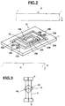
- a movable portion comprising a frame like outer movable plate 12A and a planar inner movable plate 12B, and an axial support portion comprising first torsion bars 13A, 13A for axially supporting the outer movable plate 12A, and second torsion bars 13B, 13B for axially supporting the inner movable plate 12B relative to the outer movable plate 12A formed with their axes at right angles to each other, are integrally formed on a silicon substrate 11 by anisotropic etching.
- the thickness of the movable portion is made thin compared to the thickness of the silicon substrate 11, so that the movable portion can swing about the axial support portion.
- a planar coil 15A (shown typically as a single line in FIG. 2) of for example a thin copper film serving as a drive coil, is formed using an electro-typing method or the like, on the upper face of the outer movable plate 12A, and is electrically connected to a pair of outer electrode terminals 14A, 14A on the silicon substrate 11, by way of one of the first torsion bars 13A, 13A.
- a planar coil 15B (shown typically as a single line in FIG.
- a drive coil serving as a drive coil, is formed by the same method as for the planar coil 15A, on the upper face peripheral portion of the inner movable plate 12B, and is electrically connected to a pair of inner electrode terminals 14B, 14B on the silicon substrate 11, by way of the other of the first torsion bars 13A, 13A, passing from one of the second torsion bars 13B, 13B via the outer movable plate 12A portion.
- a total reflection mirror 16 made for example by aluminum vapor deposition, is formed on the upper face central portion of the inner movable plate 12B.
- the pair of outer electrode terminals 14A, 14A, and inner electrode terminals 14B, 14B are formed similarly to the planar coils 15A, 15B, by an electro-typing method or the like.
- the magnetic field produced by the permanent magnet 4 is directed towards the permanent magnet 5, intersecting the scanner body 10 on the insulation substrate 2.
- the magnetic field H has a transverse component magnetic field H 1 and a longitudinal component magnetic field H 2 intersecting at right angles to each other in the plane of the scanner body 10.
- the transverse component magnetic field H 1 is aligned at right angles to the axial direction of the first torsion bars 13A, 13A for axially supporting the outer movable plate 12A
- the longitudinal component magnetic field H 2 is aligned at right angles to the axial direction of the second torsion bars 13B, 13B for axially supporting the inner movable plate 12B.
- the outer movable plate 12A and the inner movable plate 12B can be driven with only one pair of permanent magnets 4, 5, and hence there is no need to provide separate permanent magnets for respectively driving the outer movable plate and the inner movable plate, as with the conventional arrangement. Therefore, the number of components for the electromagnetic actuator can be reduced and the construction simplified, and hence the manufacturing costs for the electromagnetic actuator can be reduced.
- the efficiency of the magnetic field produced by the permanent magnets 4, 5 can be increased so that a large magnetic force can be obtained.
- FIG. 4 (A) there is an ineffective magnetic field at the peripheries of the permanent magnets 4 and 5 as shown by the dotted line, which does not intersect the scanner body 10 and thus has no relation to movement of the movable portion.
- the ineffective magnetic field can be guided to the other permanent magnet as an effective magnetic field H.
- the amount of ineffective magnetic field can be reduced, and the effective magnetic field shown by the full lines in the figure, which intersects the scanner body 10 and thus contributes to the drive of the movable portion, increased. Consequently, in the case where permanent magnets of the same properties are used, then by providing the yoke 3, the efficiency of the permanent magnets can be increased compared to when the yoke is not provided, so that a large magnetic force can be obtained.
- An electromagnet may also be used for the static magnetic field generating device.
- electrical wiring is required.
- the construction using the permanent magnets as with the present embodiment is simpler and thus more desirable.
- a rare earth type magnet by using a rare earth type magnet, a large magnetic field H can be obtained, and the magnetic force thus increased.
- the example given for the present embodiment has been for an electromagnetic actuator applied to a planar type mirror galvanometer.
- the invention is not limited to this.
- the pair of static magnetic field generating devices are provided aligned with the diagonal direction of the movable portion which has two movable plates axially supported at right angles to each other, then the two movable plates can be driven with only one pair of static magnetic field generating devices.
- the number of components for the electromagnetic actuator can thus be reduced and the construction simplified, and hence the manufacturing costs for the electromagnetic actuator can be greatly reduced.
- a yoke is provided, then the efficiency of the static magnetic field generating devices can be increased, and hence the drive force for the movable portion thus increased.
- the present invention enables a simplification and reduction in cost of instruments which incorporate very small size planar type electromagnetic actuators, and hence industrial applicability is considerable.
Landscapes
- Physics & Mathematics (AREA)
- General Physics & Mathematics (AREA)
- Optics & Photonics (AREA)
- Engineering & Computer Science (AREA)
- Power Engineering (AREA)
- Electromagnetism (AREA)
- Mechanical Optical Scanning Systems (AREA)
- Reciprocating, Oscillating Or Vibrating Motors (AREA)
- Apparatuses For Generation Of Mechanical Vibrations (AREA)
- Micromachines (AREA)
Applications Claiming Priority (4)
| Application Number | Priority Date | Filing Date | Title |
|---|---|---|---|
| JP12805695 | 1995-05-26 | ||
| JP128056/95 | 1995-05-26 | ||
| JP7128056A JP2987750B2 (ja) | 1995-05-26 | 1995-05-26 | プレーナ型電磁アクチュエータ |
| PCT/JP1996/001149 WO1996037943A1 (fr) | 1995-05-26 | 1996-04-26 | Actionneur electromagnetique plat |
Publications (3)
| Publication Number | Publication Date |
|---|---|
| EP0778657A1 true EP0778657A1 (de) | 1997-06-11 |
| EP0778657A4 EP0778657A4 (de) | 1998-02-04 |
| EP0778657B1 EP0778657B1 (de) | 2001-09-19 |
Family
ID=14975400
Family Applications (1)
| Application Number | Title | Priority Date | Filing Date |
|---|---|---|---|
| EP96912255A Expired - Lifetime EP0778657B1 (de) | 1995-05-26 | 1996-04-26 | Flaches elektromagnetisches betätigungsorgan |
Country Status (6)
| Country | Link |
|---|---|
| US (1) | US5912608A (de) |
| EP (1) | EP0778657B1 (de) |
| JP (1) | JP2987750B2 (de) |
| KR (1) | KR100402264B1 (de) |
| DE (1) | DE69615321T2 (de) |
| WO (1) | WO1996037943A1 (de) |
Cited By (10)
| Publication number | Priority date | Publication date | Assignee | Title |
|---|---|---|---|---|
| EP1037009A1 (de) * | 1999-03-09 | 2000-09-20 | Nanosurf AG | Mehrachsiger Aktuator und Messkopf für ein Rastersondenmikroskop |
| WO2001078096A3 (en) * | 2000-04-07 | 2002-04-04 | Microsoft Corp | Magnetically actuated microelectromechanical systems actuator |
| EP1207416A1 (de) * | 2000-11-20 | 2002-05-22 | Olympus Optical Co., Ltd. | Optischer Deflektor |
| WO2002025349A3 (en) * | 2000-09-19 | 2003-09-25 | Draper Lab Charles S | Multi-axis magnetically actuated device |
| DE102008001056A1 (de) | 2008-04-08 | 2009-10-15 | Robert Bosch Gmbh | Umlenkeinrichtung für einen Strahl einer elektromagnetischen Welle |
| WO2009141021A1 (de) * | 2008-05-21 | 2009-11-26 | Robert Bosch Gmbh | Magnetjoch, mikromechanisches bauteil und herstellungsverfahren für ein magnetjoch und ein mikromechanisches bauteil |
| DE102008001893A1 (de) | 2008-05-21 | 2009-11-26 | Robert Bosch Gmbh | Umlenkeinrichtung für elektromagnetische Strahlen |
| CN102540458A (zh) * | 2010-12-08 | 2012-07-04 | 精工爱普生株式会社 | 致动器、光学扫描仪及图像形成装置 |
| CN107907993A (zh) * | 2017-12-08 | 2018-04-13 | 上海禾赛光电科技有限公司 | 谐振式扫描镜、扫描方法、角度的测量方法及加工方法 |
| US10690906B2 (en) | 2010-12-08 | 2020-06-23 | Robert Bosch Gmbh | Magnetic actuator |
Families Citing this family (134)
| Publication number | Priority date | Publication date | Assignee | Title |
|---|---|---|---|---|
| US6201629B1 (en) | 1997-08-27 | 2001-03-13 | Microoptical Corporation | Torsional micro-mechanical mirror system |
| JP4414498B2 (ja) * | 1997-12-09 | 2010-02-10 | オリンパス株式会社 | 光偏向器 |
| US7170665B2 (en) | 2002-07-24 | 2007-01-30 | Olympus Corporation | Optical unit provided with an actuator |
| US6303986B1 (en) | 1998-07-29 | 2001-10-16 | Silicon Light Machines | Method of and apparatus for sealing an hermetic lid to a semiconductor die |
| US6872984B1 (en) | 1998-07-29 | 2005-03-29 | Silicon Light Machines Corporation | Method of sealing a hermetic lid to a semiconductor die at an angle |
| US6014257A (en) * | 1998-10-14 | 2000-01-11 | Eastman Kodak Company | Light modulator |
| US5991079A (en) * | 1998-10-14 | 1999-11-23 | Eastman Kodak Company | Method of making a light modulator |
| US6088148A (en) * | 1998-10-30 | 2000-07-11 | Eastman Kodak Company | Micromagnetic light modulator |
| JP4111619B2 (ja) * | 1999-02-26 | 2008-07-02 | 日本信号株式会社 | プレーナ型光走査装置の実装構造 |
| CA2328201A1 (en) * | 1999-03-18 | 2000-09-21 | Trustees Of Boston University | Very large angle integrated optical scanner made with an array of piezoelectric monomorphs |
| US6201631B1 (en) * | 1999-10-08 | 2001-03-13 | Lucent Technologies Inc. | Process for fabricating an optical mirror array |
| US6753638B2 (en) | 2000-02-03 | 2004-06-22 | Calient Networks, Inc. | Electrostatic actuator for micromechanical systems |
| US6956878B1 (en) | 2000-02-07 | 2005-10-18 | Silicon Light Machines Corporation | Method and apparatus for reducing laser speckle using polarization averaging |
| NL1015131C1 (nl) * | 2000-04-16 | 2001-10-19 | Tmp Total Micro Products B V | Inrichting en werkwijze voor het schakelen van elektromagnetische signalen of bundels. |
| US6628041B2 (en) | 2000-05-16 | 2003-09-30 | Calient Networks, Inc. | Micro-electro-mechanical-system (MEMS) mirror device having large angle out of plane motion using shaped combed finger actuators and method for fabricating the same |
| US6585383B2 (en) | 2000-05-18 | 2003-07-01 | Calient Networks, Inc. | Micromachined apparatus for improved reflection of light |
| US6560384B1 (en) | 2000-06-01 | 2003-05-06 | Calient Networks, Inc. | Optical switch having mirrors arranged to accommodate freedom of movement |
| US6728016B1 (en) | 2000-06-05 | 2004-04-27 | Calient Networks, Inc. | Safe procedure for moving mirrors in an optical cross-connect switch |
| US6587611B1 (en) | 2000-06-06 | 2003-07-01 | Calient Networks, Inc. | Maintaining path integrity in an optical switch |
| US6989921B2 (en) * | 2000-08-27 | 2006-01-24 | Corning Incorporated | Magnetically actuated micro-electro-mechanical apparatus and method of manufacture |
| US6825967B1 (en) | 2000-09-29 | 2004-11-30 | Calient Networks, Inc. | Shaped electrodes for micro-electro-mechanical-system (MEMS) devices to improve actuator performance and methods for fabricating the same |
| JP3926552B2 (ja) * | 2000-10-25 | 2007-06-06 | 日本信号株式会社 | アクチュエ−タ |
| US6775048B1 (en) | 2000-10-31 | 2004-08-10 | Microsoft Corporation | Microelectrical mechanical structure (MEMS) optical modulator and optical display system |
| JP4544734B2 (ja) * | 2000-12-21 | 2010-09-15 | シチズンファインテックミヨタ株式会社 | プレーナー型ガルバノミラー |
| US7177081B2 (en) | 2001-03-08 | 2007-02-13 | Silicon Light Machines Corporation | High contrast grating light valve type device |
| US6792177B2 (en) | 2001-03-12 | 2004-09-14 | Calient Networks, Inc. | Optical switch with internal monitoring |
| US6912078B2 (en) | 2001-03-16 | 2005-06-28 | Corning Incorporated | Electrostatically actuated micro-electro-mechanical devices and method of manufacture |
| US6707591B2 (en) | 2001-04-10 | 2004-03-16 | Silicon Light Machines | Angled illumination for a single order light modulator based projection system |
| JP2002307396A (ja) * | 2001-04-13 | 2002-10-23 | Olympus Optical Co Ltd | アクチュエータ |
| US6813055B2 (en) * | 2001-05-30 | 2004-11-02 | Fiberyard, Inc. | Optical beam steering device |
| US6865346B1 (en) | 2001-06-05 | 2005-03-08 | Silicon Light Machines Corporation | Fiber optic transceiver |
| US6747781B2 (en) | 2001-06-25 | 2004-06-08 | Silicon Light Machines, Inc. | Method, apparatus, and diffuser for reducing laser speckle |
| US6782205B2 (en) | 2001-06-25 | 2004-08-24 | Silicon Light Machines | Method and apparatus for dynamic equalization in wavelength division multiplexing |
| US7110633B1 (en) | 2001-08-13 | 2006-09-19 | Calient Networks, Inc. | Method and apparatus to provide alternative paths for optical protection path switch arrays |
| US6829092B2 (en) | 2001-08-15 | 2004-12-07 | Silicon Light Machines, Inc. | Blazed grating light valve |
| JP2003066362A (ja) | 2001-08-23 | 2003-03-05 | Olympus Optical Co Ltd | 光偏向器 |
| US6930364B2 (en) | 2001-09-13 | 2005-08-16 | Silicon Light Machines Corporation | Microelectronic mechanical system and methods |
| US7190509B2 (en) | 2001-11-07 | 2007-03-13 | Trex Enterprises Corp. | Optically addressed MEMS |
| US6956995B1 (en) | 2001-11-09 | 2005-10-18 | Silicon Light Machines Corporation | Optical communication arrangement |
| US6804959B2 (en) | 2001-12-31 | 2004-10-19 | Microsoft Corporation | Unilateral thermal buckle-beam actuator |
| US6800238B1 (en) | 2002-01-15 | 2004-10-05 | Silicon Light Machines, Inc. | Method for domain patterning in low coercive field ferroelectrics |
| JP3970066B2 (ja) * | 2002-03-18 | 2007-09-05 | オリンパス株式会社 | 光偏向器及び電磁型アクチュエータ |
| US7053519B2 (en) | 2002-03-29 | 2006-05-30 | Microsoft Corporation | Electrostatic bimorph actuator |
| US6894823B2 (en) * | 2002-04-26 | 2005-05-17 | Corning Intellisense Llc | Magnetically actuated microelectromechanical devices and method of manufacture |
| US6767751B2 (en) | 2002-05-28 | 2004-07-27 | Silicon Light Machines, Inc. | Integrated driver process flow |
| US6728023B1 (en) | 2002-05-28 | 2004-04-27 | Silicon Light Machines | Optical device arrays with optimized image resolution |
| US7142743B2 (en) * | 2002-05-30 | 2006-11-28 | Corning Incorporated | Latching mechanism for magnetically actuated micro-electro-mechanical devices |
| US7054515B1 (en) | 2002-05-30 | 2006-05-30 | Silicon Light Machines Corporation | Diffractive light modulator-based dynamic equalizer with integrated spectral monitor |
| US6822797B1 (en) | 2002-05-31 | 2004-11-23 | Silicon Light Machines, Inc. | Light modulator structure for producing high-contrast operation using zero-order light |
| US6984917B2 (en) * | 2002-06-06 | 2006-01-10 | Lucent Technologies Inc. | Optical element having two axes of rotation for use in tightly spaced mirror arrays |
| US6829258B1 (en) | 2002-06-26 | 2004-12-07 | Silicon Light Machines, Inc. | Rapidly tunable external cavity laser |
| US6714337B1 (en) | 2002-06-28 | 2004-03-30 | Silicon Light Machines | Method and device for modulating a light beam and having an improved gamma response |
| US6813059B2 (en) | 2002-06-28 | 2004-11-02 | Silicon Light Machines, Inc. | Reduced formation of asperities in contact micro-structures |
| US6908201B2 (en) | 2002-06-28 | 2005-06-21 | Silicon Light Machines Corporation | Micro-support structures |
| US7057795B2 (en) | 2002-08-20 | 2006-06-06 | Silicon Light Machines Corporation | Micro-structures with individually addressable ribbon pairs |
| US6801354B1 (en) | 2002-08-20 | 2004-10-05 | Silicon Light Machines, Inc. | 2-D diffraction grating for substantially eliminating polarization dependent losses |
| US6712480B1 (en) | 2002-09-27 | 2004-03-30 | Silicon Light Machines | Controlled curvature of stressed micro-structures |
| KR100451409B1 (ko) * | 2002-10-15 | 2004-10-06 | 한국전자통신연구원 | 마이크로 광스위치 및 그 제조방법 |
| US7071594B1 (en) | 2002-11-04 | 2006-07-04 | Microvision, Inc. | MEMS scanner with dual magnetic and capacitive drive |
| US7446911B2 (en) * | 2002-11-26 | 2008-11-04 | Brother Kogyo Kabushiki Kaisha | Optical scanning apparatus and image forming apparatus |
| US6928207B1 (en) | 2002-12-12 | 2005-08-09 | Silicon Light Machines Corporation | Apparatus for selectively blocking WDM channels |
| US6987600B1 (en) | 2002-12-17 | 2006-01-17 | Silicon Light Machines Corporation | Arbitrary phase profile for better equalization in dynamic gain equalizer |
| JP3677604B2 (ja) * | 2002-12-17 | 2005-08-03 | 日本航空電子工業株式会社 | 磁気アクチュエータ |
| US7057819B1 (en) | 2002-12-17 | 2006-06-06 | Silicon Light Machines Corporation | High contrast tilting ribbon blazed grating |
| US6934070B1 (en) | 2002-12-18 | 2005-08-23 | Silicon Light Machines Corporation | Chirped optical MEM device |
| US6927891B1 (en) | 2002-12-23 | 2005-08-09 | Silicon Light Machines Corporation | Tilt-able grating plane for improved crosstalk in 1×N blaze switches |
| JP2010172190A (ja) * | 2002-12-27 | 2010-08-05 | Nippon Signal Co Ltd:The | プレーナ型電磁アクチュエータ |
| US6760145B1 (en) | 2003-01-23 | 2004-07-06 | Corning Incorporated | Actuator for dual-axis rotation micromirror |
| US7068372B1 (en) | 2003-01-28 | 2006-06-27 | Silicon Light Machines Corporation | MEMS interferometer-based reconfigurable optical add-and-drop multiplexor |
| US7286764B1 (en) | 2003-02-03 | 2007-10-23 | Silicon Light Machines Corporation | Reconfigurable modulator-based optical add-and-drop multiplexer |
| US6947613B1 (en) | 2003-02-11 | 2005-09-20 | Silicon Light Machines Corporation | Wavelength selective switch and equalizer |
| US6922272B1 (en) | 2003-02-14 | 2005-07-26 | Silicon Light Machines Corporation | Method and apparatus for leveling thermal stress variations in multi-layer MEMS devices |
| US6806997B1 (en) | 2003-02-28 | 2004-10-19 | Silicon Light Machines, Inc. | Patterned diffractive light modulator ribbon for PDL reduction |
| US7027202B1 (en) | 2003-02-28 | 2006-04-11 | Silicon Light Machines Corp | Silicon substrate as a light modulator sacrificial layer |
| US6922273B1 (en) | 2003-02-28 | 2005-07-26 | Silicon Light Machines Corporation | PDL mitigation structure for diffractive MEMS and gratings |
| US7391973B1 (en) | 2003-02-28 | 2008-06-24 | Silicon Light Machines Corporation | Two-stage gain equalizer |
| US6829077B1 (en) | 2003-02-28 | 2004-12-07 | Silicon Light Machines, Inc. | Diffractive light modulator with dynamically rotatable diffraction plane |
| US7042611B1 (en) | 2003-03-03 | 2006-05-09 | Silicon Light Machines Corporation | Pre-deflected bias ribbons |
| JP2005165276A (ja) * | 2003-11-10 | 2005-06-23 | Olympus Corp | 光偏向器 |
| US7485485B2 (en) * | 2004-02-09 | 2009-02-03 | Microvision, Inc. | Method and apparatus for making a MEMS scanner |
| WO2005086858A2 (en) * | 2004-03-08 | 2005-09-22 | Board Of Regents Of The University And Community College System Of Nevada On Behalf Of The University Of Nevada, Reno | Method and apparatus for two-axis, high-speed beam-steering |
| US7442918B2 (en) * | 2004-05-14 | 2008-10-28 | Microvision, Inc. | MEMS device having simplified drive |
| US7636101B2 (en) | 2005-02-09 | 2009-12-22 | Microvision, Inc. | MEMS scanner adapted to a laser printer |
| KR100707133B1 (ko) * | 2006-05-16 | 2007-04-13 | 삼성전자주식회사 | 미러구조 및 이를 포함하는 광스캐너 |
| TWI304394B (en) * | 2006-07-03 | 2008-12-21 | Nat Univ Tsing Hua | Magnetic element and manufacturing process, driving structure and driving method therefor |
| TW200835646A (en) * | 2007-02-16 | 2008-09-01 | Nat Univ Tsing Hua | Driving method for magnetic element |
| JP4928301B2 (ja) * | 2007-02-20 | 2012-05-09 | キヤノン株式会社 | 揺動体装置、その駆動方法、光偏向器、及び光偏向器を用いた画像表示装置 |
| JP4232834B2 (ja) | 2007-03-07 | 2009-03-04 | セイコーエプソン株式会社 | アクチュエータ、光スキャナおよび画像形成装置 |
| JP4232835B2 (ja) | 2007-03-07 | 2009-03-04 | セイコーエプソン株式会社 | アクチュエータ、光スキャナおよび画像形成装置 |
| JP4329831B2 (ja) | 2007-03-12 | 2009-09-09 | セイコーエプソン株式会社 | アクチュエータ、光スキャナおよび画像形成装置 |
| KR100911144B1 (ko) * | 2007-03-27 | 2009-08-06 | 삼성전자주식회사 | 2축구동 전자기 액추에이터 |
| TWI341602B (en) * | 2007-08-15 | 2011-05-01 | Nat Univ Tsing Hua | Magnetic element and manufacturing method therefor |
| KR101345288B1 (ko) * | 2007-09-21 | 2013-12-27 | 삼성전자주식회사 | 2축 구동 전자기 스캐너 |
| KR100973979B1 (ko) * | 2008-08-22 | 2010-08-05 | 한국과학기술원 | 전자기력을 이용한 다축 구동기 |
| JP5206610B2 (ja) | 2008-08-25 | 2013-06-12 | セイコーエプソン株式会社 | アクチュエータ、光スキャナおよび画像形成装置 |
| DE102008042346A1 (de) | 2008-09-25 | 2010-04-01 | Robert Bosch Gmbh | Magnetjoch, mikromechanisches Bauteil und Herstellungsverfahren für ein Magnetjoch und ein mikromechanisches Bauteil |
| US8349611B2 (en) * | 2009-02-17 | 2013-01-08 | Leversense Llc | Resonant sensors and methods of use thereof for the determination of analytes |
| JP5705857B2 (ja) | 2009-09-16 | 2015-04-22 | マラディン テクノロジーズ リミテッドMaradin Technologies Ltd. | 微小コイル装置およびその製作方法 |
| JP5577742B2 (ja) | 2010-02-23 | 2014-08-27 | セイコーエプソン株式会社 | 光スキャナーおよび画像形成装置 |
| JP5381801B2 (ja) | 2010-02-23 | 2014-01-08 | セイコーエプソン株式会社 | 画像形成装置 |
| JP5333286B2 (ja) | 2010-02-23 | 2013-11-06 | セイコーエプソン株式会社 | 光スキャナーおよび画像形成装置 |
| EP2372452A1 (de) | 2010-03-24 | 2011-10-05 | Iee International Electronics & Engineering S.A. | Stereoskopischer Bildgeber |
| LU91714B1 (en) | 2010-07-29 | 2012-01-30 | Iee Sarl | Active illumination scanning imager |
| JP5447283B2 (ja) | 2010-08-12 | 2014-03-19 | セイコーエプソン株式会社 | 光スキャナーおよび画像形成装置 |
| JP5659672B2 (ja) | 2010-10-06 | 2015-01-28 | セイコーエプソン株式会社 | 光スキャナー、ミラーチップ、光スキャナーの製造方法、および画像形成装置 |
| FR2977668B1 (fr) | 2011-07-04 | 2013-07-12 | Univ Paris Curie | Dispositif piezoelectrique |
| DE102011113147B3 (de) * | 2011-09-14 | 2013-01-17 | Fraunhofer-Gesellschaft zur Förderung der angewandten Forschung e.V. | Vorrichtung zur optischen Abstandsmessung |
| JP6044943B2 (ja) * | 2011-10-25 | 2016-12-14 | インテル・コーポレーション | アクチュエータ |
| JP4968760B1 (ja) * | 2011-11-01 | 2012-07-04 | パイオニア株式会社 | アクチュエータ |
| WO2013168273A1 (ja) * | 2012-05-10 | 2013-11-14 | パイオニア株式会社 | 駆動装置 |
| WO2013168266A1 (ja) * | 2012-05-10 | 2013-11-14 | パイオニア株式会社 | 駆動装置 |
| JP5942576B2 (ja) | 2012-05-11 | 2016-06-29 | セイコーエプソン株式会社 | 光学デバイス、光スキャナーおよび画像表示装置 |
| JP6111532B2 (ja) | 2012-05-11 | 2017-04-12 | セイコーエプソン株式会社 | 光学デバイス、光スキャナーおよび画像表示装置 |
| JP6094105B2 (ja) | 2012-09-13 | 2017-03-15 | セイコーエプソン株式会社 | アクチュエーター、光スキャナー、画像表示装置、ヘッドマウントディスプレイ |
| CN104955766B (zh) * | 2012-10-25 | 2017-12-29 | 英特尔公司 | Mems装置 |
| JP6075062B2 (ja) | 2012-12-27 | 2017-02-08 | セイコーエプソン株式会社 | アクチュエーター、光スキャナーおよび画像形成装置 |
| US10103613B2 (en) * | 2013-01-11 | 2018-10-16 | Intel Corporation | Mirror driving device |
| WO2014192123A1 (ja) * | 2013-05-30 | 2014-12-04 | パイオニア株式会社 | 剛体構造体 |
| US9815689B2 (en) | 2013-07-26 | 2017-11-14 | GlobalMEMS TAIWAN CORPORATION LIMITED | Micro-electromechanical system (MEMS) carrier |
| TWI557061B (zh) * | 2013-07-26 | 2016-11-11 | Globalmems Taiwan Corp Ltd | Movable vehicle structure for microelectromechanical systems |
| JP2015087444A (ja) | 2013-10-29 | 2015-05-07 | セイコーエプソン株式会社 | 光スキャナー、画像表示装置、ヘッドマウントディスプレイおよびヘッドアップディスプレイ |
| JP6550207B2 (ja) | 2013-10-29 | 2019-07-24 | セイコーエプソン株式会社 | 光スキャナー、画像表示装置、ヘッドマウントディスプレイおよびヘッドアップディスプレイ |
| JP2015087443A (ja) | 2013-10-29 | 2015-05-07 | セイコーエプソン株式会社 | 光スキャナー、画像表示装置、ヘッドマウントディスプレイおよびヘッドアップディスプレイ |
| US20160124215A1 (en) * | 2014-10-31 | 2016-05-05 | Intel Corporation | Electromagnetic mems device |
| US20160124214A1 (en) * | 2014-10-31 | 2016-05-05 | Intel Corporation | Electromagnetic mems device |
| US9854226B2 (en) | 2014-12-22 | 2017-12-26 | Google Inc. | Illuminator for camera system having three dimensional time-of-flight capture with movable mirror element |
| US9664897B1 (en) * | 2015-10-14 | 2017-05-30 | Intel Corporation | Apparatus with a rotatable MEMS device |
| JP2017181715A (ja) | 2016-03-30 | 2017-10-05 | セイコーエプソン株式会社 | 光スキャナー用部材、光スキャナー、光スキャナーの製造方法、画像表示装置およびヘッドマウントディスプレイ |
| JP2018060168A (ja) | 2016-09-30 | 2018-04-12 | セイコーエプソン株式会社 | 光スキャナー、光スキャナーの製造方法、画像表示装置、ヘッドマウントディスプレイ及びヘッドアップディスプレイ |
| US11929204B2 (en) * | 2019-04-09 | 2024-03-12 | Tomorrow's Motion GmbH | Magnetic drive that uses an external magnetic field |
| CN214503997U (zh) * | 2020-03-06 | 2021-10-26 | 台湾东电化股份有限公司 | 光学元件驱动机构 |
| US12103843B2 (en) | 2021-01-20 | 2024-10-01 | Calient.Ai Inc. | MEMS mirror arrays with reduced crosstalk |
| JP7674130B2 (ja) * | 2021-03-29 | 2025-05-09 | アズビル株式会社 | 光源装置およびプロジェクタ |
| KR20240002347A (ko) | 2022-06-29 | 2024-01-05 | (주) 피케이씨 | 능동형 비상 유도등 |
Family Cites Families (6)
| Publication number | Priority date | Publication date | Assignee | Title |
|---|---|---|---|---|
| US4421381A (en) * | 1980-04-04 | 1983-12-20 | Yokogawa Hokushin Electric Corp. | Mechanical vibrating element |
| JPS60107017A (ja) * | 1983-11-16 | 1985-06-12 | Hitachi Ltd | 光偏向素子 |
| JPS63241905A (ja) * | 1987-03-27 | 1988-10-07 | Sumitomo Special Metals Co Ltd | 磁界発生装置 |
| JP3003429B2 (ja) * | 1992-10-08 | 2000-01-31 | 富士電機株式会社 | ねじり振動子および光偏向子 |
| JPH07175505A (ja) * | 1993-08-30 | 1995-07-14 | Matsushita Joho Syst Kk | 機器制御システム |
| JP2657769B2 (ja) * | 1994-01-31 | 1997-09-24 | 正喜 江刺 | 変位検出機能を備えたプレーナー型ガルバノミラー及びその製造方法 |
-
1995
- 1995-05-26 JP JP7128056A patent/JP2987750B2/ja not_active Expired - Fee Related
-
1996
- 1996-04-26 KR KR1019970700457A patent/KR100402264B1/ko not_active Expired - Fee Related
- 1996-04-26 US US08/776,457 patent/US5912608A/en not_active Expired - Lifetime
- 1996-04-26 EP EP96912255A patent/EP0778657B1/de not_active Expired - Lifetime
- 1996-04-26 WO PCT/JP1996/001149 patent/WO1996037943A1/ja not_active Ceased
- 1996-04-26 DE DE69615321T patent/DE69615321T2/de not_active Expired - Lifetime
Cited By (18)
| Publication number | Priority date | Publication date | Assignee | Title |
|---|---|---|---|---|
| US6525316B1 (en) | 1999-03-09 | 2003-02-25 | Nanosurf Ag | Multiaxis actuator and measuring head, especially for a scanning probe microscope |
| EP1037009A1 (de) * | 1999-03-09 | 2000-09-20 | Nanosurf AG | Mehrachsiger Aktuator und Messkopf für ein Rastersondenmikroskop |
| US7782161B2 (en) | 2000-04-07 | 2010-08-24 | Microsoft Corporation | Magnetically actuated microelectromechanical systems actuator |
| WO2001078096A3 (en) * | 2000-04-07 | 2002-04-04 | Microsoft Corp | Magnetically actuated microelectromechanical systems actuator |
| US7221247B2 (en) | 2000-04-07 | 2007-05-22 | Microsoft Corporation | Magnetically actuated microelectromechanical systems actuator |
| EP1596240A3 (de) * | 2000-04-07 | 2006-09-27 | Microsoft Corporation | Magnetisch betätigtes mikroelektromechanisches System |
| US7064879B1 (en) | 2000-04-07 | 2006-06-20 | Microsoft Corporation | Magnetically actuated microelectrochemical systems actuator |
| WO2002025349A3 (en) * | 2000-09-19 | 2003-09-25 | Draper Lab Charles S | Multi-axis magnetically actuated device |
| US6888656B2 (en) | 2000-11-20 | 2005-05-03 | Olympus Corporation | Optical deflector |
| EP1207416A1 (de) * | 2000-11-20 | 2002-05-22 | Olympus Optical Co., Ltd. | Optischer Deflektor |
| DE102008001056A1 (de) | 2008-04-08 | 2009-10-15 | Robert Bosch Gmbh | Umlenkeinrichtung für einen Strahl einer elektromagnetischen Welle |
| WO2009141021A1 (de) * | 2008-05-21 | 2009-11-26 | Robert Bosch Gmbh | Magnetjoch, mikromechanisches bauteil und herstellungsverfahren für ein magnetjoch und ein mikromechanisches bauteil |
| DE102008001893A1 (de) | 2008-05-21 | 2009-11-26 | Robert Bosch Gmbh | Umlenkeinrichtung für elektromagnetische Strahlen |
| US8344831B2 (en) | 2008-05-21 | 2013-01-01 | Robert Bosch Gmbh | Magnetic yoke, micromechanical component and method for producing a magnetic yoke and a micromechanical component |
| CN102540458A (zh) * | 2010-12-08 | 2012-07-04 | 精工爱普生株式会社 | 致动器、光学扫描仪及图像形成装置 |
| CN102540458B (zh) * | 2010-12-08 | 2015-10-21 | 精工爱普生株式会社 | 致动器、光学扫描仪及图像形成装置 |
| US10690906B2 (en) | 2010-12-08 | 2020-06-23 | Robert Bosch Gmbh | Magnetic actuator |
| CN107907993A (zh) * | 2017-12-08 | 2018-04-13 | 上海禾赛光电科技有限公司 | 谐振式扫描镜、扫描方法、角度的测量方法及加工方法 |
Also Published As
| Publication number | Publication date |
|---|---|
| DE69615321T2 (de) | 2002-07-04 |
| EP0778657A4 (de) | 1998-02-04 |
| JP2987750B2 (ja) | 1999-12-06 |
| KR970705220A (ko) | 1997-09-06 |
| JPH08322227A (ja) | 1996-12-03 |
| EP0778657B1 (de) | 2001-09-19 |
| KR100402264B1 (ko) | 2004-02-05 |
| DE69615321D1 (de) | 2001-10-25 |
| US5912608A (en) | 1999-06-15 |
| WO1996037943A1 (fr) | 1996-11-28 |
Similar Documents
| Publication | Publication Date | Title |
|---|---|---|
| EP0778657B1 (de) | Flaches elektromagnetisches betätigungsorgan | |
| EP0686863B1 (de) | Planarer galvanospiegel und dessen herstellungsverfahren | |
| EP0685864B1 (de) | Flaches tauchankerrelais und verfahren zu seiner herstellung | |
| EP0692729B1 (de) | Planarer galvanospiegel mit verschiebungsdetektor | |
| US6774445B2 (en) | Actuator | |
| US5966009A (en) | Electromagnetic actuator and manufacturing method therefor | |
| EP1918758A2 (de) | Elektromagnetischer Mikroaktor | |
| JP2560629B2 (ja) | シリコン超小形リレー | |
| EP3029508B1 (de) | Spiegelantriebsvorrichtung | |
| JP2005173411A (ja) | 光偏向器 | |
| EP1087248B1 (de) | Ebener optischer scanner und seine halterung | |
| US20180130586A1 (en) | Devices and systems for deflecting a laser beam | |
| EP1164601A2 (de) | Elektromagnetischer Betätiger, zugehöriges Herstellungsverfahren sowie mit einem solchen Betätiger versehener optischer Abtaster | |
| JP4036643B2 (ja) | 光偏向器及び光偏向器アレイ | |
| JP2005099063A (ja) | 偏向アクチュエータ、光走査素子、及び受光走査素子 | |
| JP2007014130A (ja) | プレーナ型電磁アクチュエータ | |
| KR100573709B1 (ko) | 전자엑츄에이터및그제조방법 | |
| JP4376513B2 (ja) | プレーナー型電磁アクチュエータ | |
| JP3758136B2 (ja) | マイクロリレー | |
| JPH05113543A (ja) | マトリクス光スイツチ | |
| JP4404560B2 (ja) | プレーナ型電磁アクチュエータ | |
| JP2004243512A (ja) | プレーナ型電磁アクチュエータ | |
| JP2007252124A (ja) | 電磁アクチュエータ | |
| JP2021162661A (ja) | 光偏向器 | |
| JP2004258157A (ja) | プレーナー型電磁アクチュエータ |
Legal Events
| Date | Code | Title | Description |
|---|---|---|---|
| PUAI | Public reference made under article 153(3) epc to a published international application that has entered the european phase |
Free format text: ORIGINAL CODE: 0009012 |
|
| 17P | Request for examination filed |
Effective date: 19970124 |
|
| AK | Designated contracting states |
Kind code of ref document: A1 Designated state(s): DE FR GB |
|
| A4 | Supplementary search report drawn up and despatched |
Effective date: 19971218 |
|
| AK | Designated contracting states |
Kind code of ref document: A4 Designated state(s): DE FR GB |
|
| GRAG | Despatch of communication of intention to grant |
Free format text: ORIGINAL CODE: EPIDOS AGRA |
|
| 17Q | First examination report despatched |
Effective date: 20001207 |
|
| GRAG | Despatch of communication of intention to grant |
Free format text: ORIGINAL CODE: EPIDOS AGRA |
|
| GRAH | Despatch of communication of intention to grant a patent |
Free format text: ORIGINAL CODE: EPIDOS IGRA |
|
| GRAH | Despatch of communication of intention to grant a patent |
Free format text: ORIGINAL CODE: EPIDOS IGRA |
|
| GRAA | (expected) grant |
Free format text: ORIGINAL CODE: 0009210 |
|
| AK | Designated contracting states |
Kind code of ref document: B1 Designated state(s): DE FR GB |
|
| REF | Corresponds to: |
Ref document number: 69615321 Country of ref document: DE Date of ref document: 20011025 |
|
| REG | Reference to a national code |
Ref country code: GB Ref legal event code: IF02 |
|
| ET | Fr: translation filed | ||
| PLBE | No opposition filed within time limit |
Free format text: ORIGINAL CODE: 0009261 |
|
| STAA | Information on the status of an ep patent application or granted ep patent |
Free format text: STATUS: NO OPPOSITION FILED WITHIN TIME LIMIT |
|
| 26N | No opposition filed | ||
| PGFP | Annual fee paid to national office [announced via postgrant information from national office to epo] |
Ref country code: GB Payment date: 20120327 Year of fee payment: 17 |
|
| PGFP | Annual fee paid to national office [announced via postgrant information from national office to epo] |
Ref country code: FR Payment date: 20120525 Year of fee payment: 17 |
|
| PGFP | Annual fee paid to national office [announced via postgrant information from national office to epo] |
Ref country code: DE Payment date: 20130430 Year of fee payment: 18 |
|
| GBPC | Gb: european patent ceased through non-payment of renewal fee |
Effective date: 20130426 |
|
| PG25 | Lapsed in a contracting state [announced via postgrant information from national office to epo] |
Ref country code: GB Free format text: LAPSE BECAUSE OF NON-PAYMENT OF DUE FEES Effective date: 20130426 |
|
| REG | Reference to a national code |
Ref country code: FR Ref legal event code: ST Effective date: 20131231 |
|
| PG25 | Lapsed in a contracting state [announced via postgrant information from national office to epo] |
Ref country code: FR Free format text: LAPSE BECAUSE OF NON-PAYMENT OF DUE FEES Effective date: 20130430 |
|
| REG | Reference to a national code |
Ref country code: DE Ref legal event code: R119 Ref document number: 69615321 Country of ref document: DE |
|
| REG | Reference to a national code |
Ref country code: DE Ref legal event code: R119 Ref document number: 69615321 Country of ref document: DE Effective date: 20141101 |
|
| PG25 | Lapsed in a contracting state [announced via postgrant information from national office to epo] |
Ref country code: DE Free format text: LAPSE BECAUSE OF NON-PAYMENT OF DUE FEES Effective date: 20141101 |