EP0779655A2 - Procédé pour le polissage chimique-mécanique d'un substrat d'un composant électronique - Google Patents
Procédé pour le polissage chimique-mécanique d'un substrat d'un composant électronique Download PDFInfo
- Publication number
- EP0779655A2 EP0779655A2 EP96307792A EP96307792A EP0779655A2 EP 0779655 A2 EP0779655 A2 EP 0779655A2 EP 96307792 A EP96307792 A EP 96307792A EP 96307792 A EP96307792 A EP 96307792A EP 0779655 A2 EP0779655 A2 EP 0779655A2
- Authority
- EP
- European Patent Office
- Prior art keywords
- slurry
- polishing
- aluminum
- layer
- silica particles
- Prior art date
- Legal status (The legal status is an assumption and is not a legal conclusion. Google has not performed a legal analysis and makes no representation as to the accuracy of the status listed.)
- Withdrawn
Links
Images
Classifications
-
- H—ELECTRICITY
- H10—SEMICONDUCTOR DEVICES; ELECTRIC SOLID-STATE DEVICES NOT OTHERWISE PROVIDED FOR
- H10P—GENERIC PROCESSES OR APPARATUS FOR THE MANUFACTURE OR TREATMENT OF DEVICES COVERED BY CLASS H10
- H10P52/00—Grinding, lapping or polishing of wafers, substrates or parts of devices
- H10P52/40—Chemomechanical polishing [CMP]
- H10P52/403—Chemomechanical polishing [CMP] of conductive or resistive materials
Definitions
- the present invention relates to an improved surface preparation technique for semiconductor chips and, more particularly, to the planarization of such semiconductor chip surfaces according to an improved chemical-mechanical polishing technique.
- a semiconductor chip is an array of devices with conducting terminals that are interconnected by wiring patterns of metal strips.
- VLSI Very Large Scale Integration
- these metal wiring patterns are multilayered. Each wiring layer is separated from other conducting layers by layers of insulating material. Interconnections between different wiring pattern layers are made through holes (vias) that are etched through the insulating material layers.
- planarization Since the object of planarization is a perfectly smooth planar surface, in a typical planarization process, one objective is the avoidance of surface defects and, most importantly, scratches. These defects, in an otherwise planar surface, may cause shorts and may carry to subsequent levels, defeating the purpose of the planarization step. So avoiding scratches is critical to creating a near perfect planar surface. Unfortunately, most integrated circuit chip wiring is aluminum, or its alloys, which are easy to scratch. Creating a scratch-free planar surface is especially difficult for soft aluminum wiring layers.
- CMP Chemical-Mechanical Polishing
- a slurry a liquid
- Additives dissolved in the liquid phase of the slurry chemically react with the surface material, softening it. Then, typically, the highest features in the softened surface are removed by the abrasive particles.
- CMP is widely used to planarize dielectric layers to provide a smooth surface for printing wiring patterns.
- a CMP application known as the Damascene process provides a planar wiring layer surface.
- a layer of SiO 2 , or another dielectric, is planarized by CMP and wiring patterns are formed in the planar surface.
- the metal surface is chem-mech polished to selectively remove metal until metal conductor remains only in the patterned recesses of the dielectric. The metal is completely removed from the dielectric surface in non-recessed areas.
- the Damascene process is used, when possible, to produce lines and vias for intra-chip wiring.
- prior art CMP slurries used on aluminum are either: alumina particles in a solution with a pH of about 2; or silica particles in a solution with a pH of 10-11.
- the liquid in these prior art CMP slurries caused unacceptable corrosion and deep recessing of the patterned wires and vias. Therefore, the Damascene process was not used successfully, in the prior art, for planarizing aluminum wiring layers on semiconductor chips.
- the present invention is drawn to a method of forming shapes in a soft metal layer on a dielectric layer, said method comprising the steps of: (a) applying a slurry to a surface of said metal layer, said slurry being an aqueous dispersion of silica particles; (b) rotatably applying a polishing pad to said slurry on said metal layer; and, (c) polishing said metal layer from said dielectric layer until said shapes are formed from said metal layer.
- the present invention is a polishing process for removing aluminum, wherein hydrated aluminum oxide on the surface of an aluminum layer chemically reacts, upon contact, with solid polishing particles, thereby removing the surface hydrated aluminum hydroxide layer.
- the exposed aluminum surface then reacts with the water of the slurry, forming a new hydrated aluminum hydroxide surface layer.
- the surface of the aluminum in aqueous environment consists of hydrated alumina; upon contact with the hydrated silica particles of a polishing slurry at neutral pH, the surface alumina is transferred to the surface of the silica by aluminosilicate formation removing the alumina layer by layer by contact chemical reaction.
- the preferred slurry is a solution of 7.5-12.5% weight silica particles in water, neutralized with ammonia or KOH.
- the preferred silica particle size is 30-50 nm. This new polishing process results in scratch and corrosion free polished aluminum surfaces.
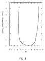
- FIG. 1 is a plot of the solubility of Al(OH) 3 as a function of pH.
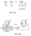
- FIGS. 2A-2B diagrammatically represent the polishing mechanism of the preferred embodiment of the present invention.
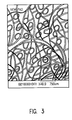
- FIG. 3 shows the surface of a preferred pad for contact chemical reaction polishing.
- FIGS. 2A-B illustrate the mechanism of the preferred embodiment polishing process.
- the silica polishing particle B forms an aluminosilicate AB, upon contact, with hydrated aluminum oxide A on the surface of the workpiece. This reaction occurs because there is a strong specific interaction between the oxides of aluminum and silicon. Both oxides, under suitable circumstances, assume a coordination number of 4 toward oxygen, and both have approximately the same atomic diameter.
- the SiO 2 polishing particle 100 in the slurry is applied to the surface 102 of the aluminum layer 104. Since A, the aluminate ion Al(OH) 4 -1 is geometrically similar to B, Si(OH) 4 , the aluminate ion A can be inserted or exchanged into the SiO 2 polishing particle surface (as represented by the arrow), thus creating an aluminosilicate site AB. AB has a fixed negative charge. Thus, the hydrated aluminum oxide A is removed from the aluminum surface 102 by inserting it (AB) into the top layer of the silica polishing particle 100.
- the spent polishing particle 100 with part of its surface converted to aluminosilicate AB, is discarded and replaced by new silica particles. So, layer-by-layer the surface alumina is removed without scratching the surface 102 or corroding the aluminum 104.
- the silica used in the slurry preferably, has a large surface area, and thus has a small particle size.
- the silica particles are fumed silica, produced by the vapor phase hydrolysis of silicon tetrachloride in a hydrogen oxygen flame. Particles, thus formed, are dispersed in water and neutralized with ammonia or KOH.
- the size of the silica particles should be from 12 to 100 nanometers and preferably, about 30-50 nanometers.
- the silica concentration in the slurry is between 2 and 30 weight percent.
- the pH of the slurry is neutral, between 6-8. An acidic pH prevents formation of the aluminosilicate and an alkaline pH causes aluminum corrosion and recessing. In silica slurries with an acidic pH, i.e., of 3 or less, the aluminum reverts to 6-fold coordination, preventing aluminosilicate formation.
- colloidal silica may be used to polish aluminum alloys.
- Colloidal silica slurries produced by the hydrolysis of alcoxy-silane or by a sol-gel process are equally effective.
- a liner is applied under the aluminum alloy to absorb the oxygen at via interfaces, thereby minimizing stud contact resistance.
- this liner is titanium, but other metals such as Cr, Molybdenum, Ti-W alloy or tungsten may also be used.
- the wafer, with aluminum alloy on top of the liner is heated at a temperature on the order of 500°C. This is called “reflowing" the aluminum. At this temperature, the liner and aluminum form an aluminide; TiAl 3 in case of titanium liner.
- the mechanism of the present invention of polishing with silica slurry is based on the formation of aluminosilicate in the course of polishing. Such aluminosilicate formation only takes place if the hydrated layer forming on the exposed surface of the aluminide intermetallic in the aqueous environment is pure aluminum oxide. Such is the case with TiAl 3 , which is polished by the silica slurry of the present invention.
- the liner is Cr, Mo, Ti-W alloy, or W, and the reflow temperature is above 500°C, then CrAl 13 , MoAl 12 or WAl 12 forms, respectively.
- MoAl 12 oxidizes to Al 2 (MoO 4 ) 3 and, similarly, WAl 12 also oxidizes to a mixed W and Al oxide.
- Neither of these liners form an aluminosilicate and, thus, neither are polished at a fast rate by the silica slurry of the present invention.
- the wafer is heated sufficiently to melt the aluminum so that it flows into recesses and voids forming a relatively uniform layer. This is known as re-flowing the aluminum or reflow.
- areas of conductor arrays on chips are filled with aluminum alloy.
- metal lines are spaced from each other by SiO 2 lines (spaces) of near equal width.
- SiO 2 lines spaces
- the thickness of the surface aluminum layer i.e., above these conductor arrays, is less, by about half the trench depth, than the same layer in the chip's adjacent field areas, i.e., areas where there are no trenches. Because of this thinner aluminum layer in the arrays, polishing according to the present invention clears the aluminum from chip arrays much sooner than from adjacent fields. Thus, overpolishing in the arrays would result in eroding metal lines and narrow SiO 2 spaces. Further, this overpolishing would reduce conductor thickness to increase wire resistance.
- this array overpolishing may be avoided by using a liner in the array of Cr, Mo, W or Ti-W alloy.
- their aluminides are polished slowly enough by the silica slurry to act as polish stops. This is an advantageous characteristic of the preferred embodiment polishing process.
- the alumina on the surface of the aluminum chemically reacts with the surface of the silica polishing particle. Therefore, it is intended that the polishing pad assures contact between the silica polishing particles and the alumina.
- FIG. 3 is a Scanning Electron Microscope (SEM) picture of such a preferred polishing pad.
- SEM Scanning Electron Microscope
- rayon fibers are laid down and held together by a binder.
- the binder is preferably, an acrylic-butadien rubber copolymer.
- the laid-down fibers create tracks, like those of a bobsled run, wherein the slurry particles roll around upon shear from the pad, thereby providing a maximum surface contact between the polishing particles and the alumina surface. Because of the openness of this pad structure, slurry particles are not pressed into the aluminum surface and, therefore, only mild mechanical abrasion takes place.
- the pad surface geometry insures a contact-chemical reaction between the polishing particles and the surface to be polished.
- polishing pads are, for example, napped poromeric synthetics such as a polyurethane foam with a vertically oriented pore structure.
- the backing is preferably soft and thin, to prevent scratches and reduce dishing.
- Two such backings are mylar and felt.
- Examples of such alternate preferred embodiment pads are the DF200II (which has a mylar backing) and Meritex (which is felt-backed) polyurethane pads, both from Rodel.
- Eight inch diameter patterned aluminum films were polished on a Westech 372 polishing machine.
- the pad used was that in FIG. 3.
- a down force of 6 psi was applied to the pad.
- the platen speed was 100 rpm and the carrier speed was 10 rpm.
- the resulting aluminum polishing rate was 150 nanometers per minute.
- the SiO 2 removal rate was 10 nanometers per minute.
- the resulting polished surface was free of scratches, corrosion and chemical recesses. Electrical testing of the polished work piece detected no unwanted opens or shorts.
Landscapes
- Mechanical Treatment Of Semiconductor (AREA)
- Finish Polishing, Edge Sharpening, And Grinding By Specific Grinding Devices (AREA)
Applications Claiming Priority (2)
| Application Number | Priority Date | Filing Date | Title |
|---|---|---|---|
| US572362 | 1984-01-20 | ||
| US57236295A | 1995-12-14 | 1995-12-14 |
Publications (2)
| Publication Number | Publication Date |
|---|---|
| EP0779655A2 true EP0779655A2 (fr) | 1997-06-18 |
| EP0779655A3 EP0779655A3 (fr) | 1997-07-16 |
Family
ID=24287465
Family Applications (1)
| Application Number | Title | Priority Date | Filing Date |
|---|---|---|---|
| EP96307792A Withdrawn EP0779655A3 (fr) | 1995-12-14 | 1996-10-29 | Procédé pour le polissage chimique-mécanique d'un substrat d'un composant électronique |
Country Status (3)
| Country | Link |
|---|---|
| US (1) | US5752875A (fr) |
| EP (1) | EP0779655A3 (fr) |
| JP (1) | JP3118195B2 (fr) |
Cited By (1)
| Publication number | Priority date | Publication date | Assignee | Title |
|---|---|---|---|---|
| EP1029907A1 (fr) * | 1999-02-18 | 2000-08-23 | Clariant (France) S.A. | Procédé de polissage mécano-chimique de une couche en un matériau conducteur d'aluminium ou d'alliage d'aluminium |
Families Citing this family (15)
| Publication number | Priority date | Publication date | Assignee | Title |
|---|---|---|---|---|
| JPH09115866A (ja) * | 1995-10-17 | 1997-05-02 | Mitsubishi Electric Corp | 半導体装置の製造方法 |
| US5769691A (en) * | 1996-06-14 | 1998-06-23 | Speedfam Corp | Methods and apparatus for the chemical mechanical planarization of electronic devices |
| US5897426A (en) * | 1998-04-24 | 1999-04-27 | Applied Materials, Inc. | Chemical mechanical polishing with multiple polishing pads |
| JP3516157B2 (ja) * | 1998-12-14 | 2004-04-05 | 松下電器産業株式会社 | 化学的機械研磨用研磨液および研磨方法 |
| US6258711B1 (en) * | 1999-04-19 | 2001-07-10 | Speedfam-Ipec Corporation | Sacrificial deposit to improve damascene pattern planarization in semiconductor wafers |
| US6509269B2 (en) | 1999-10-19 | 2003-01-21 | Applied Materials, Inc. | Elimination of pad glazing for Al CMP |
| US6350393B2 (en) * | 1999-11-04 | 2002-02-26 | Cabot Microelectronics Corporation | Use of CsOH in a dielectric CMP slurry |
| US20040192178A1 (en) * | 2003-03-28 | 2004-09-30 | Barak Yardeni | Diamond conditioning of soft chemical mechanical planarization/polishing (CMP) polishing pads |
| US20060118760A1 (en) * | 2004-12-03 | 2006-06-08 | Yang Andy C | Slurry composition and methods for chemical mechanical polishing |
| DE102007035266B4 (de) * | 2007-07-27 | 2010-03-25 | Siltronic Ag | Verfahren zum Polieren eines Substrates aus Silicium oder einer Legierung aus Silicium und Germanium |
| KR20130090209A (ko) * | 2012-02-03 | 2013-08-13 | 삼성전자주식회사 | 기판처리장치 및 기판처리방법 |
| US9238295B2 (en) | 2013-05-31 | 2016-01-19 | Rohm And Haas Electronic Materials Cmp Holdings, Inc. | Soft and conditionable chemical mechanical window polishing pad |
| US9238296B2 (en) | 2013-05-31 | 2016-01-19 | Rohm And Haas Electronic Materials Cmp Holdings, Inc. | Multilayer chemical mechanical polishing pad stack with soft and conditionable polishing layer |
| US9233451B2 (en) | 2013-05-31 | 2016-01-12 | Rohm And Haas Electronic Materials Cmp Holdings, Inc. | Soft and conditionable chemical mechanical polishing pad stack |
| US9102034B2 (en) | 2013-08-30 | 2015-08-11 | Rohm And Haas Electronic Materials Cmp Holdings, Inc. | Method of chemical mechanical polishing a substrate |
Family Cites Families (34)
| Publication number | Priority date | Publication date | Assignee | Title |
|---|---|---|---|---|
| US4132037A (en) * | 1977-02-28 | 1979-01-02 | Siltec Corporation | Apparatus for polishing semiconductor wafers |
| US4376148A (en) * | 1980-09-18 | 1983-03-08 | Norwood Industries, Inc. | Impregnated non-woven sheet material with ionically solubilized resin |
| JPS5845861A (ja) * | 1981-09-09 | 1983-03-17 | Hitachi Ltd | 表面加工用ポリシヤ |
| US4944836A (en) * | 1985-10-28 | 1990-07-31 | International Business Machines Corporation | Chem-mech polishing method for producing coplanar metal/insulator films on a substrate |
| US4789648A (en) * | 1985-10-28 | 1988-12-06 | International Business Machines Corporation | Method for producing coplanar multi-level metal/insulator films on a substrate and for forming patterned conductive lines simultaneously with stud vias |
| US4841680A (en) * | 1987-08-25 | 1989-06-27 | Rodel, Inc. | Inverted cell pad material for grinding, lapping, shaping and polishing |
| US4879258A (en) * | 1988-08-31 | 1989-11-07 | Texas Instruments Incorporated | Integrated circuit planarization by mechanical polishing |
| US4910155A (en) * | 1988-10-28 | 1990-03-20 | International Business Machines Corporation | Wafer flood polishing |
| US5352277A (en) * | 1988-12-12 | 1994-10-04 | E. I. Du Pont De Nemours & Company | Final polishing composition |
| US5396737B1 (en) * | 1989-01-18 | 1997-12-23 | Minnesota Mining & Mfg | Compound glazing or polishing pad |
| US5007128B1 (en) * | 1989-01-18 | 1993-12-07 | Minnesota Mining And Manufacturing Company | Compounding,glazing or polishing pad |
| US5185964A (en) * | 1989-01-18 | 1993-02-16 | Minnesota Mining And Manufacturing Company | Compounding, glazing or polishing pad |
| US4962562A (en) * | 1989-01-18 | 1990-10-16 | Minnesota Mining And Manufacturing Company | Compounding, glazing or polishing pad |
| US5084071A (en) * | 1989-03-07 | 1992-01-28 | International Business Machines Corporation | Method of chemical-mechanical polishing an electronic component substrate and polishing slurry therefor |
| US4959113C1 (en) * | 1989-07-31 | 2001-03-13 | Rodel Inc | Method and composition for polishing metal surfaces |
| US5228886A (en) * | 1990-10-09 | 1993-07-20 | Buehler, Ltd. | Mechanochemical polishing abrasive |
| JP3290189B2 (ja) * | 1991-04-11 | 2002-06-10 | 旭電化工業株式会社 | シリコンウェハーの研磨方法 |
| JPH0529288A (ja) * | 1991-07-18 | 1993-02-05 | Mitsubishi Materials Corp | 化合物半導体ウエハの研磨方法 |
| US5287663A (en) * | 1992-01-21 | 1994-02-22 | National Semiconductor Corporation | Polishing pad and method for polishing semiconductor wafers |
| US5245790A (en) * | 1992-02-14 | 1993-09-21 | Lsi Logic Corporation | Ultrasonic energy enhanced chemi-mechanical polishing of silicon wafers |
| US5264010A (en) * | 1992-04-27 | 1993-11-23 | Rodel, Inc. | Compositions and methods for polishing and planarizing surfaces |
| US5302551A (en) * | 1992-05-11 | 1994-04-12 | National Semiconductor Corporation | Method for planarizing the surface of an integrated circuit over a metal interconnect layer |
| US5209816A (en) * | 1992-06-04 | 1993-05-11 | Micron Technology, Inc. | Method of chemical mechanical polishing aluminum containing metal layers and slurry for chemical mechanical polishing |
| US5328553A (en) * | 1993-02-02 | 1994-07-12 | Motorola Inc. | Method for fabricating a semiconductor device having a planar surface |
| US5407526A (en) * | 1993-06-30 | 1995-04-18 | Intel Corporation | Chemical mechanical polishing slurry delivery and mixing system |
| US5340370A (en) * | 1993-11-03 | 1994-08-23 | Intel Corporation | Slurries for chemical mechanical polishing |
| JP2900777B2 (ja) * | 1993-12-14 | 1999-06-02 | 信越半導体株式会社 | 研磨部材およびウエーハ研磨装置 |
| JPH07221168A (ja) * | 1994-02-02 | 1995-08-18 | Toto Ltd | 静電チャックの表面研磨方法 |
| JP3441142B2 (ja) * | 1994-02-04 | 2003-08-25 | 日産化学工業株式会社 | 半導体ウェーハーの研磨方法 |
| JP3313505B2 (ja) * | 1994-04-14 | 2002-08-12 | 株式会社日立製作所 | 研磨加工法 |
| JP2894208B2 (ja) * | 1994-06-02 | 1999-05-24 | 信越半導体株式会社 | シリコンウェーハ研磨用研磨剤及び研磨方法 |
| US5534106A (en) * | 1994-07-26 | 1996-07-09 | Kabushiki Kaisha Toshiba | Apparatus for processing semiconductor wafers |
| US5527423A (en) * | 1994-10-06 | 1996-06-18 | Cabot Corporation | Chemical mechanical polishing slurry for metal layers |
| US5486265A (en) * | 1995-02-06 | 1996-01-23 | Advanced Micro Devices, Inc. | Chemical-mechanical polishing of thin materials using a pulse polishing technique |
-
1996
- 1996-10-29 EP EP96307792A patent/EP0779655A3/fr not_active Withdrawn
- 1996-11-11 JP JP29856796A patent/JP3118195B2/ja not_active Expired - Fee Related
-
1997
- 1997-07-09 US US08/890,457 patent/US5752875A/en not_active Expired - Fee Related
Non-Patent Citations (1)
| Title |
|---|
| None |
Cited By (4)
| Publication number | Priority date | Publication date | Assignee | Title |
|---|---|---|---|---|
| EP1029907A1 (fr) * | 1999-02-18 | 2000-08-23 | Clariant (France) S.A. | Procédé de polissage mécano-chimique de une couche en un matériau conducteur d'aluminium ou d'alliage d'aluminium |
| FR2789998A1 (fr) * | 1999-02-18 | 2000-08-25 | Clariant France Sa | Nouvelle composition de polissage mecano-chimique d'une couche en un materiau conducteur d'aluminium ou d'alliage d'aluminium |
| US6386950B1 (en) | 1999-02-18 | 2002-05-14 | Clariant (France) S.A. | Process for mechanical chemical polishing of layer of aluminium or aluminium alloy conducting material |
| SG97841A1 (en) * | 1999-02-18 | 2003-08-20 | Clariant Finance Bvi Ltd | Process for mechanical chemical polishing of a layer of aluminium or aluminium alloy conducting material |
Also Published As
| Publication number | Publication date |
|---|---|
| US5752875A (en) | 1998-05-19 |
| EP0779655A3 (fr) | 1997-07-16 |
| JP3118195B2 (ja) | 2000-12-18 |
| JPH09174419A (ja) | 1997-07-08 |
Similar Documents
| Publication | Publication Date | Title |
|---|---|---|
| US5752875A (en) | Method of chemically-mechanically polishing an electronic component | |
| KR100214749B1 (ko) | 동계 금속용 연마액 및 반도체장치의 제조방법 | |
| US7104869B2 (en) | Barrier removal at low polish pressure | |
| KR100505860B1 (ko) | 금속막 제거용 평탄화 조성물 | |
| KR100351655B1 (ko) | 구리 또는 구리 합금 집적 회로 금속화 층을 연마하기 위한 화학적-기계적 평탄화 슬러리 | |
| KR100348097B1 (ko) | 폴리싱방법, 반도체장치의 제조방법 및 반도체제조장치 | |
| US7060606B2 (en) | Method and apparatus for chemical mechanical polishing of semiconductor substrates | |
| KR100508838B1 (ko) | 반도체 장치의 제조 방법 및 그의 연마액 | |
| CA1245517A (fr) | Methode de polissage chimico-mecanique pour la production de depots coplanaires metal/isolant sur un substrat | |
| WO2002044293A2 (fr) | Procede et composition permettant d'eliminer les materiaux residuels lors de la planarisation d'un substrat | |
| EP1147546A1 (fr) | Procede de diminution de la vitesse de creusage pendant le processus de planarisation chimico-mecanique de structures a semi-conducteurs metalliques | |
| KR100578596B1 (ko) | 화학기계적 연마용 슬러리 조성물, 이를 이용한반도체소자의 표면 평탄화 방법 및 슬러리 조성물의선택비 제어방법 | |
| KR20000028886A (ko) | 구리를 기초로 한 금속 연마 조성물 및 반도체장치의제조방법 | |
| JP3668046B2 (ja) | 研磨布及びこの研磨布を用いた半導体装置の製造方法 | |
| KR20080028790A (ko) | 텅스텐 배선 형성용 슬러리 조성물 및 이를 이용한 반도체소자의 제조 방법 | |
| US20020173221A1 (en) | Method and apparatus for two-step polishing | |
| US6530824B2 (en) | Method and composition for polishing by CMP | |
| EP0982766B1 (fr) | Procédé de polissage mécano-chimique d'une couche d'un matériau à base de cuivre | |
| US6114215A (en) | Generating non-planar topology on the surface of planar and near-planar substrates | |
| JP2001205554A (ja) | 研磨装置 | |
| JP2002064070A (ja) | 化学機械研磨方法および化学機械研磨用スラリ組成物 | |
| US6458016B2 (en) | Polishing fluid, polishing method, semiconductor device and semiconductor device fabrication method | |
| US20020125460A1 (en) | Compositions for chemical mechanical planarization of tungsten | |
| US6439972B2 (en) | Polishing fluid, polishing method, semiconductor device and semiconductor device fabrication method | |
| US20030124861A1 (en) | Method for manufacturing metal line contact plug semiconductor device |
Legal Events
| Date | Code | Title | Description |
|---|---|---|---|
| PUAI | Public reference made under article 153(3) epc to a published international application that has entered the european phase |
Free format text: ORIGINAL CODE: 0009012 |
|
| PUAL | Search report despatched |
Free format text: ORIGINAL CODE: 0009013 |
|
| AK | Designated contracting states |
Kind code of ref document: A2 Designated state(s): DE FR GB |
|
| AK | Designated contracting states |
Kind code of ref document: A3 Designated state(s): DE FR GB |
|
| 17P | Request for examination filed |
Effective date: 19980112 |
|
| 17Q | First examination report despatched |
Effective date: 20011203 |
|
| STAA | Information on the status of an ep patent application or granted ep patent |
Free format text: STATUS: THE APPLICATION IS DEEMED TO BE WITHDRAWN |
|
| 18D | Application deemed to be withdrawn |
Effective date: 20020416 |