EP0779659A2 - Circuit intégré semi-conducteur - Google Patents
Circuit intégré semi-conducteur Download PDFInfo
- Publication number
- EP0779659A2 EP0779659A2 EP96119726A EP96119726A EP0779659A2 EP 0779659 A2 EP0779659 A2 EP 0779659A2 EP 96119726 A EP96119726 A EP 96119726A EP 96119726 A EP96119726 A EP 96119726A EP 0779659 A2 EP0779659 A2 EP 0779659A2
- Authority
- EP
- European Patent Office
- Prior art keywords
- speed operation
- high speed
- circuit section
- operation circuit
- semiconductor integrated
- Prior art date
- Legal status (The legal status is an assumption and is not a legal conclusion. Google has not performed a legal analysis and makes no representation as to the accuracy of the status listed.)
- Withdrawn
Links
- 239000004065 semiconductor Substances 0.000 title claims abstract description 50
- 230000003071 parasitic effect Effects 0.000 claims abstract description 15
- 238000010586 diagram Methods 0.000 description 13
- 230000002411 adverse Effects 0.000 description 6
- 238000000034 method Methods 0.000 description 6
- 239000000470 constituent Substances 0.000 description 5
- 230000000694 effects Effects 0.000 description 5
- 238000006243 chemical reaction Methods 0.000 description 4
- 230000036039 immunity Effects 0.000 description 3
- 238000010276 construction Methods 0.000 description 1
- 230000006866 deterioration Effects 0.000 description 1
- 230000010354 integration Effects 0.000 description 1
- 230000035945 sensitivity Effects 0.000 description 1
- 238000001228 spectrum Methods 0.000 description 1
- 239000000758 substrate Substances 0.000 description 1
Images



Classifications
-
- H—ELECTRICITY
- H10—SEMICONDUCTOR DEVICES; ELECTRIC SOLID-STATE DEVICES NOT OTHERWISE PROVIDED FOR
- H10D—INORGANIC ELECTRIC SEMICONDUCTOR DEVICES
- H10D89/00—Aspects of integrated devices not covered by groups H10D84/00 - H10D88/00
- H10D89/10—Integrated device layouts
Definitions
- the present invention relates to semiconductor integrated circuits in which the electromagnetic irradiation generated is reduced, and more particularly to semiconductor integrated circuits in which the electromagnetic irradiation resulting from the on-off operation of transistor elements is reduced.
- transistor elements thereof are sources of electromagnetic irradiation due to high frequency components in the rise and fall times of their high speed on-off operation.
- the electromagnetic irradiation causes electromagnetic interference problems in nearby circuits and equipment, thus giving rise to performance deterioration and erroneous operation of these circuits and equipment.
- Fig. 1 shows a circuit for processing a serial signal by converting it into parallel data signals.
- an S/P (serial-parallel) converter 11 converts a serial data signal inputted at frequency f from a data input terminal IN into n parallel data according to the output of a clock n-divider 14 that divides by n the clock signal inputted from a clock input terminal C, and outputs a sequence of n-parallel data 1 - n of frequency f/n.
- a digital signal processor 12 executes predetermined processing on the n parallel data.
- a P/S (parallel-serial) converter 13 converts the n parallel data having been processed in the digital signal processor 12 into a serial signal, and outputs it as data of frequency f from a data output terminal OUT.
- the above data processing circuit comprises MOS transistors, for instance, as its semiconductor elements which are all designed so as to drive their gate at a maximum operating frequency. This means that the rise and fall times of the MOS transistors are extremely short, thus giving rise to high frequency wave generation and electromagnetic wave irradiation as described above.
- Techniques for reducing such electromagnetic irradiation have been proposed in, for instance, Japanese Patent Application Kokai Publication No. Sho 64-15820 and Japanese Patent Application Kokai Publication No. Hei 3-129416.
- a circuit generates a clock frequency that is necessary for its own operation from a clock inputted at a frequency lower than the necessary high clock frequency, thus reducing electromagnetic irradiation unlike the case where the high clock frequency is inputted to an input section.
- EMI electromagnetic interference
- EMS electromagnetic susceptibility
- Fig. 2 illustrates an example of processing of a serial signal by converting the same signal into parallel data.
- the S/P converter 11 converts a serial data signal inputted at frequency f from a data input terminal IN into n parallel data according to the output of a clock n-divider 14 that divides by n the clock signal inputted from a clock input terminal C, and outputs a sequence of n-parallel data 1 - n of frequency f/n.
- the digital signal processor 12 executes the predetermined processing on the n parallel data.
- the P/S converter 13 converts the n parallel data having been processed in the digital signal processor 12 into the serial signal, and outputs it as data of frequency f from the data output terminal OUT.
- the P/S converter 13 further has an output control signal input terminal S and, when a control signal is outputted therefrom, it ceases the output of data from the output terminal OUT.
- the semiconductor integrated circuits which are obtainable according to the disclosed techniques require such additional components as a frequency converter and a waveform shaper. These additional circuit components increase the scale of the circuit and are therefore undesired for realizing a small size and high integration density semiconductor integrated circuit.
- the second problem in the disclosed techniques is the sensitivity to external noise, giving rise to erroneous operations. This is so because the element transistors have a high cut-off frequency and are therefore sensitive to high frequency noise as well.
- An object of the invention is to provide a semiconductor integrated circuit which enables the effective reduction of the electromagnetic irradiation in its circuit sections and is also highly immune to noise.
- a semiconductor integrated circuit comprising:
- the electromagnetic irradiation from such elements as MOS transistors and bipolar transistors is inversely proportional to the rise and fall times of signals, that is, it is increased with increasing speed of operation.
- the circuit sections requiring a high frequency have to be realized such that they drive their gates with short signal rise and fall times
- the electromagnetic irradiation in at least circuit sections requiring a low frequency can be reduced by constructing these circuit sections with element transistors, which are driven with increased signal rise and fall times by increasing the channel length or reducing the bias voltage or increasing the output capacitance (i.e., parasitic capacitance).
- the elements have a low cut-off frequency and hence is less sensitive to noise, and it is possible to provide a semiconductor integrated circuit which has increased immunity to noise.
- a first embodiment of the invention concerns a circuit for processing a data signal by making the serial-parallel conversion thereof.
- the S/P converter 11 shown in Fig. 1 converts the serial data signal inputted at frequency f from the data signal input terminal IN into n parallel data, and outputs a sequence of n-parallel data 1 - n of frequency f/n.
- the clock n-divider 14 divides the clock signal from the clock input terminal C by n and inputs the resultant signal to the S/P converter 11 for the conversion of the serial signal to the parallel data.
- the digital signal processor 12 executes the predetermined processing on the n parallel data.
- the P/S converter 13 converts the n parallel data having been processed in the digital signal processor 12 into the serial signal, and outputs it as data of frequency f which is outputted from the data output terminal OUT.
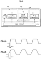
- Fig. 3 is a block diagram showing the circuit shown in Fig. 1, which is fabricated as a semiconductor integrated circuit on a semiconductor substrate 100.
- a short channel element region 101 which constitutes the S/P converter 11, the P/S converter 13 and the clock n-divider (i.e., 1/n divider) 14, has its elements fabricated as short channel MOS transistors capable of operating at a high speed with short rise and fall times.
- a long channel element region 102 which constitutes the digital signal processor 12, has its elements fabricated as long channel MOS transistors operable with long rise and fall times because these elements are operated at a relatively low speed corresponding to the frequency f/n.
- a bias circuit 15 supplies a bias to the circuit sections described above.
- the S/P converter 11, P/S converter 13 and clock n-divider 14 are operated in a state with as short rise and fall times as approximately 1 ns, as shown in Fig. 4A, because of the short channel of their constituent MOS transistors.
- the digital signal processor 12 is operated with longer rise and fall times of approximately 3 ns, as shown in Fig. 4B, because of the longer channel of its constituent MOS transistors. In this case, the digital signal processor 12 is operated at frequency f/n, and its operation is not adversely affected by the longer rise and fall times.
- the digital signal processor 12 constitutes a major part of the semiconductor integrated circuit, and it is constructed with the long channel MOS transistors so that it is possible to increase the rise and fall times for these MOS transistors without resultant adverse effects on its operation.
- the electromagnetic irradiation accompanying the MOS transistor operation is inversely proportional to the rise and fall times, and this means that it is possible to reduce the electromagnetic irradiation in the digital signal processor 12.
- the rise and fall times are increased from 1 ns to 3 ns for the digital signal processor 12 to obtain corresponding electromagnetic irradiation reduction therein.
- Fig. 5 is a block diagram similar to Fig. 3 but showing the second embodiment of the invention applied again to the circuit shown in Fig. 1.
- the S/P converter 11, the digital signal processor 12, the P/S converter 13 and the clock n-divider (i.e., 1/n divider) 14 are constructed with elements having the same structure, for instance, MOS transistors having the same channel length, and the embodiment further comprises a high voltage bias circuit 15A and a low voltage bias circuit 15B.
- the high voltage bias circuit 15A applies a high voltage as gate-drain bias to the MOS transistors of the S/P converter 11, P/S converter 13 and clock n-divider 14 to permit high speed operation thereof with short rise and fall times corresponding to frequency f.
- the low voltage bias circuit 15B applies a low voltage as gate-drain bias to the MOS transistors of the digital signal processor 12 to increase the rise and fall times for operation at a relatively low speed corresponding to frequency f/n.
- the S/P converter 11, P/S converter 13 and clock n-divider 14 are operated in a state with as short rise and fall times as approximately 1 ns as shown in Fig. 4A since the high voltage bias is supplied to their MOS transistors.
- the digital signal processor 12 is operated in a state with longer rise and fall times of approximately 3 ns, as shown in Fig. 4B, since the low voltage bias is supplied to its MOS transistors.
- the digital signal processor 12 constitutes a major part of the semiconductor integrated circuit, so that it is possible to increase the rise and fall times for the digital signal processor 12 without resultant adverse effects on the operation. This means that it is possible to reduce the electromagnetic irradiation in the digital signal processor 12 constituting a major part of the circuit. Even though electromagnetic irradiation is generated as in the prior art in other circuit sections, i.e., the S/P converter 11, P/S converter 13 and clock n-divider 14, the electromagnetic irradiation generated in the overall semiconductor integrated circuit is remarkably reduced because these other circuit sections together constitute only a small proportion of the circuit.
- first and second embodiments relate to the application of the invention to the semiconductor integrated circuit which is for serial-parallel conversion and for carrying out digital signal processing
- the invention is generally applicable to any semiconductor integrated circuit having a high speed operation circuit section and a low speed operation circuit section.
- Fig. 6 is a block diagram showing the third embodiment, the block diagram corresponding to that of Fig. 3 for the first embodiment in which the present invention is applied to the circuit shown in Fig. 1.
- a low capacitance (parasitic capacitance) region 101' which constitutes the S/P converter 11, the P/S converter 13 and the clock n-divider (i.e., 1/n divider) 14, has its elements fabricated as low output capacitance (parasitic capacitance), high cut-off frequency MOS transistors capable of operating at a high speed with short rise and fall times corresponding to frequency f.
- a bias circuit 15 is provided for supplying a bias to the various circuit sections mentioned above.
- the S/P converter 11, P/S converter 13 and clock n-divider 14 are operated in a state with as short rise and fall times as approximately 1 ns, as shown in Fig. 7A, because of the low output capacitance (parasitic capacitance) of their constituent MOS transistors.
- the digital signal processor 12 is operated with longer rise and fall times of approximately 5 ns, as shown in Fig. 7B, because of the higher output capacitance (parasitic capacitance) of its constituent MOS transistors. In this case, the digital signal processor 12 is operated at frequency f/n, and its operation is not adversely affected by the longer rise and fall times.
- the digital signal processor 12 which is constructed with the high Output capacitance (parasitic capacitance) MOS transistors, so that it is possible to increase the rise and fall times for these MOS transistors without resultant adverse effects on operation.
- the digital signal processor 12 which is constructed with the high Output capacitance (parasitic capacitance) MOS transistors, so that it is possible to increase the rise and fall times for these MOS transistors without resultant adverse effects on operation.
- the electromagnetic irradiation accompanying the MOS transistor operation is inversely proportional to the rise and fall times, which means the possibility of reducing the electromagnetic irradiation in the digital signal processor 12.
- the rise and fall times are increased from 1 ns to 5 ns to obtain corresponding electromagnetic irradiation reduction, as will be seen from the following calculation.
- Equation 1 is given as a trapezoidal wave equation.
- I is the peak to peak value
- d is the duty cycle
- tr is the rise and fall times
- T is the cycle period
- n is the harmonic degree.
- the eleventh harmonic is given as the following equation 2.
- the equation 3 means that the irradiation is reduced by 58% (or 4.7 dB) compared to the irradiation given by the equation 2.
- Fig. 8 is a graph showing the trapezoidal wave envelope curves in the cases of Figs. 7A and 7B. As will be seen from Fig. 8, the higher the harmonic degree, the electromagnetic irradiation is reduced more with increasing rise and fall times.
- Fig. 9 is a block diagram showing a fourth embodiment of the invention.
- the output of the P/S converter 13 is turned on-off according to a signal from the output control signal input terminal S.
- the remaining portions are the same as those in Fig. 1.
- Immunity to noise can be reduced, that is, erroneous operations due to noise can be reduced, by using a low cut-off frequency, high capacitance (parasitic capacitance) transistor as an element constituting the output control signal input terminal S.
- This fourth embodiment can be applied to the second and third embodiments shown in Figs. 5 and 6.
- Fig. 10 shows an example of the pin location in a semiconductor integrated circuit having both high frequency signal elements and low frequency signal elements.
- the high frequency signal elements are located as close as possible (at a periphery portion) to the high frequency signal input and output terminals (or pins) to make high frequency signal current loops as short as possible. By so doing, it is possible to reduce electromagnetic irradiation due to the high frequency signals, which is the most serious problem in the electromagnetic irradiation.
- reference numeral 601 designates the input and output pins
- reference numeral 602 designates inter-connections.
- the above third and fourth embodiments also relate to the application of the invention to a semiconductor integrated circuit which is for serial-parallel conversion and for carrying out digital signal processing
- the invention is generally applicable to any semiconductor integrated circuit having a high speed operation circuit section and a low speed operation circuit section.
- the invention is also applicable to other semiconductor integrated circuit, for instance using bipolar transistors.
- the low speed operation circuit section is constructed with long rise and fall time elements.
- the electromagnetic irradiation is thus reduced at least in the low speed operation circuit section constructed with the longer rise and fall time elements, although the high speed operation circuit section has to be realized with the short rise and fall time gates.
- the low speed operation circuit section elements with MOS transistors each having a longer channel than high speed operation circuit section MOS transistors, it is possible to suppress the electromagnetic irradiation from the low speed operation circuit section with longer MOS transistor rise and fall times thereof.
- the bias voltage supplied to the low speed operation circuit section elements is lower than the bias voltage supplied to the high speed operation circuit section elements, it is possible to provide longer rise and fall times for the MOS transistors in the low speed operation circuit section and suppress the electromagnetic irradiation therefrom.
- the low speed operation circuit section elements with MOS transistors having a higher capacitance (parasitic capacitance) of the high speed operation circuit section MOS transistors, it is possible to provide longer rise and fall times for the MOS transistors in the low speed operation circuit section and suppress the electromagnetic irradiation therefrom.
Landscapes
- Semiconductor Integrated Circuits (AREA)
- Logic Circuits (AREA)
Applications Claiming Priority (2)
| Application Number | Priority Date | Filing Date | Title |
|---|---|---|---|
| JP327176/95 | 1995-12-15 | ||
| JP7327176A JP2770851B2 (ja) | 1994-12-15 | 1995-12-15 | 半導体集積回路 |
Publications (2)
| Publication Number | Publication Date |
|---|---|
| EP0779659A2 true EP0779659A2 (fr) | 1997-06-18 |
| EP0779659A3 EP0779659A3 (fr) | 1998-07-08 |
Family
ID=18196164
Family Applications (1)
| Application Number | Title | Priority Date | Filing Date |
|---|---|---|---|
| EP96119726A Withdrawn EP0779659A3 (fr) | 1995-12-15 | 1996-12-09 | Circuit intégré semi-conducteur |
Country Status (1)
| Country | Link |
|---|---|
| EP (1) | EP0779659A3 (fr) |
Citations (2)
| Publication number | Priority date | Publication date | Assignee | Title |
|---|---|---|---|---|
| JPS6415820A (en) | 1987-07-10 | 1989-01-19 | Hitachi Ltd | Integrated circuit |
| JPH03129416A (ja) | 1989-10-14 | 1991-06-03 | Hitachi Ltd | パルス供給方式、集積回路および情報処理装置 |
Family Cites Families (4)
| Publication number | Priority date | Publication date | Assignee | Title |
|---|---|---|---|---|
| JPS5472691A (en) * | 1977-11-21 | 1979-06-11 | Toshiba Corp | Semiconductor device |
| EP0119689A3 (fr) * | 1983-02-22 | 1986-11-20 | Northern Telecom Limited | Dispositif d'interface en série et en parallèle |
| US5134702A (en) * | 1986-04-21 | 1992-07-28 | Ncr Corporation | Serial-to-parallel and parallel-to-serial converter |
| US5287536A (en) * | 1990-04-23 | 1994-02-15 | Texas Instruments Incorporated | Nonvolatile memory array wordline driver circuit with voltage translator circuit |
-
1996
- 1996-12-09 EP EP96119726A patent/EP0779659A3/fr not_active Withdrawn
Patent Citations (2)
| Publication number | Priority date | Publication date | Assignee | Title |
|---|---|---|---|---|
| JPS6415820A (en) | 1987-07-10 | 1989-01-19 | Hitachi Ltd | Integrated circuit |
| JPH03129416A (ja) | 1989-10-14 | 1991-06-03 | Hitachi Ltd | パルス供給方式、集積回路および情報処理装置 |
Also Published As
| Publication number | Publication date |
|---|---|
| EP0779659A3 (fr) | 1998-07-08 |
Similar Documents
| Publication | Publication Date | Title |
|---|---|---|
| US5418476A (en) | Low voltage output buffer with improved speed | |
| US6211715B1 (en) | Semiconductor integrated circuit incorporating therein clock supply circuit | |
| US7138852B2 (en) | Semiconductor integrated circuit device | |
| US6608515B2 (en) | Bus agent utilizing dynamic biasing circuitry to translate a signal to a core voltage level | |
| JPH045289B2 (fr) | ||
| JPH0514167A (ja) | 出力ドライバ回路 | |
| EP0779659A2 (fr) | Circuit intégré semi-conducteur | |
| US6023183A (en) | Voltage conversion circuit and method | |
| JP2605565B2 (ja) | 半導体集積回路 | |
| US5343099A (en) | Output device capable of high speed operation and operating method thereof | |
| EP0782269A3 (fr) | Circuit intégré semi-conducteur | |
| Yang et al. | Design for velocity saturated, short-channel CMOS drivers with simultaneous switching noise and switching time considerations | |
| KR20010040990A (ko) | 과전압 보호 i/o 버퍼 | |
| KR100233186B1 (ko) | 전자기 방사가 감소된 반도체 장치 | |
| US4961012A (en) | Semiconductor integrated circuit device responsive to clock signals having different amplitudes | |
| JP2770851B2 (ja) | 半導体集積回路 | |
| US5774015A (en) | Compact semiconductor integrated circuit capable of reducing electromagnetic emission | |
| EP0720294B1 (fr) | Circuit d'interface pour dispositifs électroniques intégrés monolithiquement sur un semi-conducteur par la technologie MOS/CMOS | |
| EP0249040A2 (fr) | Circuit de conversion selon Booth | |
| JP2871309B2 (ja) | 電源電圧検知回路 | |
| EP0480681A1 (fr) | Circuit intégré à semi-conducteurs | |
| JP2565083B2 (ja) | トライステートバスプルアップ回路 | |
| EP0284936A2 (fr) | Cellule compatible TTL pour circuits integrés CMOS | |
| US6215341B1 (en) | Deceleration circuit | |
| JPH05291914A (ja) | Mosドライバー段の作動特性最適化装置 |
Legal Events
| Date | Code | Title | Description |
|---|---|---|---|
| PUAI | Public reference made under article 153(3) epc to a published international application that has entered the european phase |
Free format text: ORIGINAL CODE: 0009012 |
|
| AK | Designated contracting states |
Kind code of ref document: A2 Designated state(s): DE FR GB |
|
| PUAL | Search report despatched |
Free format text: ORIGINAL CODE: 0009013 |
|
| AK | Designated contracting states |
Kind code of ref document: A3 Designated state(s): DE FR GB |
|
| 17P | Request for examination filed |
Effective date: 19980805 |
|
| 17Q | First examination report despatched |
Effective date: 20021029 |
|
| STAA | Information on the status of an ep patent application or granted ep patent |
Free format text: STATUS: THE APPLICATION IS DEEMED TO BE WITHDRAWN |
|
| 18D | Application deemed to be withdrawn |
Effective date: 20030611 |