EP0779688A1 - Circuit d'alimentation pour un laser à diode - Google Patents
Circuit d'alimentation pour un laser à diode Download PDFInfo
- Publication number
- EP0779688A1 EP0779688A1 EP96309032A EP96309032A EP0779688A1 EP 0779688 A1 EP0779688 A1 EP 0779688A1 EP 96309032 A EP96309032 A EP 96309032A EP 96309032 A EP96309032 A EP 96309032A EP 0779688 A1 EP0779688 A1 EP 0779688A1
- Authority
- EP
- European Patent Office
- Prior art keywords
- laser diode
- npn transistor
- base
- anode
- input data
- Prior art date
- Legal status (The legal status is an assumption and is not a legal conclusion. Google has not performed a legal analysis and makes no representation as to the accuracy of the status listed.)
- Granted
Links
Images


Classifications
-
- H—ELECTRICITY
- H01—ELECTRIC ELEMENTS
- H01S—DEVICES USING THE PROCESS OF LIGHT AMPLIFICATION BY STIMULATED EMISSION OF RADIATION [LASER] TO AMPLIFY OR GENERATE LIGHT; DEVICES USING STIMULATED EMISSION OF ELECTROMAGNETIC RADIATION IN WAVE RANGES OTHER THAN OPTICAL
- H01S5/00—Semiconductor lasers
- H01S5/04—Processes or apparatus for excitation, e.g. pumping, e.g. by electron beams
- H01S5/042—Electrical excitation ; Circuits therefor
Definitions
- the present invention relates to a laser diode driving circuit used in an optical disk device or the like.
- a laser light source generally, a laser diode is used.
- Two types of laser diodes are available: one grounded at the cathode side and the other grounded at the anode side.
- An example of the conventional driving circuit for the laser diode grounded at the cathode side is shown in Fig. 5. In Fig.
- a laser diode 107 is driven in parallel by a bias current source 103 which is composed of a PNP transistor 101 and a resistor 102, and a peak current source 106 which is composed of a PNP transistor 104 and a resistor 105, and the current from the peak current source 106 is switched by a PNP transistor 108.
- a peak light output is controlled by setting the base voltage of the transistor 104 of the peak current source 106, and the bias light output is controlled by setting the base voltage of the transistor 101 of the bias current source 103.
- the transistors 101, 104 and 108 used herein are generally PNP type transistors in relation to the polarity of the laser diode 107 and the positive power source.
- a laser diode driving circuit of the present invention comprises: a laser diode having an anode and a cathode, the cathode being connected to a ground; a first NPN transistor having a collector connected to a plus power source, an emitter connected to the anode of the laser diode through a first resistor, and a base being supplied with an externally given first control voltage; a second NPN transistor having a collector connected to the anode of said laser diode, an emitter connected to the ground through a second resistor, and a base; and a logic buffer for feeding a buffered output of an input data to the base of said second NPN transistor, said logic buffer being supplied as a supply voltage thereto with an externally given second control voltage.
- the first NPN transistor feeds a current necessary for the laser diode to produce a light output of a first power.
- the second NPN transistor driven by high speed switching by the output data of the logic buffer shunts the current from the first NPN transistor to decrease the current of the laser diode to a current necessary for the laser diode to produce a light output of a second power.
- a light output switched between the first power and the second power in response to the input data is obtained.
- the first power of the light output is determined by the first control voltage, or the base voltage of the first NPN transistor
- the second power of the light output is determined by the second control voltage, or the power supply voltage to the logic buffer. Since the first and second control voltages are both reference voltages relative to the ground, or independent of the power source voltage, they are not influenced by fluctuations of the power source voltage.
- a voltage dividing circuit may be inserted between the logic buffer and the base of the second NPN transistor to adjust the base voltage of the second NPN transistor such that the second NPN transistor operates at an optimum operating point.
- a multiple-pit type logic buffer is used as the logic buffer, a light output modulated in more than two stages of power between the first power and the second power can be obtained.
- Fig. 1 is a circuit diagram of a laser diode driving circuit in a first embodiment of the present invention.
- Fig. 2 is a signal waveform diagram showing an operation of the laser diode driving circuit in the first embodiment.
- Fig. 3 is a circuit diagram of a laser diode driving circuit in a second embodiment of the present invention.
- Fig. 4 is a signal waveform diagram showing an operation of the laser diode driving circuit in the second embodiment.
- Fig. 5 shows a conventional laser diode driving circuit.
- Fig. 6 is a circuit diagram of a laser diode driving circuit in a third embodiment of the present invention.
- Fig. 7 is a circuit diagram of a laser diode driving circuit in a fourth embodiment of the present invention.
- Fig. 8 is a signal waveform diagram showing an operation of the laser diode driving circuit in the fourth embodiment.
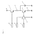
- Fig. 1 is a circuit diagram of a laser diode driving circuit in a first embodiment of the present invention.
- a laser diode 3 is of a plus driving type having a cathode connected to a ground.
- a first NPN transistor 1 is connected at a collector to a plus power source 30, at a base to a first power setting voltage input terminal 8, and at an emitter to an anode of the laser diode 3 through a first resistor 2.
- a second NPN transistor 4 is connected at a collector to the anode of the laser diode 3, at a base to an output terminal of a logic buffer 6, and at an emitter to the ground through a second resistor 5.
- the logic buffer 6 is connected at its input terminal to a data input terminal 7, and at its power supply terminal to a second power setting voltage input terminal 9.
- Fig. 2 is a signal waveform diagram showing an operation of the laser diode driving circuit in the first embodiment. Referring to Fig. 1 and Fig. 2, the operation of the first embodiment will be described below.
- a cutoff state (inactive state) of the second NPN transistor 4 when the voltage of the first power setting voltage input terminal 8 is raised to a first power setting voltage (first control voltage) as shown in a period "a" in Fig. 2, the first NPN transistor 1 becomes in an active state and supplies through the first resistor 2 to the laser diode 3 a current necessary for the laser diode 3 to produce a light output of a first power, so that the laser diode 3 emits a beam of light of the first power.
- the power of the light emitted from the laser diode 3 is switched between two values of power, that is, the first power and the second power.
- the voltage of the plus power source 30 may be +12 V
- the first power setting voltage may be a voltage selected in a range of 0 to +12 V
- the second power setting voltage may be +5 V
- the input data may be a modulated pulse voltage signal whose high level is +5 V and whose low level is 0 V.
- This embodiment in spite of a very simple constitution, provides a high speed performance at low cost because the NPN transistors and the logic buffer are used. Moreover, since the control voltages (first and second power setting voltages) for determining the power of the laser diode output light are based on the grounding point, or independent of the plus power source voltage, the power of the output light does not change even if the power source voltage fluctuates somewhat.
- Fig. 3 is a circuit diagram of a laser diode driving circuit in a second embodiment of the present invention.
- a two-bit logic buffer 10 having two parallel input terminals and two parallel output terminals is used.
- the input terminals of the two-bit logic buffer 10 are connected to a data A input terminal 11 for inputting a data A and a data B input terminal 12 for inputting a data B, respectively.
- the output terminals of the two-bit logic buffer 10 are for outputting buffered outputs of the data A and B, respectively, and are connected to the base of the second NPN transistor 4 through a third resistor 13 and a fourth resistor 14, respectively.
- the third and fourth resistors constitute a voltage combining circuit which combines the two buffered output voltages from the two-bit logic buffer 10 so that a combination of the two buffered voltages is applied to the base of the second NPN transistor 4.
- Fig. 4 is a signal waveform diagram showing an operation of the laser diode driving circuit of the second embodiment.
- the operation of the second embodiment will be described below with reference to Fig. 3 and Fig. 4. The explanation of the operation is also omitted in portions common to the first embodiment.
- the laser diode 3 is caused to emit a light of the first power as shown in a period "a" in Fig. 4.
- the data A input terminal 11 and the data B input terminal 12 are both set to a high voltage, and the supply voltage to the logic buffer 10 is raised to the second power setting voltage as shown in a period "b" in Fig. 4, so that the current of the laser diode 3 is decreased to emit a light of the second power.
- each of the data A at the data A input terminal 11 and the data B at the data B input terminal 12 are switched between a high level and a low level as shown in a period "c" in Fig. 4.
- the voltage combined by the voltage combining circuit constituted by the third resistor 13 and the fourth resistor 14 is highest, and the second NPN transistor 4 passes most of the current supplied from the first NPN transistor 1, so that the current of the laser diode 3 decreases most, and the light emitted from the laser diode 3 becomes the second power.
- both the data A and the data B are low level, to the contrary, the current of the laser diode 3 increases most to emit a light of the first power.
- the power of the emitted light becomes an intermediate value between the first power and the second power.
- the data A and the data B are input such that the switching timings thereof are shifted from each other as shown in period "c" in Fig. 4, the laser output can be modulated in four stages of power from the first power to the second power.
- the second embodiment may be modified such that data inputs are three or more bits, and the logic buffer is three-or-more-bit logic buffer to obtain a light output variable in more than four stages of power.
- Fig. 6 is a circuit diagram of a laser diode driving circuit in a third embodiment of the present invention.
- the base of the second NPN transistor 4 is connected to the input of the logic buffer 6 through a resistor 15, and to the ground through a resistor 16.
- the resistors 15 and 16 constitute a voltage dividing circuit for dividing the output voltage of the logic buffer 6.
- the voltage dividing circuit functions to adjust the base voltage of the second NPN transistor 4 so that the second NPN transistor 4 operates at an optimum operating point.
- the other parts of the third embodiment are exactly the same in constitution and operation as the first embodiment, and the signal waveform diagram is common to Fig. 2. Therefore, the light output of the laser diode 3 is switched between two values of power, that is, to be either the first power or the second power.
- Fig. 7 is a circuit diagram of a laser diode driving circuit in a fourth embodiment of the present invention.
- the elements identified with the same reference numerals as in the second embodiment function in the same way as in the second embodiment, explanation of them will be omitted.
- a third NPN transistor 21 is provided in addition to the first and second NPN transistors 1 and 4, a third NPN transistor 21 is provided.
- the third NPN transistor 21 is connected at a collector to the anode of the laser diode 3, and at an emitter to the ground through a resistor 22.
- the base of the second NPN transistor 4 is connected to one of the two outputs of the two-bit logic buffer 10 through a resistor 17, and to the ground through a resistor 18.
- the base of the third NPN transistor 21 is connected to the other of the two outputs of the two-bit logic buffer 10 through a resistor 19, and to the ground through a resistor 20.
- the resistors 17 and 18 constitute a voltage dividing circuit to divide the output voltage from one of the two outputs of the two-bit logic buffer 10, and the resistors 19 and 20 constitute another voltage dividing circuit to divide the output voltage from the other of the two outputs of the two-bit logic buffer 10.
- Fig. 8 is a signal waveform diagram showing an operation of the laser diode driving circuit of the fourth embodiment.
- the operation of the fourth embodiment will be described below with reference to Fig. 7 and Fig. 8. The explanation of the operation is omitted in portions common to the second embodiment.
- the laser diode 3 is caused to emit a light of the first power as shown in a period "a" in Fig. 8.
- the data A input terminal 11 is set high level and the data B input terminal 12 is set low level, and the supply voltage to the logic buffer 10 is raised to the second power setting voltage as shown in a period "b" in Fig. 8, so that the current of the laser diode 3 is decreased to emit a light of the second power.
- the data A and data B are switched in different switching patterns from each other as shown in a period "c" in Fig. 8.
- the current of the laser diode 3 becomes less than a threshold current necessary for the laser diode to emit light, so that the laser diode 3 stops emitting the light, that is, the light output power becomes zero power.
- the current of the laser diode 3 increases most to emit the light of the first power.
- the laser output can be modulated in three stages of the first power, the second power, and the zero power.
- the laser diode driving circuit of the present invention is effective to assure high speed in switching and stability against fluctuations of the power source voltage in spite of use of relatively inexpensive parts of NPN transistors as compared with PNP type transistors, although excellent in characteristics, and a simple structure using a general logic buffer. Therefore, when combined with an automatic laser power control circuit of feedback control, it is ideal as a laser driving circuit of optical disk device.
Landscapes
- Physics & Mathematics (AREA)
- Condensed Matter Physics & Semiconductors (AREA)
- General Physics & Mathematics (AREA)
- Electromagnetism (AREA)
- Optics & Photonics (AREA)
- Semiconductor Lasers (AREA)
- Optical Head (AREA)
Applications Claiming Priority (4)
| Application Number | Priority Date | Filing Date | Title |
|---|---|---|---|
| JP346791/95 | 1995-12-12 | ||
| JP34679195A JP3539524B2 (ja) | 1995-12-12 | 1995-12-12 | 半導体レーザ駆動回路 |
| JP34679195 | 1995-12-12 | ||
| US08/763,950 US5793786A (en) | 1995-12-12 | 1996-12-11 | Laser diode driving circuit |
Publications (2)
| Publication Number | Publication Date |
|---|---|
| EP0779688A1 true EP0779688A1 (fr) | 1997-06-18 |
| EP0779688B1 EP0779688B1 (fr) | 2001-03-14 |
Family
ID=26578356
Family Applications (1)
| Application Number | Title | Priority Date | Filing Date |
|---|---|---|---|
| EP96309032A Expired - Lifetime EP0779688B1 (fr) | 1995-12-12 | 1996-12-11 | Circuit d'alimentation pour un laser à diode |
Country Status (3)
| Country | Link |
|---|---|
| US (1) | US5793786A (fr) |
| EP (1) | EP0779688B1 (fr) |
| JP (1) | JP3539524B2 (fr) |
Cited By (1)
| Publication number | Priority date | Publication date | Assignee | Title |
|---|---|---|---|---|
| EP1544855A1 (fr) * | 2003-12-15 | 2005-06-22 | Thomson Licensing S.A. | Circuit compatible de modulation d'un laser pour un balayeur optique dans un appareil d'enregistrement/lecture d'un support optique |
Families Citing this family (17)
| Publication number | Priority date | Publication date | Assignee | Title |
|---|---|---|---|---|
| KR0185952B1 (ko) * | 1996-06-28 | 1999-04-15 | 김광호 | 레이저출력안정화서보 |
| JP2856247B2 (ja) * | 1996-11-12 | 1999-02-10 | 日本電気株式会社 | 消光比劣化を防止するapc方式 |
| JP2962263B2 (ja) * | 1997-02-13 | 1999-10-12 | 日本電気株式会社 | 半導体レーザ駆動回路 |
| JP3315892B2 (ja) * | 1997-04-24 | 2002-08-19 | 沖電気工業株式会社 | レーザーモジュールの制御回路 |
| US6002699A (en) * | 1998-02-27 | 1999-12-14 | Texas Instruments Incorporated | Semiconductor laser drive circuit |
| US6021143A (en) * | 1998-04-21 | 2000-02-01 | Lucent Technologies, Inc. | Dynamic control for laser diode drivers |
| US6021144A (en) * | 1999-02-24 | 2000-02-01 | Nvision, Inc. | Automatic power control circuit for a laser driver |
| US6930968B2 (en) | 2000-03-17 | 2005-08-16 | Matsushita Electric Industrial Co., Ltd. | Semiconductor laser driving apparatus with filter to attenuate enhanced frequency component and optical disk apparatus including the same |
| US6947458B2 (en) * | 2001-06-07 | 2005-09-20 | Alcatel Communications, Inc. | Power control circuit for laser diode having wavelength compensation |
| RU2222078C2 (ru) * | 2001-10-29 | 2004-01-20 | Общество с ограниченной ответственностью "Подсолнечник Технологии" | Устройство управления лазерным диодом (варианты) |
| TWM274702U (en) * | 2005-03-04 | 2005-09-01 | Sheng-He Chen | Voltage-dividing apparatus for prevention of power surge from laser diode |
| JP4803005B2 (ja) * | 2006-11-29 | 2011-10-26 | 住友電気工業株式会社 | 光受信器 |
| JP2011075919A (ja) * | 2009-09-30 | 2011-04-14 | Casio Computer Co Ltd | 光源装置、投影装置及び投影方法 |
| US20140226688A1 (en) * | 2013-02-11 | 2014-08-14 | Raytheon Company | Multiple output diode driver with independent current control and output current modulation |
| JP6367698B2 (ja) * | 2014-12-03 | 2018-08-01 | 日本電信電話株式会社 | ドライバ |
| JP2020088020A (ja) * | 2018-11-16 | 2020-06-04 | ソニーセミコンダクタソリューションズ株式会社 | 検出回路、駆動回路および発光装置 |
| EP3890125B1 (fr) * | 2018-11-27 | 2023-11-29 | Sony Semiconductor Solutions Corporation | Dispositif de commande et dispositif électroluminescent |
Citations (5)
| Publication number | Priority date | Publication date | Assignee | Title |
|---|---|---|---|---|
| JPS63285990A (ja) * | 1987-05-18 | 1988-11-22 | Nippon Telegr & Teleph Corp <Ntt> | レ−ザダイオ−ド駆動回路 |
| JPH02103984A (ja) * | 1988-10-13 | 1990-04-17 | Mitsubishi Electric Corp | 半導体レーザ駆動回路 |
| EP0495576A2 (fr) * | 1991-01-17 | 1992-07-22 | International Business Machines Corporation | Dispositif de commande d'un laser utilisé dans un entraînement de disque optique |
| JPH05315686A (ja) * | 1992-04-14 | 1993-11-26 | Sony Corp | レーザダイオード駆動回路 |
| EP0597644A1 (fr) * | 1992-11-12 | 1994-05-18 | Matsushita Electric Industrial Co., Ltd. | Circuit d'alimentation d'un laser à semi-conducteur |
Family Cites Families (2)
| Publication number | Priority date | Publication date | Assignee | Title |
|---|---|---|---|---|
| JPH0795610A (ja) * | 1993-09-21 | 1995-04-07 | Toshiba Corp | 色復調装置 |
| JPH07154015A (ja) * | 1993-12-01 | 1995-06-16 | Fujitsu Ltd | レーザダイオード駆動回路 |
-
1995
- 1995-12-12 JP JP34679195A patent/JP3539524B2/ja not_active Expired - Fee Related
-
1996
- 1996-12-11 US US08/763,950 patent/US5793786A/en not_active Expired - Fee Related
- 1996-12-11 EP EP96309032A patent/EP0779688B1/fr not_active Expired - Lifetime
Patent Citations (5)
| Publication number | Priority date | Publication date | Assignee | Title |
|---|---|---|---|---|
| JPS63285990A (ja) * | 1987-05-18 | 1988-11-22 | Nippon Telegr & Teleph Corp <Ntt> | レ−ザダイオ−ド駆動回路 |
| JPH02103984A (ja) * | 1988-10-13 | 1990-04-17 | Mitsubishi Electric Corp | 半導体レーザ駆動回路 |
| EP0495576A2 (fr) * | 1991-01-17 | 1992-07-22 | International Business Machines Corporation | Dispositif de commande d'un laser utilisé dans un entraînement de disque optique |
| JPH05315686A (ja) * | 1992-04-14 | 1993-11-26 | Sony Corp | レーザダイオード駆動回路 |
| EP0597644A1 (fr) * | 1992-11-12 | 1994-05-18 | Matsushita Electric Industrial Co., Ltd. | Circuit d'alimentation d'un laser à semi-conducteur |
Non-Patent Citations (3)
| Title |
|---|
| PATENT ABSTRACTS OF JAPAN vol. 013, no. 114 (E - 730) 20 March 1989 (1989-03-20) * |
| PATENT ABSTRACTS OF JAPAN vol. 014, no. 316 (E - 0949) 6 July 1990 (1990-07-06) * |
| PATENT ABSTRACTS OF JAPAN vol. 018, no. 120 (E - 1516) 25 February 1994 (1994-02-25) * |
Cited By (2)
| Publication number | Priority date | Publication date | Assignee | Title |
|---|---|---|---|---|
| EP1544855A1 (fr) * | 2003-12-15 | 2005-06-22 | Thomson Licensing S.A. | Circuit compatible de modulation d'un laser pour un balayeur optique dans un appareil d'enregistrement/lecture d'un support optique |
| WO2005059906A1 (fr) * | 2003-12-15 | 2005-06-30 | Thomson Licensing | Circuit de modulation de laser compatible pour scanner dans des appareils d'enregistrement/reproduction de supports a memoire optique |
Also Published As
| Publication number | Publication date |
|---|---|
| JP3539524B2 (ja) | 2004-07-07 |
| US5793786A (en) | 1998-08-11 |
| JPH09162473A (ja) | 1997-06-20 |
| EP0779688B1 (fr) | 2001-03-14 |
Similar Documents
| Publication | Publication Date | Title |
|---|---|---|
| US5793786A (en) | Laser diode driving circuit | |
| US5315606A (en) | Laser diode driving circuit | |
| EP0563580B1 (fr) | Circuit de commande pour dispositif émetteur de lumière | |
| US20010020670A1 (en) | Automatic power control circuit | |
| US4698527A (en) | TTL-ECL level converter operable with small time delay by controlling saturation | |
| EP0495576B1 (fr) | Dispositif de commande d'un laser utilisé dans un entraînement de disque optique | |
| EP0464813B1 (fr) | Circuit intégré pour activer une source de lumière et imprimante à laser utilisant un tel circuit | |
| JP3725235B2 (ja) | 発光素子駆動回路及びこれを有する発光装置 | |
| US5966110A (en) | Led driver | |
| US5059788A (en) | Optical logic device with PNPN detection and laser diode output | |
| US4868675A (en) | Control circuit for a laser printer | |
| US6717968B2 (en) | Laser drive device | |
| US5881081A (en) | Automatic laser power control circuit | |
| US7480463B2 (en) | LED drive circuit | |
| JPS60178735A (ja) | 発光素子駆動回路 | |
| KR20010080322A (ko) | 자기 주사형 발광 장치 | |
| US4900912A (en) | Driver circuit for semiconductor light-emitting device | |
| US6002699A (en) | Semiconductor laser drive circuit | |
| US20040156412A1 (en) | Driving device and light-emitting system for a laser diode | |
| DE69612067T2 (de) | Diodenlasertreiberschaltung | |
| JP3215166B2 (ja) | 光半導体素子の駆動回路 | |
| KR100262337B1 (ko) | 스위치드 저항을 사용한 전류제어 방식의 계조처리 전계방출표시소자 구동회로 | |
| JP2537290B2 (ja) | 半導体発光素子の駆動回路 | |
| JP4652495B2 (ja) | 半導体レーザ駆動回路 | |
| JPH02103984A (ja) | 半導体レーザ駆動回路 |
Legal Events
| Date | Code | Title | Description |
|---|---|---|---|
| PUAI | Public reference made under article 153(3) epc to a published international application that has entered the european phase |
Free format text: ORIGINAL CODE: 0009012 |
|
| AK | Designated contracting states |
Kind code of ref document: A1 Designated state(s): DE FR GB |
|
| 17P | Request for examination filed |
Effective date: 19971111 |
|
| 17Q | First examination report despatched |
Effective date: 19990406 |
|
| GRAG | Despatch of communication of intention to grant |
Free format text: ORIGINAL CODE: EPIDOS AGRA |
|
| 17Q | First examination report despatched |
Effective date: 19990406 |
|
| GRAG | Despatch of communication of intention to grant |
Free format text: ORIGINAL CODE: EPIDOS AGRA |
|
| GRAH | Despatch of communication of intention to grant a patent |
Free format text: ORIGINAL CODE: EPIDOS IGRA |
|
| GRAH | Despatch of communication of intention to grant a patent |
Free format text: ORIGINAL CODE: EPIDOS IGRA |
|
| GRAH | Despatch of communication of intention to grant a patent |
Free format text: ORIGINAL CODE: EPIDOS IGRA |
|
| GRAA | (expected) grant |
Free format text: ORIGINAL CODE: 0009210 |
|
| AK | Designated contracting states |
Kind code of ref document: B1 Designated state(s): DE FR GB |
|
| RIC1 | Information provided on ipc code assigned before grant |
Free format text: 7H 01S 5/042 A |
|
| REF | Corresponds to: |
Ref document number: 69612067 Country of ref document: DE Date of ref document: 20010419 |
|
| ET | Fr: translation filed | ||
| REG | Reference to a national code |
Ref country code: GB Ref legal event code: IF02 |
|
| PLBE | No opposition filed within time limit |
Free format text: ORIGINAL CODE: 0009261 |
|
| STAA | Information on the status of an ep patent application or granted ep patent |
Free format text: STATUS: NO OPPOSITION FILED WITHIN TIME LIMIT |
|
| 26N | No opposition filed | ||
| PGFP | Annual fee paid to national office [announced via postgrant information from national office to epo] |
Ref country code: GB Payment date: 20051207 Year of fee payment: 10 |
|
| PGFP | Annual fee paid to national office [announced via postgrant information from national office to epo] |
Ref country code: FR Payment date: 20051208 Year of fee payment: 10 |
|
| PGFP | Annual fee paid to national office [announced via postgrant information from national office to epo] |
Ref country code: DE Payment date: 20051209 Year of fee payment: 10 |
|
| PG25 | Lapsed in a contracting state [announced via postgrant information from national office to epo] |
Ref country code: DE Free format text: LAPSE BECAUSE OF NON-PAYMENT OF DUE FEES Effective date: 20070703 |
|
| GBPC | Gb: european patent ceased through non-payment of renewal fee |
Effective date: 20061211 |
|
| REG | Reference to a national code |
Ref country code: FR Ref legal event code: ST Effective date: 20070831 |
|
| PG25 | Lapsed in a contracting state [announced via postgrant information from national office to epo] |
Ref country code: GB Free format text: LAPSE BECAUSE OF NON-PAYMENT OF DUE FEES Effective date: 20061211 |
|
| PG25 | Lapsed in a contracting state [announced via postgrant information from national office to epo] |
Ref country code: FR Free format text: LAPSE BECAUSE OF NON-PAYMENT OF DUE FEES Effective date: 20070102 |