EP0779715A2 - Tastaturstruktur zur Reduktion von elektromagnetischen Einflüssen - Google Patents
Tastaturstruktur zur Reduktion von elektromagnetischen Einflüssen Download PDFInfo
- Publication number
- EP0779715A2 EP0779715A2 EP96119396A EP96119396A EP0779715A2 EP 0779715 A2 EP0779715 A2 EP 0779715A2 EP 96119396 A EP96119396 A EP 96119396A EP 96119396 A EP96119396 A EP 96119396A EP 0779715 A2 EP0779715 A2 EP 0779715A2
- Authority
- EP
- European Patent Office
- Prior art keywords
- keyboard
- row
- keyboard structure
- column
- coupled
- Prior art date
- Legal status (The legal status is an assumption and is not a legal conclusion. Google has not performed a legal analysis and makes no representation as to the accuracy of the status listed.)
- Withdrawn
Links
- 239000004020 conductor Substances 0.000 claims abstract description 52
- 230000008878 coupling Effects 0.000 claims description 34
- 238000010168 coupling process Methods 0.000 claims description 34
- 238000005859 coupling reaction Methods 0.000 claims description 34
- 230000000994 depressogenic effect Effects 0.000 claims description 3
- 230000004913 activation Effects 0.000 claims 1
- 229910052751 metal Inorganic materials 0.000 abstract description 9
- 239000002184 metal Substances 0.000 abstract description 9
- 239000004065 semiconductor Substances 0.000 description 7
- 230000005670 electromagnetic radiation Effects 0.000 description 5
- 238000009413 insulation Methods 0.000 description 5
- 230000001012 protector Effects 0.000 description 5
- 230000005855 radiation Effects 0.000 description 3
- 230000003068 static effect Effects 0.000 description 3
- 238000003491 array Methods 0.000 description 2
- 230000005611 electricity Effects 0.000 description 2
- 239000011888 foil Substances 0.000 description 2
- 230000033228 biological regulation Effects 0.000 description 1
- 230000015572 biosynthetic process Effects 0.000 description 1
- 230000015556 catabolic process Effects 0.000 description 1
- 230000008859 change Effects 0.000 description 1
- 238000006243 chemical reaction Methods 0.000 description 1
- 239000000428 dust Substances 0.000 description 1
- 230000002452 interceptive effect Effects 0.000 description 1
- 239000000463 material Substances 0.000 description 1
- 238000005259 measurement Methods 0.000 description 1
- 230000007246 mechanism Effects 0.000 description 1
- 230000010287 polarization Effects 0.000 description 1
- 229910052709 silver Inorganic materials 0.000 description 1
- 239000004332 silver Substances 0.000 description 1
- 230000007480 spreading Effects 0.000 description 1
- XLYOFNOQVPJJNP-UHFFFAOYSA-N water Substances O XLYOFNOQVPJJNP-UHFFFAOYSA-N 0.000 description 1
Images
Classifications
-
- H—ELECTRICITY
- H03—ELECTRONIC CIRCUITRY
- H03M—CODING; DECODING; CODE CONVERSION IN GENERAL
- H03M11/00—Coding in connection with keyboards or like devices, i.e. coding of the position of operated keys
- H03M11/22—Static coding
- H03M11/24—Static coding using analogue means, e.g. by coding the states of multiple switches into a single multi-level analogue signal or by indicating the type of a device using the voltage level at a specific tap of a resistive divider
-
- H—ELECTRICITY
- H01—ELECTRIC ELEMENTS
- H01H—ELECTRIC SWITCHES; RELAYS; SELECTORS; EMERGENCY PROTECTIVE DEVICES
- H01H13/00—Switches having rectilinearly-movable operating part or parts adapted for pushing or pulling in one direction only, e.g. push-button switch
- H01H13/70—Switches having rectilinearly-movable operating part or parts adapted for pushing or pulling in one direction only, e.g. push-button switch having a plurality of operating members associated with different sets of contacts, e.g. keyboard
- H01H13/702—Switches having rectilinearly-movable operating part or parts adapted for pushing or pulling in one direction only, e.g. push-button switch having a plurality of operating members associated with different sets of contacts, e.g. keyboard with contacts carried by or formed from layers in a multilayer structure, e.g. membrane switches
-
- H—ELECTRICITY
- H01—ELECTRIC ELEMENTS
- H01H—ELECTRIC SWITCHES; RELAYS; SELECTORS; EMERGENCY PROTECTIVE DEVICES
- H01H2239/00—Miscellaneous
- H01H2239/004—High frequency adaptation or shielding
-
- H—ELECTRICITY
- H01—ELECTRIC ELEMENTS
- H01H—ELECTRIC SWITCHES; RELAYS; SELECTORS; EMERGENCY PROTECTIVE DEVICES
- H01H2239/00—Miscellaneous
- H01H2239/008—Static electricity considerations
-
- H—ELECTRICITY
- H01—ELECTRIC ELEMENTS
- H01H—ELECTRIC SWITCHES; RELAYS; SELECTORS; EMERGENCY PROTECTIVE DEVICES
- H01H2239/00—Miscellaneous
- H01H2239/01—Miscellaneous combined with other elements on the same substrate
- H01H2239/012—Decoding impedances
-
- H—ELECTRICITY
- H01—ELECTRIC ELEMENTS
- H01H—ELECTRIC SWITCHES; RELAYS; SELECTORS; EMERGENCY PROTECTIVE DEVICES
- H01H2239/00—Miscellaneous
- H01H2239/018—Ground conductor
Definitions
- the present invention relates generally to reducing electromagnetic interference in keyboard devices, and particularly to a film keyboard structure which reduces electromagnetic interference.
- Electromagnetic interference here refers particularly to ESD, Electro Static Discharge, and to RFI, Radio Frequency Interference.
- electrostatic charges When objects and people move in relation to each other, there are created electrostatic charges, where the potential differences may be several thousands of volts, but the amount of energy bound in these charges is usually insignificant.
- the charges are discharged suddenly, when two charged objects fall so near to each other that the breakdown insulation in the materials in between is not sufficient, or when the electricity otherwise finds a path with a sufficiently low resistance.
- the charge may be discharged in one or several pulses. These discharges are not dangerous for people, but electronic appliances contain a lot of semiconductor components that are sensitive to static electricity. If an electrostatic charge is discharged through a semiconductor component, its inner structure may be damaged, even if the potential difference were only a few hundreds of volts.
- moving electric charges cause electromagnetic radiation.
- Particularly high-frequency electric signals which are meant to proceed in conductors, create an electromagnetic radiation field in the surroundings.
- the radiation and the movement of the electric charges are interactive, so that the said electromagnetic radiation field may in part cause undesired phenomena in other electronic devices.
- International and national standards and regulations set given limit values, which represent the maximum of the radiation emitted from electric appliances at different frequencies. Measurements are generally carried out in a frequency range of 30 - 1,000 MHz and with varying polarization.
- Electro Magnetic Compatibility is a general concept which, when applied to electronic devices, includes for instance the tolerance of electrostatic discharges and the fact that the device does not emit radiation above a given level nor is itself disturbed by external electromagnetic radiation. Devices must be planned and built so that they fulfill the respective EMC requirements.
- a film keyboard comprises several planar layers arranged on top of each other; the said layers may contain separate parts for individual keys, but the film keyboard forms an essentially uniform external surface as a difference from keyboards constructed of several different press keys, where the keys are independently moving tiny mechanisms.
- Film keyboards can be extremely easily integrated to form a part of the casing of an electronic device, and they are useful particularly in applications where the device plus keyboard must be inside a compact casing in order to achieve water or dust resistance, for instance.
- the keys are divided into rows and columns, which are named so that in the normal operation position, the rows are essentially horizontal and the columns essentially vertical.
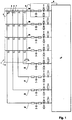
- the keys in a film keyboard do not have to be in any regular order, but it is simplest to describe the features of the prior art by observing a regular square keyboard illustrated in figure 1. It comprises 16 keys 2, as well as row wires 3a, 3b, 3c, 3d and column wires 4a, 4b, 4c, 4d, which are insulated from each other.
- the keys 2 are located essentially at the junctions of the row and column conductors, so that each key contains contact surfaces 5 and 6 in connection to the intersecting row and column conductor, as well as a metal spring or bubble 7. When a key is pressed, the metal spring or bubble 7 is pushed against the contact surfaces 5 and 6 and thus forms a low-resistance connection therebetween.
- the topmost layer of the keyboard is an insulation layer, which for the sake of clarity is not illustrated in figure 1. Underneath it, there are the metal springs or bubbles 7 and the row and column wires with their contact surfaces. In between different conductor parts, there are provided insulation layers. The thickness and mutual arrangement of the conductor and insulation layers may vary depending on the desired properties of the keyboard in question.
- a microprocessor 8 or a similar apparatus reads the keyboard 1 for instance so that it normally keeps all rows 3a, 3b, 3c, 3d on a level corresponding to the TTL signal "1", but regularly writes for each row a momentary level "0".
- the columns 4a, 4b, 4c, 4d are normally switched with so-called pull-up resistors to level "1", but if a given key is pressed at the same time as the corresponding row has the value "0", the key switches the said column to level "0", which is detected in the processor 8.
- the processor interprets a simultaneous level "0" of a given row and column as a depression of the key located at their junction.
- TTL signal levels means that in order to make this kind of keyboard to work, the elements taking part in the key switching operation must not at any stage be coupled to ground potential.
- a traditional film keyboard is generally coupled directly to a microprocessor 8 or to one of its auxiliary circuits (such as a bus buffer, not illustrated in the drawing), which is essentially a semiconductor circuit and thus normally sensitive to electrostatic discharges. If the device does not have ESD protection, the static charge of the user touching the keyboard may be discharged through the topmost insulation layer of the keyboard to the metal spring or bubble 7 and thereby to the microprocessor 8 along the row and/or column conductors 3a - 3d, 4a - 4d. As was in general terms explained above, the discharge may damage the inner structure of the microprocessor. Moreover, a rapid reading cycle, i.e. changing the TTL levels in the row conductors 3a - 3d, as well as other rapid mode changes of the microprocessor 8, which changes are coupled to the keyboard conductors, may cause electromagnetic radiation through the keyboard.
- a rapid reading cycle i.e. changing the TTL levels in the row conductors 3a - 3d, as well as other rapid mode changes of the micro
- the first alternative is to use protector components 9, which comprise serial resistors and clamp diodes.
- each signal line connected to the processor 8 must be provided with its own protector components.
- the protection of one row requires six components, and even a small 4 x 4 keyboard contains eight rows, which means that the total number of protector components rises up to 48. These take up space around the processor, cause losses and increase production expenses.
- ground plane 10 covering the whole keyboard, which ground plane is called ESD ground or RFI ground and is the first conducting layer when starting from the keyboard surface.
- ESD ground or RFI ground is the first conducting layer when starting from the keyboard surface.
- RFI ground is the ground plane 10 covering the whole keyboard
- the purpose is that the electrostatic discharge emitted from the user is conducted to the ground potential through the ground plane 10, and is thus not conducted to other structures of the keyboard, wherefore the ground plane 10 must be completely insulated from the metal springs or bubbles 7 and conductors 3a - 4d. If the spreading of radio frequency interference RFI to the surroundings should also be prevented, the ground plane 10 must be essentially uniform.
- the production of a separate plane to the layer structure of the film keyboard and the use of metal (generally silver) in the formation of a uniform ground plane both increase production costs.
- the object of the present invention is to introduce a keyboard structure which enables the realization of EMC protection in an advantageous fashion and is applicable to film keyboards.
- Another object of the invention is to introduce a keyboard structure which requires only a limited amount of separate protector components against electromagnetic interference.
- Yet another object of the invention is that the invented structure is well suited to the serial production of keyboards and that the ensuing production costs are reasonable.
- the objects of the invention are achieved by coupling the switching member, which causes the switching operation corresponding to a depression of a key, to ground potential ad by arranging the reading of the keyboard so that its conductors can be coupled to ground potential in connection with a keystroke.
- the keyboard structure according to the invention comprising a switching member for each press key, is characterized in that the said switching member is permanently coupled to ground potential.
- the invention is based on the realization that the switching member itself, the one that causes the switching operation corresponding to a keystroke, can be permanently coupled to ground potential, in which case an electrostatic discharge directed thereto is immediately coupled to ground and does not create interference pulses extending as far as the semiconductor components. Now the reading of the keyboard must naturally be realized so that its conductors can, in connection with a keystroke, be coupled to ground potential.
- there are formed resistance networks for the row and column parts of the keyboard so that a given row and a given column always correspond to a given point in the connected resistor network.
- a RFI protection by using protector components in connection with the signal lines connected to the processor. Because a preferred embodiment of the invention advantageously contains only two signal lines and the keyboard operates on direct-current voltage, the number of required components is low and the components can be dimensioned so that they cause as little losses as possible.
- the conductors corresponding to the rows and columns of the keyboard are maintained at a given potential other than zero when no key is being pressed.
- its grounded switching member In connection with the depression of a given key, its grounded switching member connects one row conductor and one column conductor to ground. A change in the potential of the conductors is interpreted as a keystroke.
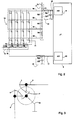
- Figure 2 illustrates a preferred embodiment of the keyboard structure according to the present invention, as well as its coupling to a microprocessor 8.
- the microprocessor 8 is an exemplary device and represents any circuit arrangement containing semiconductor components, which circuit is controlled by means of a keyboard, and where it is necessary to pay attention to the electromagnetic protection of the arrangement.
- the keyboard structure of figure 2 comprises two resistor networks, i.e. arrays 11 and 12 of resistors coupled in series, both arrays being at one end coupled to the supply voltage marked Vcc.
- the first resistor network 11 corresponds to the rows of the keyboard 13 and comprises the serially coupled resistors R1, R2, R3 and R4, of which the first end of the resistor R1 is coupled to the supply voltage.
- the second resistor network 12 corresponds to the columns of the keyboard 13 and comprises the serially coupled resistors R5, R6, R7 and R8, of which the first end of the resistor R5 is coupled to the supply voltage Vcc.
- the coupling junction 14 between the resistors R1 and R2 is coupled both to the keyboard conductor 3a leading to the keys of the first row and to the row input 15 of the microprocessor.
- the coupling junction between the resistors R2 and R3 is coupled to the keyboard conductor 3b leading to the keys of the second row
- the coupling junction between the resistors R3 and R4 is coupled to the keyboard conductor 3c leading to the keys of the third row
- the end of the resistor R4 is coupled to the keyboard conductor 3d leading to the keys of the fourth row.
- the coupling junction 16 between the resistors R5 and R6 is coupled both to the keyboard conductor 4a leading to the keys of the first column and to the column input 17 of the microprocessor.
- the coupling junction between the resistors R6 and R7 is coupled to the keyboard conductor 4b leading to the keys of the second column
- the coupling junction between the resistors R7 and R8 is coupled to the keyboard conductor 4c leading to the keys of the third column
- the end of the resistor R8 is coupled to the keyboard conductor 4d leading to the keys of the fourth column.
- the coupling junctions 14 and 16 are coupled to the row input 15 and column input 17 of the microprocessor 8 via filter couplings 21 and 22. The purpose of these will be discussed later on.
- each key comprises contact surfaces 5 and 6 connected to the row and column conductors 3, 4 which intersect at the key in question, as well as a switching member 7 which can as such be a similar metal spring or bubble as in the keyboard structures of the prior art, except that it is coupled to ground potential for instance by means of a strip-like conductor or foil conductor 18, which in the case of a film keyboard lies in a given layer of the film structure and connects all switching members.
- the switching member 7 provided in the key forms a low-resistance connection in between the contact surfaces 5 and 6 of the key, which then couples the end of the last resistor of each resistor network 11 and 12 (in the row resistor network 11 resistor R4 and in the column resistor network 12 resistor R8) to ground potential.
- the depression of any of the keys in the lowest row causes in the coupling junction 14 the same potential as in the formula (1), and the depression of any of the keys in the left-hand side column causes in the coupling junction 16 the same potential as in the formula (2).
- the potential conforms to each row and column on a more general level, too.
- the microprocessor 8 obtains as signal inputs a digital value pair which unambiguously corresponds to the depression of a given key. This value pair can be further processed in the microprocessor in ways known in the prior art.
- the resolution of the A/D converters 19 and 20 determines how many different voltage values can be identified at the coupling junctions 14 and 16, i.e. how many rows and columns the keyboard can have.
- a depression of any of the keys in the highest row connects the coupling junction 14 essentially to ground potential, and the depression of any of the keys in the lowest row connects the coupling junction 14 to the potential according to the formula (1).
- the values of the resistors in the resistor network 11 must be chosen so that the potential values corresponding to other rows fall in between these extreme values with intervals that are at least the size of the resolution capacity of the A/D converter 19.
- the filter couplings 21 and 22 realize the RFI protection. Because the keyboard 13 works only with slowly changing direct-current voltages, it does not create radio frequency interference itself. Rapid inner mode changes of the microprocessor 8 may cause high-frequency signal components which tend to be coupled to the conductors leading out of the processor. The proceeding of interferences as far as the keyboard is prevented by forming in front of both the row and column inputs a filter circuit 21, 22 according to a prior art low pass structure, which filter circuit comprises a fairly large serial resistor R21, R22 and a fairly small capacitance C21, C22, which is coupled in between one end of the said serial resistor and ground potential.
- serial resistors R21 and R22 can be large, because the potential values of the coupling junctions 14 and 16 corresponding to the keystrokes do not require much current in order to be transmitted; remarkable power losses are therefore not caused in the serial resistors.
- Other types of filter couplings known as such for those skilled in the art, can be used for attenuating high-frequency interference in the conductors in between the microprocessor 8 and the keyboard 13.
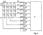
- FIG 4 shows another preferred embodiment of the invention, where voltage division couplings are not applied for each row and column individually, but every row conductor 3a - 3d and every column conductor 4a - 4d forms its own supply line to the microprocessor 8, in the same fashion as in the prior art arrangement illustrated in figure 1.
- the principal idea is that the processor 8 maintains all row and column conductors 3a - 4d all the time in a given potential other than zero, for example by means of so-called pull-up resistors (not illustrated in the drawing).
- Each press key comprises a switching member 7, which again is a similar metal spring or bubble as in the embodiments illustrated in figures 1 - 3.
- the switching members 7 of all keys are coupled to ground by the foil conductor 18.
- the preferred embodiments of the invention are described with reference to two-dimensional keyboards, where the keys are grouped in rows and columns, and where each row and column is provided with a corresponding conductor running along the whole length of the respective row or column.
- the invention is easily applied to keyboards where the grouping of the keys differs from the one described above, or where several auxiliary conductors are used for each row and/or column.
- the keyboard according to the invention may also contain only one key, one row or one column.
- the present invention brings forth remarkable advantages as compared to the prior art, because the number of auxiliary components required for the EMC protection in the immediate vicinity of the semiconductor component coupled to the keyboard is considerably reduced. This saves both board space and production expenses.
- the keyboard When the keyboard is operated with direct-current voltages, which shift their mode slowly, it can itself serve as the ESD protection.
- a uniform RFI protection layer is not needed, but the protection against radio frequency interference can be arranged by means of a few filter couplings.
- Admittedly a preferred embodiment of the invention presupposes that the keyboard signals are A/D-converted in the processor or in the immediate vicinity thereof, but because many commercially available microprocessors already include suitable A/D converters, this is not an immoderate requirement.
Landscapes
- Engineering & Computer Science (AREA)
- Theoretical Computer Science (AREA)
- Push-Button Switches (AREA)
- Input From Keyboards Or The Like (AREA)
Applications Claiming Priority (2)
| Application Number | Priority Date | Filing Date | Title |
|---|---|---|---|
| FI956005 | 1995-12-14 | ||
| FI956005A FI100142B (fi) | 1995-12-14 | 1995-12-14 | Sähkömagneettisia häiriöitä vähentävä näppäimistörakenne |
Publications (2)
| Publication Number | Publication Date |
|---|---|
| EP0779715A2 true EP0779715A2 (de) | 1997-06-18 |
| EP0779715A3 EP0779715A3 (de) | 1998-09-30 |
Family
ID=8544545
Family Applications (1)
| Application Number | Title | Priority Date | Filing Date |
|---|---|---|---|
| EP96119396A Withdrawn EP0779715A3 (de) | 1995-12-14 | 1996-12-04 | Tastaturstruktur zur Reduktion von elektromagnetischen Einflüssen |
Country Status (2)
| Country | Link |
|---|---|
| EP (1) | EP0779715A3 (de) |
| FI (1) | FI100142B (de) |
Cited By (6)
| Publication number | Priority date | Publication date | Assignee | Title |
|---|---|---|---|---|
| WO2001031567A1 (en) * | 1999-10-22 | 2001-05-03 | Ericsson Inc | Handwritten character recognition devices and electronic devices incorporating same |
| WO2002091589A1 (en) * | 2001-05-09 | 2002-11-14 | Comex Electronics Ab | Method and device for signal protection |
| WO2006024131A1 (en) | 2004-08-31 | 2006-03-09 | Research In Motion Limited | Mobile wireless communications device with reduced interference from the keyboard into the radio receiver |
| EP1790185A4 (de) * | 2004-08-31 | 2007-12-05 | Research In Motion Ltd | Mobiles drahtloses kommunikationsgerät mit verringerter störenergie von der tastatur |
| FR2910652A1 (fr) * | 2006-12-21 | 2008-06-27 | Dav Sa | Module de commande electrique, en particulier pour vehicule automobile |
| US7425904B2 (en) | 2004-11-23 | 2008-09-16 | Qisda Corporation | Keypad circuit with electrostatic discharge protection |
Families Citing this family (1)
| Publication number | Priority date | Publication date | Assignee | Title |
|---|---|---|---|---|
| CN114035697B (zh) * | 2021-11-26 | 2023-10-03 | 中国电子技术标准化研究院 | 一种低辐射抗电磁干扰的键盘鼠标模拟装置及方法 |
Family Cites Families (3)
| Publication number | Priority date | Publication date | Assignee | Title |
|---|---|---|---|---|
| FR2370348A1 (fr) * | 1976-11-05 | 1978-06-02 | Leveille Marc | Contacteur matriciel pour affichage video notamment |
| GB2102626B (en) * | 1981-07-21 | 1985-06-05 | Standard Telephones Cables Ltd | Contact dimple pad |
| US4725816A (en) * | 1984-12-10 | 1988-02-16 | John Fluke Mfg. Co., Inc. | Matrix keyboard encoder circuit |
-
1995
- 1995-12-14 FI FI956005A patent/FI100142B/fi active
-
1996
- 1996-12-04 EP EP96119396A patent/EP0779715A3/de not_active Withdrawn
Non-Patent Citations (1)
| Title |
|---|
| None |
Cited By (12)
| Publication number | Priority date | Publication date | Assignee | Title |
|---|---|---|---|---|
| WO2001031567A1 (en) * | 1999-10-22 | 2001-05-03 | Ericsson Inc | Handwritten character recognition devices and electronic devices incorporating same |
| US6477274B1 (en) | 1999-10-22 | 2002-11-05 | Ericsson Inc. | Handwritten character recognition devices and electronic devices incorporating same |
| WO2002091589A1 (en) * | 2001-05-09 | 2002-11-14 | Comex Electronics Ab | Method and device for signal protection |
| US7356626B2 (en) * | 2001-05-09 | 2008-04-08 | Comex Electronics Ab | Method and device for signal protection |
| WO2006024131A1 (en) | 2004-08-31 | 2006-03-09 | Research In Motion Limited | Mobile wireless communications device with reduced interference from the keyboard into the radio receiver |
| EP1795024A4 (de) * | 2004-08-31 | 2007-10-31 | Research In Motion Ltd | Mobiles drahtloses kommunikationsgerät mit verringerten störungen von der tastatur in den funkempfänger |
| EP1790185A4 (de) * | 2004-08-31 | 2007-12-05 | Research In Motion Ltd | Mobiles drahtloses kommunikationsgerät mit verringerter störenergie von der tastatur |
| US7363063B2 (en) | 2004-08-31 | 2008-04-22 | Research In Motion Limited | Mobile wireless communications device with reduced interference from the keyboard into the radio receiver |
| US7387256B2 (en) | 2004-08-31 | 2008-06-17 | Research In Motion Limited | Mobile wireless communications device with reduced interfering energy from the keyboard |
| US7425904B2 (en) | 2004-11-23 | 2008-09-16 | Qisda Corporation | Keypad circuit with electrostatic discharge protection |
| FR2910652A1 (fr) * | 2006-12-21 | 2008-06-27 | Dav Sa | Module de commande electrique, en particulier pour vehicule automobile |
| WO2008080812A1 (fr) * | 2006-12-21 | 2008-07-10 | Dav | Module de commande electrique, en particulier pour vehicule automobile |
Also Published As
| Publication number | Publication date |
|---|---|
| FI956005L (fi) | 1997-06-15 |
| EP0779715A3 (de) | 1998-09-30 |
| FI956005A0 (fi) | 1995-12-14 |
| FI100142B (fi) | 1997-09-30 |
Similar Documents
| Publication | Publication Date | Title |
|---|---|---|
| US4561002A (en) | Capacitive touch switch arrangement | |
| US7075523B2 (en) | Data acquisition from capacitive touch pad | |
| DE102009017419B4 (de) | Kapazitiver Positionssensor | |
| CN102200866B (zh) | 互电容触摸感应装置及其检测方法、触摸显示装置 | |
| US8711113B2 (en) | Modular connector for touch sensitive device | |
| CN107315504B (zh) | 一种阵列基板、显示面板及显示装置 | |
| US5668384A (en) | Input protection device with Zener diodes for electronic device | |
| KR101505041B1 (ko) | 재구성가능한 검출점을 갖는 터치패널 및 그 검출 방법 | |
| WO2005043595A2 (en) | Electric field proximity keyboards and detection systems | |
| KR20100081963A (ko) | 터치 패널의 신호 처리 장치 및 입력 장치 | |
| CN104238846A (zh) | 触控装置及感测补偿方法 | |
| EP0779715A2 (de) | Tastaturstruktur zur Reduktion von elektromagnetischen Einflüssen | |
| US3755686A (en) | Powerplexer | |
| KR20150031767A (ko) | 터치패널 | |
| CN109164935B (zh) | 触控显示面板、触控驱动电路和触控驱动方法 | |
| CN104007871A (zh) | 触摸板输入装置及其触摸板输入检测方法 | |
| CN102736773A (zh) | 未接地的触控输入装置及其控制装置 | |
| CN103970376A (zh) | 电容式触控装置及其触控感测方法 | |
| US7675723B2 (en) | Transient to digital converters | |
| US20030200652A1 (en) | Method for improving EMC of keyboard soft board | |
| US5034740A (en) | Capacitive card module | |
| CN101989138A (zh) | 触控面板装置、感测控制装置以及触控面板的控制方法 | |
| CN113778265B (zh) | 触控面板、显示装置和控制方法 | |
| CN213122936U (zh) | 触控显示面板及电子设备 | |
| KR20240111976A (ko) | 정전용량 측정기능 및 유도전압 측정기능을 동시에 구현하는 전극구조를 포함하는 장치 |
Legal Events
| Date | Code | Title | Description |
|---|---|---|---|
| PUAI | Public reference made under article 153(3) epc to a published international application that has entered the european phase |
Free format text: ORIGINAL CODE: 0009012 |
|
| AK | Designated contracting states |
Kind code of ref document: A2 Designated state(s): DE FR GB IT |
|
| PUAL | Search report despatched |
Free format text: ORIGINAL CODE: 0009013 |
|
| AK | Designated contracting states |
Kind code of ref document: A3 Designated state(s): DE FR GB IT |
|
| STAA | Information on the status of an ep patent application or granted ep patent |
Free format text: STATUS: THE APPLICATION IS DEEMED TO BE WITHDRAWN |
|
| 18D | Application deemed to be withdrawn |
Effective date: 19990701 |