EP0780717B1 - Isolateur optique et élément optique avec un revêtement résistant à la chaleur et anti-réfléchissant - Google Patents
Isolateur optique et élément optique avec un revêtement résistant à la chaleur et anti-réfléchissant Download PDFInfo
- Publication number
- EP0780717B1 EP0780717B1 EP96309199A EP96309199A EP0780717B1 EP 0780717 B1 EP0780717 B1 EP 0780717B1 EP 96309199 A EP96309199 A EP 96309199A EP 96309199 A EP96309199 A EP 96309199A EP 0780717 B1 EP0780717 B1 EP 0780717B1
- Authority
- EP
- European Patent Office
- Prior art keywords
- optical isolator
- analyser
- polariser
- alloy
- optical
- Prior art date
- Legal status (The legal status is an assumption and is not a legal conclusion. Google has not performed a legal analysis and makes no representation as to the accuracy of the status listed.)
- Expired - Lifetime
Links
- 230000003287 optical effect Effects 0.000 title claims description 75
- 239000011248 coating agent Substances 0.000 title 1
- 238000000576 coating method Methods 0.000 title 1
- 229910045601 alloy Inorganic materials 0.000 claims description 33
- 239000000956 alloy Substances 0.000 claims description 33
- 239000011521 glass Substances 0.000 claims description 18
- 229910000679 solder Inorganic materials 0.000 claims description 14
- 238000005476 soldering Methods 0.000 claims description 10
- 229910000833 kovar Inorganic materials 0.000 claims description 9
- BASFCYQUMIYNBI-UHFFFAOYSA-N platinum Chemical compound [Pt] BASFCYQUMIYNBI-UHFFFAOYSA-N 0.000 claims description 6
- 229910001030 Iron–nickel alloy Inorganic materials 0.000 claims description 5
- JVPLOXQKFGYFMN-UHFFFAOYSA-N gold tin Chemical compound [Sn].[Au] JVPLOXQKFGYFMN-UHFFFAOYSA-N 0.000 claims description 5
- BYDQGSVXQDOSJJ-UHFFFAOYSA-N [Ge].[Au] Chemical compound [Ge].[Au] BYDQGSVXQDOSJJ-UHFFFAOYSA-N 0.000 claims description 4
- PCHJSUWPFVWCPO-UHFFFAOYSA-N gold Chemical compound [Au] PCHJSUWPFVWCPO-UHFFFAOYSA-N 0.000 claims description 4
- 229910052737 gold Inorganic materials 0.000 claims description 4
- 239000010931 gold Substances 0.000 claims description 4
- VYZAMTAEIAYCRO-UHFFFAOYSA-N Chromium Chemical compound [Cr] VYZAMTAEIAYCRO-UHFFFAOYSA-N 0.000 claims description 3
- 229910000927 Ge alloy Inorganic materials 0.000 claims description 3
- 229910001128 Sn alloy Inorganic materials 0.000 claims description 3
- 229910052804 chromium Inorganic materials 0.000 claims description 3
- 239000011651 chromium Substances 0.000 claims description 3
- 229910052697 platinum Inorganic materials 0.000 claims description 3
- 238000010791 quenching Methods 0.000 description 48
- 230000000171 quenching effect Effects 0.000 description 48
- 238000000034 method Methods 0.000 description 17
- 238000009863 impact test Methods 0.000 description 14
- 238000001465 metallisation Methods 0.000 description 14
- 238000002474 experimental method Methods 0.000 description 9
- 238000005259 measurement Methods 0.000 description 9
- 230000000052 comparative effect Effects 0.000 description 8
- 239000010410 layer Substances 0.000 description 8
- 230000015572 biosynthetic process Effects 0.000 description 7
- XEEYBQQBJWHFJM-UHFFFAOYSA-N Iron Chemical compound [Fe] XEEYBQQBJWHFJM-UHFFFAOYSA-N 0.000 description 6
- PXHVJJICTQNCMI-UHFFFAOYSA-N Nickel Chemical compound [Ni] PXHVJJICTQNCMI-UHFFFAOYSA-N 0.000 description 6
- 239000000463 material Substances 0.000 description 6
- 230000003247 decreasing effect Effects 0.000 description 5
- 238000009826 distribution Methods 0.000 description 5
- 238000012360 testing method Methods 0.000 description 5
- 230000008646 thermal stress Effects 0.000 description 5
- 239000000853 adhesive Substances 0.000 description 4
- 230000001070 adhesive effect Effects 0.000 description 4
- 238000011156 evaluation Methods 0.000 description 3
- 229910052742 iron Inorganic materials 0.000 description 3
- 229910052759 nickel Inorganic materials 0.000 description 3
- 239000000047 product Substances 0.000 description 3
- 125000006850 spacer group Chemical group 0.000 description 3
- 239000010935 stainless steel Substances 0.000 description 3
- 229910001220 stainless steel Inorganic materials 0.000 description 3
- 239000002344 surface layer Substances 0.000 description 3
- 238000005219 brazing Methods 0.000 description 2
- 230000015556 catabolic process Effects 0.000 description 2
- 239000013065 commercial product Substances 0.000 description 2
- 238000010276 construction Methods 0.000 description 2
- 230000007423 decrease Effects 0.000 description 2
- 238000006731 degradation reaction Methods 0.000 description 2
- 238000010586 diagram Methods 0.000 description 2
- 238000003912 environmental pollution Methods 0.000 description 2
- 229910001385 heavy metal Inorganic materials 0.000 description 2
- 230000007774 longterm Effects 0.000 description 2
- 230000035882 stress Effects 0.000 description 2
- 238000001947 vapour-phase growth Methods 0.000 description 2
- 230000002411 adverse Effects 0.000 description 1
- 230000005540 biological transmission Effects 0.000 description 1
- 239000000919 ceramic Substances 0.000 description 1
- 229910017052 cobalt Inorganic materials 0.000 description 1
- 239000010941 cobalt Substances 0.000 description 1
- GUTLYIVDDKVIGB-UHFFFAOYSA-N cobalt atom Chemical compound [Co] GUTLYIVDDKVIGB-UHFFFAOYSA-N 0.000 description 1
- 238000011109 contamination Methods 0.000 description 1
- 238000013461 design Methods 0.000 description 1
- 238000006073 displacement reaction Methods 0.000 description 1
- 230000000694 effects Effects 0.000 description 1
- 238000005516 engineering process Methods 0.000 description 1
- 238000011835 investigation Methods 0.000 description 1
- 238000012986 modification Methods 0.000 description 1
- 230000004048 modification Effects 0.000 description 1
- 239000005304 optical glass Substances 0.000 description 1
- 230000002093 peripheral effect Effects 0.000 description 1
- 239000002952 polymeric resin Substances 0.000 description 1
- 238000004544 sputter deposition Methods 0.000 description 1
- 239000000126 substance Substances 0.000 description 1
- 229920003002 synthetic resin Polymers 0.000 description 1
- 230000001988 toxicity Effects 0.000 description 1
- 231100000419 toxicity Toxicity 0.000 description 1
Images

Classifications
-
- G—PHYSICS
- G02—OPTICS
- G02B—OPTICAL ELEMENTS, SYSTEMS OR APPARATUS
- G02B1/00—Optical elements characterised by the material of which they are made; Optical coatings for optical elements
- G02B1/10—Optical coatings produced by application to, or surface treatment of, optical elements
- G02B1/11—Anti-reflection coatings
- G02B1/113—Anti-reflection coatings using inorganic layer materials only
-
- G—PHYSICS
- G02—OPTICS
- G02B—OPTICAL ELEMENTS, SYSTEMS OR APPARATUS
- G02B1/00—Optical elements characterised by the material of which they are made; Optical coatings for optical elements
- G02B1/10—Optical coatings produced by application to, or surface treatment of, optical elements
- G02B1/11—Anti-reflection coatings
- G02B1/113—Anti-reflection coatings using inorganic layer materials only
- G02B1/115—Multilayers
-
- G—PHYSICS
- G02—OPTICS
- G02F—OPTICAL DEVICES OR ARRANGEMENTS FOR THE CONTROL OF LIGHT BY MODIFICATION OF THE OPTICAL PROPERTIES OF THE MEDIA OF THE ELEMENTS INVOLVED THEREIN; NON-LINEAR OPTICS; FREQUENCY-CHANGING OF LIGHT; OPTICAL LOGIC ELEMENTS; OPTICAL ANALOGUE/DIGITAL CONVERTERS
- G02F1/00—Devices or arrangements for the control of the intensity, colour, phase, polarisation or direction of light arriving from an independent light source, e.g. switching, gating or modulating; Non-linear optics
- G02F1/01—Devices or arrangements for the control of the intensity, colour, phase, polarisation or direction of light arriving from an independent light source, e.g. switching, gating or modulating; Non-linear optics for the control of the intensity, phase, polarisation or colour
- G02F1/09—Devices or arrangements for the control of the intensity, colour, phase, polarisation or direction of light arriving from an independent light source, e.g. switching, gating or modulating; Non-linear optics for the control of the intensity, phase, polarisation or colour based on magneto-optical elements, e.g. exhibiting Faraday effect
- G02F1/093—Devices or arrangements for the control of the intensity, colour, phase, polarisation or direction of light arriving from an independent light source, e.g. switching, gating or modulating; Non-linear optics for the control of the intensity, phase, polarisation or colour based on magneto-optical elements, e.g. exhibiting Faraday effect used as non-reciprocal devices, e.g. optical isolators, circulators
Definitions
- the present invention relates to an optical isolator. More particularly, the invention relates to an optical isolator provided with a polariser and analyser of polarising glass to utilise the Faraday effect.
- An optical isolator is constructed from a polariser and analyser as well as a Faraday rotator and permanent magnet installed therebetween and these parts are built in a holder. While several particular modifications are known for an optical isolator, it is usual to use polarizing glass for the polariser and analyser in a compact optical isolator in view of the possibility of accomplishing a high quenching ratio and a small-thickness design.
- polarizing glass for the polariser and analyser in a compact optical isolator in view of the possibility of accomplishing a high quenching ratio and a small-thickness design.
- Polacore a product by Corning Glass Works Corp.
- Document JP 03 259 110 A discloses an optical isolator as specified in the preamble of claim 1, directed to the problem of peeling of metallic films and thereby improving the bonding of the polariser, analyser and Faraday rotator to the magnet.
- Document JP 02 301 714 A discloses an arrangement in which metallisation is provided at the peripheral part of a Faraday rotator, but not of a polariser or an analyser. Metallisation is not provided at the central part of the Faraday rotator.
- Japanese Utility Model Kokai 5-96830 discloses a structure of an optical isolator, as is illustrated in Figure 7 of the accompanying drawing, consisting of a polarizer 1, analyser 7 and Faraday rotator 8 built in a tubular holder 6 and a tubular magnet 9 in which a holder ring 2 is used in order to facilitate exact position adjustment of the polarizer 1, analyzer 7 and Faraday rotator 8.
- a diaphragm 10 is provided to limit the light incident on the polarizer 1. It is a known method to use an adhesive of an organic polymeric resin for bonding and fixing the polarizer 1 and analyzer 7 to the respective holder rings 2 and the Faraday rotator 8 to the tubular magnet 9.
- the adhesive has a relatively large thermal expansion coefficient so that a great displacement from the exact setting of the inclination angle is sometimes caused by the variations in the ambient temperature. This phenomenon unavoidably results in a deviation of the optical axis once optimized by adjustment due to the variation in the ambient temperature.
- volatile organic matters are emitted from the adhesive to cause contamination and degradation of the laser as the light source decreasing the long-term reliability of the optical isolator.
- the polarizer, analyzer and Faraday rotator are bonded and fixed to the respective holding parts by the use of a solder or brazing alloy or low melting-point glass.
- solder alloy for this purpose, gold-based solder alloys free from lead are used in recent years in consideration of the problem of environmental pollution due to heavy metals such as lead.
- the optical isolator can exhibit desirable performance by utilizing the portions of a high quenching ratio only fully isolated from the bonding parts.
- This method has a problem that the compactness of the optical isolator has a lower limit and the optical isolator cannot be more compact than the limit.
- the present invention accordingly has an object to provide an improvement in an optical isolator comprising a polariser, an analyser, a Faraday rotator, a holder to contain the polarizer, analyser and Faraday rotator and holder rings for the position adjustment of the parts.
- an optical isolator comprising a polariser, an analyser, a Faraday rotator and a permanent magnet built in a holder having holder rings for position adjustment of the polariser and analyser, wherein a metallised layer is formed on at least two surfaces of the polariser and analyser through which an optical path does not pass through the optical isolator in use and the polariser and analyser are bonded to the corresponding holder rings by soldering using a solder alloy with intervention of the corresponding metallised layer between the polariser or analyser and the corresponding holder ring, characterised in that the polariser and analyser are made from polarising glass, the holder rings are made from a Kovar alloy or iron-nickel alloy, and the or each said metallised layer is formed over the area of the corresponding surface except for linear zones having a width of 50 ⁇ m to 150 ⁇ m adjacent the surfaces of the polariser or analyser through which an optical path passes when the optical isolator is in use
- the present invention relates to an improvement in the bonding way of a polariser and/or analyser as the components of an optical isolator to the holder rings by soldering.
- the inventors have arrived at an unexpected discovery that, when a polariser and analyser in an optical isolator are made from polarizing glass such as a commercial product of Polacore (supra), the polarisability of the polarizer and analyzer is a phenomenon ascribable only to the very thin surface layers thereof so that, if such a layer is free from concentration of stress, degradation in the quenching ratio never takes place.
- the surface area to be metallized is limited to the side surfaces excepting linear areas of 100 ⁇ m width from the top and bottom surfaces, this is because thickness of the surface layer of a polarizing glass body having an influence on the polarizability of the glass body cannot exceed 100 ⁇ m from the surface. Accordingly, it is essential that the areas on the side surfaces close to the top and bottom surface layers having polarizability are free from metallization. When this requirement is satisfied, a compact and low-cost optical isolator can be constructed with a high quenching ratio and very narrow distribution range of the quenching ratio within the plane.
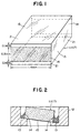
- Figure 1 of the accompanying drawing is a perspective view of a polarizer 11 or analyzer 17 in the configuration of a rectangular parallelepiped or rectangular plate having six surfaces 21, 21, 21, 21, 15, 15, of which at least two of the four side surfaces 21 are subjected to metallization and the grained areas 14 on the side surface 21 defined by excepting the upper and lower very narrow linear areas of each 100 ⁇ m width are the areas for actual metallization.
- the material forming the polarizer and analyzer is preferably polarizing glass which is not particularly limitative provided that the surface thereof has polarizability as exemplified by the commercial product of Polacore ( supra ).
- the thickness of the polarizer 11 or analyzer 17 is preferably in the range from 0.3 mm to 0.6 mm.
- the polarizer 11 or analyzer 17 illustrated in Figure 1 has a thickness of 0.5 mm.
- the metallized area 14 is preferably at least two thirds large of the overall area of the side surface 21.
- the bonding strength cannot be high enough not to accomplish high reliability of the optical isolator.
- metallization is effected on at least two of the four side surfaces 21 or, namely, on the two opposite surfaces 21 or on all of the four side surfaces 21 excepting the top and bottom surfaces 15.
- two metallized areas 14 are on the two opposite side surfaces 21.
- the overall area of metallization in the polarizer 11 or analyzer 17 illustrated in Figure 1 is at least 0.56 mm 2 which is two thirds of maximum metallizable area on two opposite side surfaces 21, i.e, 1.4 ⁇ 0.3 ⁇ 2 ⁇ 2/3 mm2, and cannot exceed 1.68 mm 2 which is the sum of the metallizable areas 14 on all of the four side surfaces 21, i.e. 1.4 ⁇ 0.3 ⁇ 4 mm 2 .
- the method for the metallization is not particularly limitative and, for example, a three-layered structure consisting of chromium, platinum and gold having a thickness of 0.5 to 5 ⁇ m can be formed by the method of vacuum vapor-phase deposition, sputtering or chemical vapor-phase deposition.
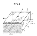
- Figure 2 is a schematic illustration of a polarizer 11 or analyzer 17 bonded to a holder ring 12 by using a solder alloy 13 on the metallized areas 14 according to the invention by a cross sectional view.
- solder or brazing alloy used in bonding of the polarizer or analyzer to the respective holder rings is not particularly limitative including, preferably, a gold-tin alloy and gold-germanium alloy. These solder alloys are preferable in respects of little troubles due to crack formation, high bonding strength to withstand the impact test of the optical isolator and absence of any adverse influences on the quenching ratio at the center and the lowest quenching ratio within the plane to ensure high performance of the optical isolator if not to mention that these alloys are free from the problem of environmental pollution due to toxicity of heavy metals such as lead contained in the solder alloy.
- the material of the holder ring is preferably a Kovar alloy or an iron-nickel alloy because these alloys have a thermal expansion coefficient close to that of the polarizing glass, e.g., 6.5 ⁇ 10 -6 /K, not to cause troubles due to crack formation after bonding by soldering.
- the above mentioned Kovar alloy is an alloy consisting, for example, of 29% by weight of nickel, 17% by weight of cobalt and the balance of iron and having a thermal expansion coefficient of 4.7x10 -6 /K.
- suitable iron-nickel alloy includes the Fe-32Ni alloy consisting of 68% by weight of iron and 32% by weight of nickel and having a thermal expansion coefficient of 6.5 x 10 -6 /K and Fe-42Ni alloy consisting of 58% by weight of iron and 42% by weight of nickel and having a thermal expansion coefficient of 6.5 x 10 -6 /K.
- a grade of stainless steel SUS 340 has a thermal expansion coefficient of 20 x 10 -6 /K so that the stainless steel is less preferable as the material of the holder rings than the above mentioned Kovar alloy and iron-nickel alloys.
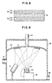
- Figure 4 is a plot showing the distribution of the quenching ratio within the plane of the polariser or analyser prepared in Example 1 described below which indicates that the quenching ratio even at the measuring point in the proximity of the soldered areas is approximately equal to the sufficiently large value at the centre suggesting that the polariser and analyser can be very compact.
- a polarizer and an analyzer of optical glass were subjected to metallization to form a 3 ⁇ m thick metallized layer having a three-layered structure of chromium, platinum and gold in the following manner.
- Figure 1 illustrates a perspective view of a polarizer 11 or analyzer 17 provided with a metallized layer 14 shown by the grained area.
- the polarizer 11 or analyzer 17 was made from polarizing glass (Polacore, supra) and had dimensions of 1.4 mm by 1.4 mm by 0.5 mm.
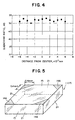
- Two opposite side surfaces 21 were metallized each on the 1.4 mm by 0.30 mm wide area leaving the 0.10 mm wide narrow linear zones from the top and bottom surfaces 15, 15 as is shown in the figure so that the overall metallized area was 0.84 mm 2 .
- Figure 2 schematically illustrates a cross sectional view of a construction consisting of the polarizer 11 or analyzer 17 of the polarizing glass Polacore and a holder ring 12 of a Kovar alloy bonded together by using a gold-tin solder alloy 13 at a temperature of 300 °C in an electric furnace.
- the thus prepared optical isolator was subjected to evaluation tests to find that it was free from cracks as inspected with an optical microscope and could withstand the impact test undertaken under the conditions of 2000 G and 0.3 msecond.
- Table 1 summarizes the overall metallized area in mm 2 , quenching ratio at the center point P and lowest quenching ratio within the plane which is the lowest value of the quenching ratios obtained by measuring the quenching ratio along the chain line L on the top surface of the polarizer 11 or analyzer 17 shown in Figure 3.
- the experimental procedure was substantially the same as in Example 1 except that the holder ring 12 was made from a Fe-32Ni alloy instead of the Kovar alloy.
- the optical isolator was free from cracks and could withstand the impact test.
- the results obtained by the measurement of the quenching ratio are shown in Table 1 below.
- the experimental procedure was substantially the same as in Example 1 except that the holder ring 12 was made from a Fe-42Ni alloy instead of the Kovar alloy.
- the optical isolator was free from cracks and could withstand the impact test.
- the results obtained by the measurement of the quenching ratio are shown in Table 1 below.
- the experimental procedure was substantially the same as in Example 1 except that the metallization was effected on the 1.4 mm by 0.2 mm areas leaving linear areas of 0.15 mm width from the top and bottom surfaces unmetallized.
- the optical isolator was free from cracks and could withstand the impact test.
- the results obtained by the measurement of the quenching ratio are shown in Table 1 below.
- the experimental procedure was substantially the same as in Example 1 except that the metallization was effected on all of the four side surfaces each over a 1.4 mm by 0.3 mm area leaving 0.15 mm wide linear areas from the top and bottom surfaces unmetallized.
- the optical isolator was free from cracks and could withstand the impact test.
- the results obtained by the measurement of the quenching ratio are shown in Table 1 below.
- the experimental procedure was substantially the same as in Example 1 except that the gold-tin solder alloy was replaced with a gold-germanium solder alloy and soldering was performed at 380 °C.
- the optical isolator was free from cracks and could withstand the impact test.
- the results obtained by the measurement of the quenching ratio are shown in Table 1 below.
- the experimental procedure was substantially the same as in Example 1 except that metallization was effected only on the four equilateral right-angled triangular corner areas 14A of the top surface 15 as is shown in Figure 5 instead of the two rectangular areas 14 on the side surfaces.
- the optical isolator was free from cracks and could withstand the impact test.
- Table 1 The results obtained by the measurement of the quenching ratio are shown in Table 1 below.
- Example 1 The experimental procedure was substantially the same as in Example 1 except that metallization was effected allover the 1.4 mm by 0.5 mm wide areas of two opposite side surfaces 21 without leaving the 0.1 mm wide linear zones unmetallized.
- the optical isolator was free from cracks and could withstand the impact test.
- the results obtained by the measurement of the quenching ratio are shown in Table 1.
- the experimental procedure was substantially the same as in Example 1 except that the holder ring 12 was prepared from stainless steel SUS 304 instead of the Kovar alloy.
- the results of the evaluation tests of the optical isolator were that cracks were found in the polarizer and analyzer although the optical isolator could withstand the impact test.
- the results obtained by the measurement of the quenching ratio are shown in Table 1.
- the experimental procedure was substantially the same as in Example 1 except that metallization was effected over the 1.4 mm by 0.10 mm wide areas on the two opposite side surfaces 21, 21 leaving 0.20 mm wide linear zones from the top and bottom surfaces 15, 15 unmetallized.
- the results of the evaluation tests of the optical isolator were that, although no cracks were found in the polarizer and analyzer, the optical isolator could not withstand the impact test.
- the results obtained by the measurement of the quenching ratio are shown in Table 1.
- Figure 4 shows the distribution of the quenching ratio within the plane as measured in Example 1 along the center line L shown in Figure 3 on the top surface 15 of the polarizer 11 or analyzer 17, from which it is understood that the quenching ratio is uniform allover the surface with a value at the solder-bonded portions approximately equal to the large value at the center point P.
- an optical isolator can be constructed with very compact polarizer and analyzer.
- Examples 1 and 6 indicate that the gold-tin alloy and gold-germanium alloy as the solder alloy are preferred in respect of absence of the troubles due to crack formation and the large quenching ratio of the optical isolator which can withstand the impact test by virtue of the good bonding strength therewith.
Landscapes
- Physics & Mathematics (AREA)
- General Physics & Mathematics (AREA)
- Optics & Photonics (AREA)
- Chemical & Material Sciences (AREA)
- Inorganic Chemistry (AREA)
- Nonlinear Science (AREA)
- Engineering & Computer Science (AREA)
- Power Engineering (AREA)
- Optical Elements Other Than Lenses (AREA)
- Surface Treatment Of Optical Elements (AREA)
Claims (6)
- Moyen d'isolation optique comprenant un polariseur (11), un analyseur (17), un rotateur de Faraday et un aimant permanent agencés dans un support possédant des anneaux de support (12) pour un réglage en position du polariseur et analyseur, dans lequel une couche métallisée (14) est formée sur au moins deux surfaces (21) du polariseur et analyseur à travers laquelle un trajet optique ne traverse pas le moyen d'isolation optique en utilisation et le polariseur et analyseur est lié aux anneaux de support correspondants par soudage à l'aide d'un alliage de soudure (13) avec interposition de la couche métallisée correspondante entre le polariseur et analyseur et l'anneau de support correspondant,
caractérisé en ce que les polariseur et analyseur sont fabriqués à partir d'un verre polarisant, les anneaux de support sont fabriqués à partir d'un alliage de Kovar ou d'un alliage de fer et de nickel, et la ou chaque couche métallisée est formée sur la zone de la surface correspondante à l'exception des zones linéaires possédant une largeur de 50 µm à 150 µm, adjacentes aux surfaces (15) du polariseur ou analyseur à travers lesquelles un trajet optique passe lorsque le moyen d'isolation optique est en utilisation. - Moyen d'isolation optique selon la revendication 1, dans lequel l'alliage de soudure est un alliage d'or et d'étain ou un alliage d'or ou de germanium.
- Moyen d'isolation optique selon la revendication 1 ou 2, dans lequel la ou chaque couche métallisée est d'au moins les deux tiers de la zone globale de la surface correspondante.
- Moyen d'isolation optique selon l'une quelconque des revendications précédentes, dans lequel la couche métallisée possède une structure multicouche comprenant du chrome, du platine et de l'or.
- Moyen d'isolation optique selon l'une quelconque des revendications précédentes, dans lequel la ou chaque couche métallisée possède une épaisseur comprise entre 0,5 µm et 5 µm.
- Moyen d'isolation optique selon l'une quelconque des revendications précédentes, dans lequel la ou chaque dite zone linéaire possède une largeur comprise entre 80 µm et 120 µm.
Priority Applications (1)
| Application Number | Priority Date | Filing Date | Title |
|---|---|---|---|
| EP00113469A EP1072925B1 (fr) | 1995-12-18 | 1996-12-17 | Element optique ayant une couche antiréfléchissante résistante à la chaleur |
Applications Claiming Priority (6)
| Application Number | Priority Date | Filing Date | Title |
|---|---|---|---|
| JP328494/95 | 1995-12-18 | ||
| JP32849495 | 1995-12-18 | ||
| JP32849495 | 1995-12-18 | ||
| JP1566/96 | 1996-01-09 | ||
| JP156696 | 1996-01-09 | ||
| JP8001566A JPH09189801A (ja) | 1996-01-09 | 1996-01-09 | 耐熱性反射防止膜付き光学部品 |
Related Child Applications (1)
| Application Number | Title | Priority Date | Filing Date |
|---|---|---|---|
| EP00113469A Division EP1072925B1 (fr) | 1995-12-18 | 1996-12-17 | Element optique ayant une couche antiréfléchissante résistante à la chaleur |
Publications (3)
| Publication Number | Publication Date |
|---|---|
| EP0780717A2 EP0780717A2 (fr) | 1997-06-25 |
| EP0780717A3 EP0780717A3 (fr) | 1999-05-06 |
| EP0780717B1 true EP0780717B1 (fr) | 2001-11-14 |
Family
ID=26334809
Family Applications (2)
| Application Number | Title | Priority Date | Filing Date |
|---|---|---|---|
| EP96309199A Expired - Lifetime EP0780717B1 (fr) | 1995-12-18 | 1996-12-17 | Isolateur optique et élément optique avec un revêtement résistant à la chaleur et anti-réfléchissant |
| EP00113469A Expired - Lifetime EP1072925B1 (fr) | 1995-12-18 | 1996-12-17 | Element optique ayant une couche antiréfléchissante résistante à la chaleur |
Family Applications After (1)
| Application Number | Title | Priority Date | Filing Date |
|---|---|---|---|
| EP00113469A Expired - Lifetime EP1072925B1 (fr) | 1995-12-18 | 1996-12-17 | Element optique ayant une couche antiréfléchissante résistante à la chaleur |
Country Status (3)
| Country | Link |
|---|---|
| US (2) | US5872652A (fr) |
| EP (2) | EP0780717B1 (fr) |
| DE (2) | DE69616957T2 (fr) |
Families Citing this family (6)
| Publication number | Priority date | Publication date | Assignee | Title |
|---|---|---|---|---|
| JP2002511974A (ja) * | 1997-06-26 | 2002-04-16 | コーニング インコーポレイテッド | 光学素子およびそれらの組立て方法 |
| DE29814074U1 (de) * | 1998-08-07 | 1999-12-09 | Pfeifer Seil- und Hebetechnik GmbH & Co, 87700 Memmingen | Preßfitting aus Stahl |
| US7187496B2 (en) * | 2002-03-14 | 2007-03-06 | Tdk Corporation | Manufacturing method of optical device, optical device, manufacturing method of faraday rotator, and optical communication system |
| US20040101226A1 (en) * | 2002-11-26 | 2004-05-27 | Eric Zbinden | Magnet isolator with integrated focusing apparatus |
| JP2009244583A (ja) * | 2008-03-31 | 2009-10-22 | Konica Minolta Opto Inc | 光学素子の製造方法、光学素子ユニット及び撮像ユニット |
| US20100102025A1 (en) * | 2008-10-28 | 2010-04-29 | Essilor International (Compagnie Generale D'optique) | Method and apparatus for marking coated ophthalmic substrates or lens blanks having one or more electrically conductive layers |
Family Cites Families (22)
| Publication number | Priority date | Publication date | Assignee | Title |
|---|---|---|---|---|
| US4194022A (en) * | 1977-07-25 | 1980-03-18 | Ppg Industries, Inc. | Transparent, colorless, electrically conductive coating |
| US4509880A (en) * | 1981-03-30 | 1985-04-09 | Honeywell Inc. | Very high hermeticity glass to metal seal |
| US4732454A (en) * | 1985-04-22 | 1988-03-22 | Toray Industries, Inc. | Light-transmissible plate shielding electromagnetic waves |
| JPH0750262B2 (ja) * | 1988-02-04 | 1995-05-31 | 富士電気化学株式会社 | 光アイソレータの製造方法 |
| JP2995747B2 (ja) * | 1989-05-16 | 1999-12-27 | 日本電気株式会社 | 光アイソレータ内蔵半導体レーザモジュール |
| JP2686453B2 (ja) * | 1989-09-27 | 1997-12-08 | 信越化学工業 株式会社 | 光アイソレータ |
| US5170291A (en) * | 1989-12-19 | 1992-12-08 | Leybold Aktiengesellschaft | Coating, composed of an optically effective layer system, for substrates, whereby the layer system has a high anti-reflective effect, and method for manufacturing the coating |
| JP2967157B2 (ja) * | 1990-03-08 | 1999-10-25 | 信越化学工業株式会社 | 光アイソレータ |
| US5341235A (en) * | 1990-04-18 | 1994-08-23 | Shin-Etsu Chemical Co., Ltd. | Optical isolator and method for preparing same |
| JP2628774B2 (ja) * | 1990-04-20 | 1997-07-09 | 株式会社日立製作所 | 光アイソレータ内蔵形半導体レーザモジュール |
| JPH0511215A (ja) | 1991-07-02 | 1993-01-19 | Tokin Corp | 光アイソレータ |
| JP2567358Y2 (ja) | 1991-08-22 | 1998-04-02 | 株式会社トーキン | 光アイソレータ |
| JP2596801Y2 (ja) | 1992-05-28 | 1999-06-21 | 信越化学工業株式会社 | 光アイソレータ |
| JP3413219B2 (ja) | 1992-07-20 | 2003-06-03 | エヌイーシートーキン株式会社 | 光アイソレータ用光学素子の接着方法 |
| JPH0667119A (ja) | 1992-08-24 | 1994-03-11 | Tokin Corp | 光アイソレータの作製方法 |
| JP3267711B2 (ja) | 1992-11-30 | 2002-03-25 | 株式会社トーキン | 光アイソレータ |
| US5578377A (en) * | 1993-04-21 | 1996-11-26 | Asahi Glass Company Ltd. | Colored thin film-forming coating solution and colored thin film obtained by such coating solution |
| JP3347467B2 (ja) * | 1993-04-21 | 2002-11-20 | 旭硝子株式会社 | 着色薄膜形成用塗布液、着色薄膜とその製造方法、およびガラス物品 |
| DE4431285C1 (de) * | 1994-09-02 | 1995-12-07 | Ant Nachrichtentech | Lasermodul |
| JP3439275B2 (ja) * | 1994-11-25 | 2003-08-25 | エヌイーシートーキン株式会社 | 光アイソレータの製造方法 |
| KR0176767B1 (ko) * | 1995-03-17 | 1999-05-01 | 구자홍 | 다이아몬드상 탄소 박막의 반사 방지 층을 갖는 액정 표시 장치 |
| US5719705A (en) * | 1995-06-07 | 1998-02-17 | Sola International, Inc. | Anti-static anti-reflection coating |
-
1996
- 1996-12-17 DE DE69616957T patent/DE69616957T2/de not_active Expired - Fee Related
- 1996-12-17 EP EP96309199A patent/EP0780717B1/fr not_active Expired - Lifetime
- 1996-12-17 EP EP00113469A patent/EP1072925B1/fr not_active Expired - Lifetime
- 1996-12-17 DE DE69631495T patent/DE69631495D1/de not_active Expired - Lifetime
- 1996-12-17 US US08/768,292 patent/US5872652A/en not_active Expired - Fee Related
-
1998
- 1998-11-17 US US09/193,128 patent/US6163404A/en not_active Expired - Fee Related
Also Published As
| Publication number | Publication date |
|---|---|
| DE69616957D1 (de) | 2001-12-20 |
| DE69616957T2 (de) | 2002-06-27 |
| US5872652A (en) | 1999-02-16 |
| US6163404A (en) | 2000-12-19 |
| DE69631495D1 (de) | 2004-03-11 |
| EP1072925B1 (fr) | 2004-02-04 |
| EP0780717A3 (fr) | 1999-05-06 |
| EP1072925A3 (fr) | 2001-08-22 |
| EP1072925A2 (fr) | 2001-01-31 |
| EP0780717A2 (fr) | 1997-06-25 |
Similar Documents
| Publication | Publication Date | Title |
|---|---|---|
| US5864427A (en) | Polarizer and production method thereof | |
| US6861272B2 (en) | Optical device free from stress due to difference in thermal expansion coefficient between parts and process for fabrication thereof | |
| DE60130471T2 (de) | Sensor für ultrareine und stark korrosive umgebungen | |
| US4876893A (en) | Strain gauges for the pressure sensor | |
| EP0780717B1 (fr) | Isolateur optique et élément optique avec un revêtement résistant à la chaleur et anti-réfléchissant | |
| CA1143024A (fr) | Traversee electrique etanche | |
| EP1008567B1 (fr) | Procede permettant de coller des elements en verre | |
| US6275336B1 (en) | Optical isolator | |
| EP0742467B1 (fr) | Procede de production d'isolateur optique | |
| US5428996A (en) | Hinge assembly for integrated accelerometer | |
| US6462872B2 (en) | Optical isolator | |
| JP3678860B2 (ja) | 光アイソレータ | |
| JPH10227996A (ja) | 光アイソレータ | |
| JP3413219B2 (ja) | 光アイソレータ用光学素子の接着方法 | |
| GB2095604A (en) | Seal between two components | |
| JP3100213B2 (ja) | 光アイソレータ | |
| JP2004354646A (ja) | 光アイソレータおよびその組立方法 | |
| JP4491530B2 (ja) | 光アイソレータ | |
| CN1071041C (zh) | 薄膜磁头及其制造方法 | |
| FR2752054A1 (fr) | Dispositif de mesure de temperature | |
| JP3347198B2 (ja) | 光アイソレータの作製方法 | |
| Vianco et al. | Solder bond applications in a piezoelectric sensor assembly | |
| JPH03179317A (ja) | 光アイソレータ用ファラデー回転子及びそのメタライズ法 | |
| JPH08271835A (ja) | 光アイソレータ | |
| JP2529484Y2 (ja) | 光アイソレータ |
Legal Events
| Date | Code | Title | Description |
|---|---|---|---|
| PUAI | Public reference made under article 153(3) epc to a published international application that has entered the european phase |
Free format text: ORIGINAL CODE: 0009012 |
|
| AK | Designated contracting states |
Kind code of ref document: A2 Designated state(s): DE FR GB |
|
| PUAL | Search report despatched |
Free format text: ORIGINAL CODE: 0009013 |
|
| AK | Designated contracting states |
Kind code of ref document: A3 Designated state(s): DE FR GB |
|
| 17P | Request for examination filed |
Effective date: 19991025 |
|
| 17Q | First examination report despatched |
Effective date: 20000210 |
|
| GRAG | Despatch of communication of intention to grant |
Free format text: ORIGINAL CODE: EPIDOS AGRA |
|
| GRAG | Despatch of communication of intention to grant |
Free format text: ORIGINAL CODE: EPIDOS AGRA |
|
| GRAG | Despatch of communication of intention to grant |
Free format text: ORIGINAL CODE: EPIDOS AGRA |
|
| GRAH | Despatch of communication of intention to grant a patent |
Free format text: ORIGINAL CODE: EPIDOS IGRA |
|
| GRAH | Despatch of communication of intention to grant a patent |
Free format text: ORIGINAL CODE: EPIDOS IGRA |
|
| GRAA | (expected) grant |
Free format text: ORIGINAL CODE: 0009210 |
|
| AK | Designated contracting states |
Kind code of ref document: B1 Designated state(s): DE FR GB |
|
| REF | Corresponds to: |
Ref document number: 69616957 Country of ref document: DE Date of ref document: 20011220 |
|
| REG | Reference to a national code |
Ref country code: GB Ref legal event code: IF02 |
|
| PLBE | No opposition filed within time limit |
Free format text: ORIGINAL CODE: 0009261 |
|
| STAA | Information on the status of an ep patent application or granted ep patent |
Free format text: STATUS: NO OPPOSITION FILED WITHIN TIME LIMIT |
|
| 26N | No opposition filed | ||
| PGFP | Annual fee paid to national office [announced via postgrant information from national office to epo] |
Ref country code: FR Payment date: 20031210 Year of fee payment: 8 |
|
| PGFP | Annual fee paid to national office [announced via postgrant information from national office to epo] |
Ref country code: DE Payment date: 20031229 Year of fee payment: 8 |
|
| PG25 | Lapsed in a contracting state [announced via postgrant information from national office to epo] |
Ref country code: DE Free format text: LAPSE BECAUSE OF NON-PAYMENT OF DUE FEES Effective date: 20050701 |
|
| PG25 | Lapsed in a contracting state [announced via postgrant information from national office to epo] |
Ref country code: FR Free format text: LAPSE BECAUSE OF NON-PAYMENT OF DUE FEES Effective date: 20050831 |
|
| REG | Reference to a national code |
Ref country code: FR Ref legal event code: ST |
|
| PGFP | Annual fee paid to national office [announced via postgrant information from national office to epo] |
Ref country code: GB Payment date: 20061213 Year of fee payment: 11 |
|
| GBPC | Gb: european patent ceased through non-payment of renewal fee |
Effective date: 20071217 |
|
| PG25 | Lapsed in a contracting state [announced via postgrant information from national office to epo] |
Ref country code: GB Free format text: LAPSE BECAUSE OF NON-PAYMENT OF DUE FEES Effective date: 20071217 |