EP0780962B1 - Elektronisch kommutierter Motor - Google Patents
Elektronisch kommutierter Motor Download PDFInfo
- Publication number
- EP0780962B1 EP0780962B1 EP96119750A EP96119750A EP0780962B1 EP 0780962 B1 EP0780962 B1 EP 0780962B1 EP 96119750 A EP96119750 A EP 96119750A EP 96119750 A EP96119750 A EP 96119750A EP 0780962 B1 EP0780962 B1 EP 0780962B1
- Authority
- EP
- European Patent Office
- Prior art keywords
- motor
- microprocessor
- reset
- input
- capacitor
- Prior art date
- Legal status (The legal status is an assumption and is not a legal conclusion. Google has not performed a legal analysis and makes no representation as to the accuracy of the status listed.)
- Expired - Lifetime
Links
- 239000003990 capacitor Substances 0.000 claims description 38
- 125000004122 cyclic group Chemical group 0.000 claims description 6
- 230000006870 function Effects 0.000 claims description 6
- 230000001419 dependent effect Effects 0.000 claims description 3
- 210000000352 storage cell Anatomy 0.000 claims 2
- 238000000034 method Methods 0.000 description 17
- 230000008569 process Effects 0.000 description 16
- 238000010586 diagram Methods 0.000 description 5
- 238000013021 overheating Methods 0.000 description 4
- 230000009471 action Effects 0.000 description 3
- 230000008901 benefit Effects 0.000 description 2
- 230000007257 malfunction Effects 0.000 description 2
- 230000004048 modification Effects 0.000 description 2
- 238000012986 modification Methods 0.000 description 2
- 238000004804 winding Methods 0.000 description 2
- 230000003213 activating effect Effects 0.000 description 1
- 230000000903 blocking effect Effects 0.000 description 1
- 239000000919 ceramic Substances 0.000 description 1
- 230000008859 change Effects 0.000 description 1
- 230000007423 decrease Effects 0.000 description 1
- 230000007547 defect Effects 0.000 description 1
- 230000002950 deficient Effects 0.000 description 1
- 230000001934 delay Effects 0.000 description 1
- 238000011161 development Methods 0.000 description 1
- 230000018109 developmental process Effects 0.000 description 1
- 230000004069 differentiation Effects 0.000 description 1
- 230000005611 electricity Effects 0.000 description 1
- 230000003993 interaction Effects 0.000 description 1
- 230000001681 protective effect Effects 0.000 description 1
- 230000004044 response Effects 0.000 description 1
- 230000001052 transient effect Effects 0.000 description 1
- 230000001960 triggered effect Effects 0.000 description 1
Images




Classifications
-
- H—ELECTRICITY
- H02—GENERATION; CONVERSION OR DISTRIBUTION OF ELECTRIC POWER
- H02P—CONTROL OR REGULATION OF ELECTRIC MOTORS, ELECTRIC GENERATORS OR DYNAMO-ELECTRIC CONVERTERS; CONTROLLING TRANSFORMERS, REACTORS OR CHOKE COILS
- H02P23/00—Arrangements or methods for the control of AC motors characterised by a control method other than vector control
- H02P23/0077—Characterised by the use of a particular software algorithm
-
- H—ELECTRICITY
- H02—GENERATION; CONVERSION OR DISTRIBUTION OF ELECTRIC POWER
- H02P—CONTROL OR REGULATION OF ELECTRIC MOTORS, ELECTRIC GENERATORS OR DYNAMO-ELECTRIC CONVERTERS; CONTROLLING TRANSFORMERS, REACTORS OR CHOKE COILS
- H02P6/00—Arrangements for controlling synchronous motors or other dynamo-electric motors using electronic commutation dependent on the rotor position; Electronic commutators therefor
- H02P6/34—Modelling or simulation for control purposes
-
- H—ELECTRICITY
- H02—GENERATION; CONVERSION OR DISTRIBUTION OF ELECTRIC POWER
- H02H—EMERGENCY PROTECTIVE CIRCUIT ARRANGEMENTS
- H02H7/00—Emergency protective circuit arrangements specially adapted for specific types of electric machines or apparatus or for sectionalised protection of cable or line systems, and effecting automatic switching in the event of an undesired change from normal working conditions
- H02H7/08—Emergency protective circuit arrangements specially adapted for specific types of electric machines or apparatus or for sectionalised protection of cable or line systems, and effecting automatic switching in the event of an undesired change from normal working conditions for dynamo-electric motors
- H02H7/093—Emergency protective circuit arrangements specially adapted for specific types of electric machines or apparatus or for sectionalised protection of cable or line systems, and effecting automatic switching in the event of an undesired change from normal working conditions for dynamo-electric motors against increase beyond, or decrease below, a predetermined level of rotational speed
Definitions
- the invention relates to an electronically commutated motor with control of Functions by a microprocessor or microcontroller, in the following Called microprocessor.
- EP-A1-0 540 417 describes an electronically commutated motor with a Current limit known that the type of an electronic fuse Current in the motor cuts out if it gets too high.
- this object is achieved by an electronic commutated motor according to claim 1.
- Watchdog timers are in Known with microprocessors, and it is common to this from Microprocessor, as long as it works properly, reset pulses feed. A safeguard against malfunctions of the microprocessor is but not connected with it, because it may very well be that the Microprocessor continues to issue reset pulses, but at one of its Outputs a defect is present, which then leads to overheating of the latter Output controlled motor leads.
- the reset pulses according Claim 1 does not come from the microprocessor as usual, but from the motor and triggered by its rotation, the security of the entire arrangement significantly increased, because if for what reasons anyway, the engine stops running, the reset pulses are missing, and the watchdog timer is activated.
- the watchdog timer therefore only comes into action when the engine speed falls below the specified value falls, or when the engine has come to a standstill. And it interrupts periodically in the activated state and without switching on of the microprocessor the stator current of the motor.
- Such a motor is preferably further developed according to claim 2.
- the low duty cycle creates long pauses in which there is no electricity flows in the engine so that the risk of engine overheating is eliminated.
- ECM electronically commutated motor
- the invention is suitable for any type of motor, and this motor can also be a collector motor, provided that it generates control impulses during its rotation, for example by a tachometer generator or a Hall generator arranged in or on the motor.
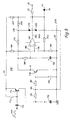
- the permanent magnetic rotor of motor 20 is shown schematically at 22 indicated, and the two strands of its stator winding have the Reference numerals 24 and 26. These are, as shown, on a positive line 28 connected, e.g. + 12 V, + 24 V or + 48 V compared to the Potential of a negative line 30 may have.
- An npn Darlington transistor 32 is used to control the current i 1 in the strand 24, and a corresponding transistor 34 for controlling the current i 2 in the strand 26, both of which are provided with a free-wheeling diode 32 'and 34'.
- the emitters of both transistors 32, 34 are connected to the negative line 30, their collectors to the strands 24 and 26, respectively.
- the base of the transistor 32 is from an AND gate 38 through a Resistor 40 driven, as well as the base of transistor 34 by one AND gate 42 via a resistor 44.
- An input of the AND gate 38 is one with output C1 Microprocessor 50 connected, the other via a resistor 48 a positive supply line 52 of e.g. + 5 V, as well corresponding input of the AND gate 42, and the anode of a diode 54, the cathode of which is connected to the output 58 of an operational amplifier 56 connected is.
- the other input of the AND gate 42 is with the output C2 of the microprocessor 50 connected.
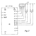
- the individual connections of the microprocessor 50 here a 4-bit microprocessor 17P103 (manufacturer NEC) are shown in Fig. 2 shown schematically. As you can see, the connections B0, B1, B2, C0, C3, D0, D1, D2 each through a resistor R to the positive line 52 (+5 V) connected. This resistance R can e.g. a value of 47 k ⁇ to have.
- a Hall IC 60 is arranged, which in FIG is shown again on the left-hand side below, and that in operation rectangular pulses "Hall" generated, which is shown schematically in Fig. 1 are.
- These are connected via a resistor 62 to the input D3 of the Microprocessor 50 supplied, further via a first differentiator (Resistor 64 and capacitor 66) the reset input RESET / des Microprocessor 50, and via a second differentiating element (capacitor 68, Resistor 70) of the base 71 of an NPN transistor 72, the emitter of which the minus line 30 and its collector with the minus input 74 of Operational amplifier 56 is connected.
- a resistor 62 to the input D3 of the Microprocessor 50 supplied, further via a first differentiator (Resistor 64 and capacitor 66) the reset input RESET / des Microprocessor 50, and via a second differentiating element (capacitor 68, Resistor 70) of the base 71 of an NPN transistor
- a capacitor 76 is between this input 74 and the negative line 30 arranged, and a resistor 78 between this input 74 and the output 58.
- a resistor 80 between the plus input 82 of the operational amplifier 56 and its output 58 arranged, and this plus input 82 is located at the connection point 84 of two resistors 86, 88, of which the former with the positive line 52 and the latter with the Minus line 30 is connected.
- a resistor 90 lies between the output 58 and the positive line 52.
- a resistor 92 connects this output to a node 94 which via a capacitor 96 to the negative line 30 and via a Resistor 98 connected to the reset input 3 of the microprocessor 50 is.
- the input 3 is also connected to the anode of a diode 100, the Cathode is connected to the positive line 52. This prevents the Reset input RESET / assumes a higher potential than the positive line 52.
- a ceramic resonator 102 (8 MHz) is connected to the inputs XIN and XOUT of the microprocessor 50 as the clock generator. Between the input V 00 of the microprocessor 50 and its input GND there is a capacitor 104, which prevents interference pulses from reaching the microprocessor 50 via the positive line 52.
- the Hall signal the frequency of which is proportional to the speed of the motor 20 is input D3 of microprocessor 50 via resistor 62 fed so that the microprocessor to the commutation signals Can properly control outputs C1 and C2, as shown below of the flowchart of FIG. 7 is described and explained in detail.
- Resistor 62 prevents an internal short circuit or Malfunction in the microprocessor 50, the signal Hall is short-circuited and is therefore an important security feature, because without it In this case, resistor 62 would no longer be the cyclical reset process possible.
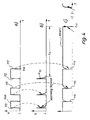
- the signal Hall (FIG. 3a) is differentiated via the capacitor 66 and into differentiated form (FIG. 3b) the input RESET / of the microprocessor 50 fed. With every negative edge 110 of the Hall signal, this becomes Input pulled briefly to 0 V, i.e. to the potential of the Minus line 30, and with every positive edge 112 this input receives RESET / briefly a more positive potential, but as soon as it is 5.7 V exceeds, derived via diode 100 and from capacitor 104 is buffered so that the microprocessor 50 is not affected by this signal is damaged or destroyed.
- Hall IC 60 Since the Hall IC 60 has an open collector output, it has one Pull-up resistor 64, which makes output 61 of Hall IC 60 positive, when its internal output transistor is blocked.
- the capacitor 68 and the resistor 70 form a differentiator that a positive pulse on each positive edge 112 of the Hall signal generated, which makes the transistor 72 briefly conductive, whereby this briefly the minus input 74 of the operational amplifier 56 to 0 V. pulls and discharges the capacitor 76.
- the operational amplifier 56 forms, together with its passive ones Components, a so-called watchdog timer 120, the following is referred to as a WD timer.
- This term is used to refer to a Circuit which is intended to prevent a microprocessor 50 from becoming damaged Glitches or the like "hangs up", somewhere in his Program stops and work is refused.
- the WD timer 120 kicks only in action if he is constantly given so-called refresh impulses which prevent it from becoming active, and these refresh pulses receives it in the present case via the differentiator 68, 70 and transistor 72.
- Fig. 4 shows the procedure just described.
- the Hall signals are shown as the speed decreases. Their positive edges 112 cause the positive pulses u 71 shown in FIG. 4b at the base 71 of the transistor 72, and these pulses cause the capacitor 76 to be continuously discharged as long as the motor 20 is running, ie the motor 20 as long as it is running the refresh signals for the WD timer 120, so that it cannot be activated while the engine 20 is running.
- the Impulse Hall arises again Periodically discharge capacitor 76 and disable WD timer 120.
- the cycle described is repeated, i.e. the WD timer 120 oscillates at a very low frequency, e.g. 0.2 Hz, continuously gives reset pulses to the microprocessor 50, and switches transistor 32 or 34, e.g. one second and four seconds so that the motor 20 cannot overheat, but again starts when the blocking has been removed. This is called one Anti-lock device with automatic restart.
- a PWM signal could be at point P1, that is, the anode of diode 54 feed from a PWM actuator 122, and then you would Set the duty cycle of this PWM actuator 122 to 0% if this Potential at output 58 becomes 0 V.
- This variant is shown in FIG dashed lines indicated; in this case, diode 54 would omitted.
- the PWM controller 122 can be part of a current regulator or one Speed controller (not shown).
- FIG. 5 shows the basic structure of the circuit according to FIG. 1 in the form of a block diagram.
- the Hall IC 60 is coupled to the motor 20 and, when the motor 20 rotates, it supplies refresh pulses to the WD timer 120 via the transistor 72, so that the latter is kept in the non-activated state.
- Hall IC 60 also provides cyclic (via capacitor 66) Reset signals to the microprocessor 50, and a power-up reset takes place at the start through capacitor 96 and resistor 98.
- the microprocessor 50 itself is periodically over when the engine 20 is running reset a cyclic reset process 66, or - when switching on - via the power-up reset 96, 98, or - when the motor 20 is blocked - via the WD timer 120. These alternative possibilities are through a OR symbol symbolizes 130.
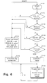
- step S130 the program jumps, controlled by the Address counter of the microprocessor 50, to step S130, where a short if necessary Initialization can take place.
- step S132 it is queried in step S132 whether the memory cell RES_Bit1 is set in the microprocessor 50. If so, you can Program to step S134, where the same query for the internal Memory cell RES_Bit2 takes place. If the answer is positive here, too, it works Program to step S136, where it is queried whether the memory cells for the byte RES_Byte contain the value wxyz.
- step S138 the program may go to step S138, where it is queried whether the Hall signal is high. Because namely according to FIG Cyclic reset only on the negative edge 110 of a Hall signal takes place, the Hall signal must be low after a cyclic reset be, i.e. a high Hall signal means that there is no cyclical reset may have taken place and it is a power-up reset got to. Step S138 may also be omitted if this is already the case Steps S132, 134, 136 are sufficiently safe.
- step S140 turns on cyclical reset process carried out, and in this case none detailed initialization (step S142) is carried out, but it will only the program counter is reset to a certain value and again started, and the flowchart in this case proceeds to step S144, i.e. to the main program with commutation (unless it is a collector motor) and possibly speed control; step S144 is explained below with reference to FIG. 7.
- Steps S132, 134, 136, and possibly 138, of FIG. 6 are one Key system, i.e. the program can only go to step S140, if it has the correct key for the internal memory cells RES_Bit 1, 2 and that has RES_Byte, and this is only the case when in this Memory cells previously loaded certain values. Right after that Switching on is not the case, but then have them Memory cells random values, so that immediately after switching on always at at least one of steps S132 to S136 the answer will be NO. With such a negative answer, the program goes to step S145, i.e. in this case the program automatically recognizes that it is must perform a power-up reset.
- step S145 the internal memory cells RES_Bit1 and 2 is set, and the information wxyz is loaded into the RES_Byte, so that at for each subsequent reset process, queries S132 to S136 with YES are answered and consequently only a cyclical reset process is carried out.
- Step S145 is followed by step S142, where one after switching on extensive initialization is carried out, e.g. Loading a speed setpoint, Querying registers, etc. Then the program goes likewise to step S144, that is to say to the main program, which is in the form here a loop S146 is set up, for the passage of which a constant time is needed, e.g. 80 ⁇ s, and which is run continuously in operation, but interrupted by the cyclical reset processes (S140) in the negative edges 110 of the Hall signal.
- a constant time e.g. 80 ⁇ s
- Fig. 7 shows the structure of the main program.
- the main program is entered, following step S140 or S142 of FIG. 6.
- step S158 e.g. a speed control can take place, or other engine-specific functions.
- step S158 e.g. a speed control can take place, or other engine-specific functions.
- step S152 the program goes through the Loop S146 back to step S152, and this loop S146 is executed in Continuous operation, interrupted only by the cyclical Reset processes (S140) on the negative edges 110 of the Hall signal, by interrupt processes, or by disturbances that a response of the WD timer 120 cause.
- S140 cyclical Reset processes
- the capacitor 76 of the WD timer 120 discharges and only begins during the start-up of the motor 20 charge. Once the motor 20 is running, the capacitor 76 is on the Discharge transistor 72 again and again in the manner described. Thereby normal start-up of motor 20 is possible without the WD timer 120 is activated.
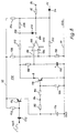
- FIG. 8 shows a variant for the WD timer 120 of FIG. 1.
- This WD timer 170 is activated even at low engine speeds, the stronger the lower the engine speed becomes. It is not activated at normal engine speeds.
- the Hall signals are generated by a differentiator from a capacitor 172 and a resistor 173 of the base of a pnp transistor 174 fed, i.e. at the negative edges 110 of the Hall signal (see FIG. 3a) transistor 174 becomes briefly conductive and carries a capacitor 176 (e.g. 10 nF) between its collector and the negative line 30 is connected to a charging pulse.
- a capacitor 176 e.g. 10 nF
- npn transistor 178 The base of an npn transistor 178 is connected via two resistors 180, 182, whose connection point is designated 184 with the collector of Transistor 174 connected, the emitter of which is connected to the positive line 52 is. Also lies between the base of transistor 178 and the negative line 30 a resistor 186. The emitter of transistor 178 is connected to the Minus line 30 connected, its collector via a resistor 188 (e.g. 10 k) with the minus input 189 of a comparator 190. A capacitor 192 (e.g. 3.3 ⁇ F) lies between the minus input 189 and the Minus line 30. It has the same function as the capacitor 76 of the Fig. 1.
- the plus input 194 of the comparator 190 is via a resistor 196 (e.g. 100 k) with the positive line 52 and via a resistor 198 (e.g. 100 k) connected to the negative line 30.
- a resistor 196 e.g. 100 k
- a resistor 198 e.g. 100 k
- a resistor 202 leads from the output 200 of the comparator 190. to the plus input 194, a resistor 204 (eg 2 k) to the positive line 52, and a resistor 206 (e.g. 470 k) to a node 208.
- a diode 210 lies between output 200 and node 208 (anode at the output 200).
- a resistor 212 (e.g. 100 k) lies between node 208 and the collector of transistor 178.
- transistor 174 is turned on briefly, which causes the Capacitor 176 is charged. This turns on transistor 178 Generated switch-on pulse of defined length, which point B on the Potential of the minus line 30 switches. This will discharge the capacitor 192 through resistor 188.
- capacitor 192 is connected through resistor 204, diode 210, and Resistors 212 and 188 loaded.
- the Hall signal has a high one Frequency so that capacitor 192 is only slightly charged since it is always is discharged again via transistor 178 and resistor 188.
- the minus input 189 of the comparator 190 has a more negative one Potential as the plus input 194, and the comparator 190 is at its Output 200 high impedance, so that it does not trigger a reset and the Diode 54 remains blocked, ie motor 20 runs normally.
- the potential at the plus input 194 should be appropriate (by choosing the Resistors 196, 198) should be set so high that the voltage at Capacitor 192 can span a wide voltage range.
- the point B is less often by the Transistor 178 connected to the negative line 30, and it now predominates Charging capacitor 192 via resistor 204, diode 210 and resistors 212 and 188 so that the negative input 189 of the Comparator 190 becomes more positive than plus input 194. This switches the output 200 to 0 V, there is a WD reset, and the Power stage transistors 32 and 34 (FIG. 1) are blocked via the diode 54.
- the capacitor 192 discharges through the resistors 188, 212 and 206, also additionally by the impulses that continue from the Hall IC 60 (Fig. 1) of the motor still running, so that the OFF time, during which the comparator 190 has the potential 0 V at its output depends on the speed that is still available. The lower this the longer this OFF time, i.e. It is a dynamic overload protection for the motor 20.
- the WD timer 170 according to FIG. 8 has particular advantages when starting up of an engine. It may be that the motor is inhibited when starting up however starts but its speed increases slowly. In this case there the timer 170 more time to reach its operating speed, because via transistor 178, capacitor 192 is turned on again and again partially discharged while the engine is rotating.
- the timer 170 switches at some point the engine off so that it is not overloaded.
- the timer 170 then switches after a predetermined pause turn the engine on again, and the second try is most of the time easier because the engine has already turned. Also shortened the timer 170 automatically sets its OFF time when the engine is running.
- FIG. 9 shows a variant 170 '.
- the output 200 of the comparator 190 is connected to the point 184 via a diode 220, its anode being connected to this point. If the output 200 assumes the potential 0 V, the point 184 is also set to approximately 0 V, so that the transistor 178 can no longer be turned on. In this case, the OFF time is not dependent on the engine speed, but constant.
- Timers 170, 170 ' 8 and 9 can also be used in engines that are not controlled by a microprocessor, but by conventional commutation circuits.
Landscapes
- Engineering & Computer Science (AREA)
- Power Engineering (AREA)
- Control Of Motors That Do Not Use Commutators (AREA)
Description
- Fig. 1
- ein Übersichtsschaltbild eines erfindungsgemäßen elektronisch kommutierten Motors,
- Fig. 2
- eine Darstellung der verschiedenen Anschlüsse eines beim Ausführungsbeispiel verwendeten Mikroprozessors 17P103 der Firma NEC, und der hierfür verwendeten Bezeichnungen,
- Fig. 3 und 4
- Schaubilder zur Erläuterung der Wirkungsweise,
- Fig. 5
- ein Blockschaltbild zur Erläuterung des Zusammenwirkens der verschiedenen Teile der Fig. 1,
- Fig. 6
- ein Flußdiagramm zur Erläuterung, wie bestimmte Resetvorgänge voneinander unterschieden werden,
- Fig. 7
- ein Flußdiagramm zur Erläuterung des Ablaufs der Kommutierung,
- Fig. 8
- ein Schaltbild einer Variante des Watchdog-Zeitglieds, und
- Fig. 9
- eine Variante zu Fig. 8.
Claims (7)
- Elektronisch kommutierter Motor mit Steuerung von Funktionen durch einen Mikroprozessor oder Mikrocontroller (50), im folgenden generell "Mikroprozessor" genannt,
mit einem außerhalb des Mikroprozessors (50) angeordneten Watchdog-Zeitglied (120; 170; 170'), das einen Multivibrator mit niedriger Schwingungsfrequenz enthält,welcher bei laufendem Motor (20) durch bei Drehung des Motors erzeugte Signale, zumindest oberhalb einer vorgegebenen Motordrehzahl, in einem deaktivierten Zustand gehalten wird,und welcher im aktivierten Zustand, periodisch, und ohne Einschaltung des Mikroprozessors (50), den Statorstrom (i1, i2) des Motors (20) unterbricht. - Motor nach Anspruch 1, bei welchem der Multivibrator im aktivierten Zustand den Statorstrom (i1, i2) des Motors (20) mit einem niedrigen Tastverhältnis unterbricht, so daß die durch den Motor fließenden Stromimpulse durch lange Strompausen unterbrochen werden.
- Motor nach Anspruch 1 oder 2, bei welchem der im Watchdog-Zeitglied (120; 170; 170') vorgesehene Multivibrator im aktivierten Zustand periodisch einen Kondensator (96) entlädt, der zu einer Power-Up-Reset-Schaltung (96, 98) des Mikroprozessors (50) gehört und mit einem Reseteingang (RESET/) des Mikroprozessors (50) verbunden ist.
- Motor nach einem oder mehreren der vorhergehenden Ansprüche, bei welchem im Mikroprozessor (50) Speicherzellen (RES_Bit1, RES_Bit2; RES_Byte) vorgesehen sind, welche nach dem Einschalten und vor dem Power-Up-Reset mit Zufallswerten geladen sind und bei einem Resetvorgang abgefragt werden und dann zu einem Power-Up-Reset führen, wenn sie solche zufallsbedingten Werte enthalten, und daß Mittel vorgesehen sind, welche bei einem Power-Up-Resetvorgang diese Speicherzellen mit vorgegebenen Werten laden, so daß ihre Abfrage bei einem von der Drehung des Motors (20) bewirkten Resetvorgang zu einem von einem Power-Up-Reset verschiedenen, zyklischen Resetvorgang führt.
- Motor nach einem oder mehreren der vorhergehenden Ansprüche, bei welchem das Tastverhältnis des Multivibrators im Watchdog-Zeitglied (170) von der Drehzahl des Motors (20) abhängig ist.
- Motor nach Anspruch 5, bei welchem das Tastverhältnis des Watchdog-Zeitglieds (170) bei sich drehendem Motor (20) höher ist als bei blockiertem Motor.
- Motor nach einem oder mehreren der vorhergehenden Ansprüche, bei welchem zur Erfassung der Rotorstellung ein Hall-IC (60) vorgesehen ist, dessen Ausgangssignal über einen Entkopplungswiderstand (62) einem Eingang (D3) des Mikroprozessors (50) zuführbar ist, welcher Entkopplungswiderstand (62) so dimensioniert ist, daß bei einem internen Kurzschluß an diesem Eingang des Mikroprozessors (50) die Arbeitsweise der übrigen, vom Signal des Hall-IC (60) abhängigen Funktionen nicht beeinträchtigt ist.
Applications Claiming Priority (2)
| Application Number | Priority Date | Filing Date | Title |
|---|---|---|---|
| DE19547216 | 1995-12-18 | ||
| DE19547216 | 1995-12-18 |
Publications (3)
| Publication Number | Publication Date |
|---|---|
| EP0780962A2 EP0780962A2 (de) | 1997-06-25 |
| EP0780962A3 EP0780962A3 (de) | 1998-04-08 |
| EP0780962B1 true EP0780962B1 (de) | 2001-02-28 |
Family
ID=7780435
Family Applications (1)
| Application Number | Title | Priority Date | Filing Date |
|---|---|---|---|
| EP96119750A Expired - Lifetime EP0780962B1 (de) | 1995-12-18 | 1996-12-10 | Elektronisch kommutierter Motor |
Country Status (2)
| Country | Link |
|---|---|
| EP (1) | EP0780962B1 (de) |
| DE (2) | DE19650907A1 (de) |
Cited By (1)
| Publication number | Priority date | Publication date | Assignee | Title |
|---|---|---|---|---|
| US6810292B1 (en) | 1999-05-21 | 2004-10-26 | Ebm-Papst St. Georgen Gmbh & Co. Kg | Method for nonvolatile storage of at least one operating data value of an electrical motor, and electrical motor for said method |
Family Cites Families (3)
| Publication number | Priority date | Publication date | Assignee | Title |
|---|---|---|---|---|
| GB9016508D0 (en) * | 1990-07-27 | 1990-09-12 | Papst Motors Limited | Brushless d.c.motors |
| FR2683406B1 (fr) * | 1991-10-31 | 1997-07-18 | Valeo Thermique Habitacle | Dispositif de protection contre les surcharges pour moteur electrique a commutation electronique. |
| US5590235A (en) | 1993-12-03 | 1996-12-31 | Papst-Motoren Gmbh & Co. Kg | DC motor control with periodic reset |
-
1996
- 1996-12-07 DE DE19650907A patent/DE19650907A1/de not_active Withdrawn
- 1996-12-10 DE DE59606505T patent/DE59606505D1/de not_active Expired - Lifetime
- 1996-12-10 EP EP96119750A patent/EP0780962B1/de not_active Expired - Lifetime
Cited By (1)
| Publication number | Priority date | Publication date | Assignee | Title |
|---|---|---|---|---|
| US6810292B1 (en) | 1999-05-21 | 2004-10-26 | Ebm-Papst St. Georgen Gmbh & Co. Kg | Method for nonvolatile storage of at least one operating data value of an electrical motor, and electrical motor for said method |
Also Published As
| Publication number | Publication date |
|---|---|
| EP0780962A3 (de) | 1998-04-08 |
| EP0780962A2 (de) | 1997-06-25 |
| DE59606505D1 (de) | 2001-04-05 |
| DE19650907A1 (de) | 1997-06-19 |
Similar Documents
| Publication | Publication Date | Title |
|---|---|---|
| EP0744807B1 (de) | Verfahren zur Strombegrenzung bei einem Gleichstrommotor, und Gleichstrommotor zur Durchführung eines solchen Verfahrens | |
| EP0739084B1 (de) | Verfahren zum Steuern oder Regeln eines Elektromotors, und Anordnung zur Durchführung eines solchen Verfahrens | |
| EP1088387B1 (de) | Anordnung mit einem elektromotor | |
| EP1471628B1 (de) | Elektronisch kommutierter Motor, und Verfahren zum Betreiben eines solchen | |
| EP0895345B1 (de) | Verfahren zur Überwachung eines kollektorlosen Gleichstrommotors, und Motor zur Durchführung eines solchen Verfahrens | |
| EP0658973B1 (de) | Elektronisch kommutierter Elektromotor und Verfahren zu seinem Betrieb | |
| EP0865681B1 (de) | Verfahren zum regeln einer physikalischen grösse, und anordnung zur durchführung eines solchen verfahrens | |
| CH662907A5 (de) | Elektronische kupplung fuer elektrowerkzeuge mit waehlbarer drehzahl. | |
| EP1675757B1 (de) | Vorrichtung und verfahren zum steuern einer gleichspannung | |
| EP1118152B1 (de) | Elektronisch kommutierter motor | |
| DE3115243C2 (de) | ||
| DE19518991A1 (de) | Verfahren zum Betrieb eines elektronisch kommutierten Motors, und Motor zur Durchführung eines solchen Verfahrens | |
| DE3418276C2 (de) | ||
| EP1107441A2 (de) | Elektronisch kommunierter Gleichstrommotor | |
| EP0492103A2 (de) | Einrichtung zur Spannungsversorgung bei Geräten mit Nachlauf | |
| DE3044027C2 (de) | Stromregler für einen Gleichstrommotor | |
| DE3607014B4 (de) | Schaltungsanordnung zur pulsbreitenmodulierten Ansteuerung eines Gleichstrommotors | |
| EP0780962A2 (de) | Elektronisch kommutierter Motor | |
| DE19519248A1 (de) | Verfahren zur Strombegrenzung bei einem Gleichstrommotor, und Gleichstrommotor zur Durchführung eines solchen Verfahrens | |
| EP0713280B1 (de) | Elektronisch kommutierter Motor | |
| EP1142100A1 (de) | Elektronisch kommutierter motor | |
| CH656992A5 (en) | Rotation speed regulating arrangement for a DC motor, and a fan having such an arrangement | |
| DE29606939U1 (de) | Anordnung mit einem PWM-Steller | |
| DE29513783U1 (de) | Elektronisch kommutierter Motor |
Legal Events
| Date | Code | Title | Description |
|---|---|---|---|
| PUAI | Public reference made under article 153(3) epc to a published international application that has entered the european phase |
Free format text: ORIGINAL CODE: 0009012 |
|
| AK | Designated contracting states |
Kind code of ref document: A2 Designated state(s): DE FR GB SE |
|
| RTI1 | Title (correction) | ||
| PUAL | Search report despatched |
Free format text: ORIGINAL CODE: 0009013 |
|
| AK | Designated contracting states |
Kind code of ref document: A3 Designated state(s): DE FR GB SE |
|
| 17P | Request for examination filed |
Effective date: 19980403 |
|
| 17Q | First examination report despatched |
Effective date: 19990603 |
|
| GRAG | Despatch of communication of intention to grant |
Free format text: ORIGINAL CODE: EPIDOS AGRA |
|
| GRAG | Despatch of communication of intention to grant |
Free format text: ORIGINAL CODE: EPIDOS AGRA |
|
| GRAH | Despatch of communication of intention to grant a patent |
Free format text: ORIGINAL CODE: EPIDOS IGRA |
|
| GRAH | Despatch of communication of intention to grant a patent |
Free format text: ORIGINAL CODE: EPIDOS IGRA |
|
| GRAA | (expected) grant |
Free format text: ORIGINAL CODE: 0009210 |
|
| AK | Designated contracting states |
Kind code of ref document: B1 Designated state(s): DE FR GB SE |
|
| PG25 | Lapsed in a contracting state [announced via postgrant information from national office to epo] |
Ref country code: SE Free format text: LAPSE BECAUSE OF FAILURE TO SUBMIT A TRANSLATION OF THE DESCRIPTION OR TO PAY THE FEE WITHIN THE PRESCRIBED TIME-LIMIT Effective date: 20010228 |
|
| REF | Corresponds to: |
Ref document number: 59606505 Country of ref document: DE Date of ref document: 20010405 |
|
| GBT | Gb: translation of ep patent filed (gb section 77(6)(a)/1977) |
Effective date: 20010327 |
|
| ET | Fr: translation filed | ||
| REG | Reference to a national code |
Ref country code: GB Ref legal event code: IF02 |
|
| PLBE | No opposition filed within time limit |
Free format text: ORIGINAL CODE: 0009261 |
|
| STAA | Information on the status of an ep patent application or granted ep patent |
Free format text: STATUS: NO OPPOSITION FILED WITHIN TIME LIMIT |
|
| 26N | No opposition filed | ||
| PGFP | Annual fee paid to national office [announced via postgrant information from national office to epo] |
Ref country code: GB Payment date: 20091223 Year of fee payment: 14 Ref country code: FR Payment date: 20091113 Year of fee payment: 14 |
|
| PGFP | Annual fee paid to national office [announced via postgrant information from national office to epo] |
Ref country code: DE Payment date: 20091201 Year of fee payment: 14 |
|
| GBPC | Gb: european patent ceased through non-payment of renewal fee |
Effective date: 20101210 |
|
| REG | Reference to a national code |
Ref country code: FR Ref legal event code: ST Effective date: 20110831 |
|
| PG25 | Lapsed in a contracting state [announced via postgrant information from national office to epo] |
Ref country code: FR Free format text: LAPSE BECAUSE OF NON-PAYMENT OF DUE FEES Effective date: 20110103 |
|
| REG | Reference to a national code |
Ref country code: DE Ref legal event code: R119 Ref document number: 59606505 Country of ref document: DE Effective date: 20110701 |
|
| PG25 | Lapsed in a contracting state [announced via postgrant information from national office to epo] |
Ref country code: DE Free format text: LAPSE BECAUSE OF NON-PAYMENT OF DUE FEES Effective date: 20110701 Ref country code: GB Free format text: LAPSE BECAUSE OF NON-PAYMENT OF DUE FEES Effective date: 20101210 |