EP0780982A1 - Système d'horloge complémentaire - Google Patents
Système d'horloge complémentaire Download PDFInfo
- Publication number
- EP0780982A1 EP0780982A1 EP96120620A EP96120620A EP0780982A1 EP 0780982 A1 EP0780982 A1 EP 0780982A1 EP 96120620 A EP96120620 A EP 96120620A EP 96120620 A EP96120620 A EP 96120620A EP 0780982 A1 EP0780982 A1 EP 0780982A1
- Authority
- EP
- European Patent Office
- Prior art keywords
- clock
- clock system
- inductive element
- circuit
- complementary clock
- Prior art date
- Legal status (The legal status is an assumption and is not a legal conclusion. Google has not performed a legal analysis and makes no representation as to the accuracy of the status listed.)
- Withdrawn
Links
- 230000000295 complement effect Effects 0.000 title claims description 11
- 230000001939 inductive effect Effects 0.000 claims abstract description 10
- 238000007599 discharging Methods 0.000 claims description 6
- 238000001465 metallisation Methods 0.000 claims description 2
- 239000004065 semiconductor Substances 0.000 claims 3
- 230000000903 blocking effect Effects 0.000 claims 1
- 238000004519 manufacturing process Methods 0.000 claims 1
- 239000003990 capacitor Substances 0.000 abstract description 2
- 230000010355 oscillation Effects 0.000 description 4
- 238000005516 engineering process Methods 0.000 description 3
- 230000005855 radiation Effects 0.000 description 3
- 238000010586 diagram Methods 0.000 description 2
- 230000003139 buffering effect Effects 0.000 description 1
- 239000013078 crystal Substances 0.000 description 1
- 238000013016 damping Methods 0.000 description 1
- 230000003247 decreasing effect Effects 0.000 description 1
- 230000001419 dependent effect Effects 0.000 description 1
- 238000004146 energy storage Methods 0.000 description 1
- 238000000034 method Methods 0.000 description 1
Images

Classifications
-
- H—ELECTRICITY
- H03—ELECTRONIC CIRCUITRY
- H03K—PULSE TECHNIQUE
- H03K17/00—Electronic switching or gating, i.e. not by contact-making and –breaking
- H03K17/16—Modifications for eliminating interference voltages or currents
- H03K17/161—Modifications for eliminating interference voltages or currents in field-effect transistor switches
- H03K17/162—Modifications for eliminating interference voltages or currents in field-effect transistor switches without feedback from the output circuit to the control circuit
Definitions
- the invention relates to a complementary clock system for antiphase clocks, which are used in clocked logic systems with monolithically integrated circuits, in particular CMOS circuits. It is known that very high load currents can flow on the supply lines, the load currents being essentially caused by the constant charging and discharging of the gate capacitances and increasing in direct proportion to the clock frequency. In addition to a high crystal temperature as a result of the power loss, the load currents are particularly unpleasant due to their interference radiation. A capacitive buffering of the current peaks at the outer circuit connections is unsatisfactory because the path over the connection legs is already too long. These difficulties increase with increasing clock frequencies.
- the invention is based on the basic idea that, in the usual driver stages, the charging current for the one load capacity is fed from the positive supply source and the discharge current is derived from the negative supply source or to ground. Almost simultaneously, the discharge or charging current for the other load capacity flows in the opposite direction.
- part of these currents can serve to initially charge or discharge the other load capacity during the switching interval. This is achieved by means of a switchable current path which is inserted between the two clock lines and is switched on at a suitable time interval, that is to say at the start of the charging or discharging. However, this would require a very short and precisely timed gate pulse.
- the circuit arrangement is selected so that an oscillating circuit is formed by the inductance of the switched current path and the load capacitances, the resonance frequency or half the period of which approximately coincides with the duration of the switching edges of the clock. Then the switched current path is switched on for one half oscillation, so that part of the charge stored in one load capacitance can flow into the other load capacitance, the opening time of the resonant circuit loop taking place in the de-energized state as far as possible. The rest of the charging or discharging then takes place through the usual driver stages.
- the driver stages should be separated or decoupled from the supply sources, if possible, so that the resonant circuit is not short-circuited with a low resistance.
- corresponding interrupter or decoupling circuits are not shown in the exemplary embodiment; they are also superfluous if the leads to the driver stages already act as a choke in this frequency range.
- a clock generator 3 supplies antiphase and non-overlapping clock signals t1, t2 via a first and second output 3.1, 3.2 to a first and second driver stage 1,2.
- These each contain a pair of push-pull circuits 1.1, 1.2 and 2.1, 2.2, respectively, which are fed with a low resistance from a positive and negative supply voltage VDD, VSS.
- a clock line is connected to the output of the driver stages and forms the connection to a first and second load capacitance c1, c2.
- the gate capacitances of the connected transistors are represented as substitutes by the load capacitances.
- the load capacitances are charged or discharged by a first or second load current i1, i2, the positive current direction corresponding to the charge.
- the circuit shown in Fig. 2 contains essentially the same elements as Fig. 1, compare also the same reference numerals. Unless there is a match there is no need for another discussion.
- the clock generator 4 has a further output 4.5 for a gate signal t5.
- the circuit contains a switchable current path 5 between the first and second clock lines 9.1, 9.2.
- the current path 5 contains a first inductive element 7.1, a gate circuit 8 and a second inductive element 7.2 in series connection.
- the control input of the gate circuit 8 is connected to the gate signal output 4.5 of the clock generator 4.
- the two inductive elements 7.1, 7.2 together form an inductance L, which is only divided for the better symmetry of the circuit.
- the currents i3, i4 respectively coupled to the driver stages 1, 2 are shown as arrows and define the positive current direction.
- the current through the switched current path 5 is shown for the positive direction as arrow i5.
- the series circuit of the two load capacitances c1, c2, which is simply referred to as capacitance C below forms an oscillating circuit with the inductance L, which is closed via the gate circuit 8 and the common ground connection VSS .
- the size of the load capacitances c1, c2 depends, in addition to the technology, in particular directly on the respective circuit scope. For large circuits, the value can easily be between 40 pF and 80 pF.
- a rough calculation shows that an inductance of 1 nH to 2 nH is required for an edge duration of 2 ns to 6 ns, which corresponds approximately to a clock frequency of a few 100 MHz. This corresponds to a bond wire connection with a total length of approximately 1 mm to 2 mm.
- This bond can be carried out as a single or multiple bond on separate bond contacts on the chip.
- such small inductances can also be realized by sheet-like coil arrangements made of one or more metallization layers or in some other way.
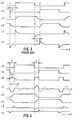
- FIG. 3 shows the essential signals of the known clock system of FIG. 1 in the time diagram.
- the voltage curves u1, u2 at the first and second load capacitors c1, c2 result from the two non-overlapping and antiphase clock signals t1, t2.
- the associated charging and discharging currents i1, i2 show which load capacity is being discharged or charged.
- the non-overlap area is essentially predetermined by the switching interval ti of the first and second clock t1, t2.
- the two clocks t3, t4 are also in phase opposition and not overlapping, with both clocks simultaneously being at zero potential in the switching interval ti.
- the functioning of the switched current path 5 assumes that there is a voltage difference between the first and second clock lines 9.1, 9.2, because otherwise no equalizing current i5 can flow.
- the gate signal t5 which is approximately identical in time to the switching interval ti, switches the current path 5 in the on state, so that the compensating current i5 can flow.
- the excited oscillation would subside through the damping elements in the resonance circuit, this is shown schematically in diagram i5 by the interrupted oscillation trains.
- the compensating current i5 remains at the zero value until a new gate pulse closes the resonance circuit again on the new edge change.
- the gate pulse in the gate signal t5 occurs at twice the frequency of the two clocks t1, t2.
- the resulting voltage curve u3, u4 on the two load capacitances c1, c2 shows that the overlap point is approximately half the edge voltage. This is still sufficient for safe operation in the high-speed range.
- the current pulses i3, i4, which are coupled to the driver stages 1, 2, are significantly smaller than the corresponding current pulses i1, i2 in FIG. 3 because part of the charging or discharging takes place through the compensating current i5.
- the equalizing current i5 generates only a very small interference field because the radiation area is limited to the monolithically integrated circuit and is therefore very small.
- the current pulses i3, i4, which over the Supply lines have to flow are reduced, so that the interference radiation has become smaller as desired.
Landscapes
- Electronic Switches (AREA)
- Manipulation Of Pulses (AREA)
Applications Claiming Priority (2)
| Application Number | Priority Date | Filing Date | Title |
|---|---|---|---|
| DE19548629A DE19548629C1 (de) | 1995-12-23 | 1995-12-23 | Komplementäres Taktsystem |
| DE19548629 | 1995-12-23 |
Publications (1)
| Publication Number | Publication Date |
|---|---|
| EP0780982A1 true EP0780982A1 (fr) | 1997-06-25 |
Family
ID=7781341
Family Applications (1)
| Application Number | Title | Priority Date | Filing Date |
|---|---|---|---|
| EP96120620A Withdrawn EP0780982A1 (fr) | 1995-12-23 | 1996-12-20 | Système d'horloge complémentaire |
Country Status (4)
| Country | Link |
|---|---|
| US (1) | US5736882A (fr) |
| EP (1) | EP0780982A1 (fr) |
| JP (1) | JPH09321591A (fr) |
| DE (1) | DE19548629C1 (fr) |
Families Citing this family (12)
| Publication number | Priority date | Publication date | Assignee | Title |
|---|---|---|---|---|
| US5852378A (en) * | 1997-02-11 | 1998-12-22 | Micron Technology, Inc. | Low-skew differential signal converter |
| US6104209A (en) | 1998-08-27 | 2000-08-15 | Micron Technology, Inc. | Low skew differential receiver with disable feature |
| US5877612A (en) * | 1997-03-24 | 1999-03-02 | The United States Of America As Represented By The Secretary Of The Navy | Amplification of signals from high impedance sources |
| DE19714980C2 (de) * | 1997-04-10 | 2001-01-04 | Asm Automation Sensorik Messte | Ultraschall-Positionssensor mit einem Impulsgenerator zur Erzeugung von kurzen Spannungsimpulsen |
| US6212482B1 (en) | 1998-03-06 | 2001-04-03 | Micron Technology, Inc. | Circuit and method for specifying performance parameters in integrated circuits |
| DE19821458C1 (de) * | 1998-05-13 | 1999-11-18 | Siemens Ag | Schaltungsanordnung zur Erzeugung komplementärer Signale |
| FR2829599A1 (fr) * | 2001-09-07 | 2003-03-14 | St Microelectronics Sa | Circuit de commande de bus |
| US6650163B1 (en) * | 2002-08-08 | 2003-11-18 | International Business Machines Corporation | Clock generator for integrated circuit |
| JP4097561B2 (ja) * | 2003-05-09 | 2008-06-11 | 富士通株式会社 | 遅延補償機能付き差動クロック生成回路 |
| US7633182B2 (en) | 2005-11-09 | 2009-12-15 | Bae Systems Advanced Technologies, Inc. | Bipolar pulse generators with voltage multiplication |
| WO2020039977A1 (fr) * | 2018-08-21 | 2020-02-27 | ソニーセミコンダクタソリューションズ株式会社 | Dispositif de circuit à semi-conducteur et système équipé d'un dispositif de circuit à semi-conducteur |
| CN110719091B (zh) * | 2019-10-31 | 2023-08-04 | 宁波飞芯电子科技有限公司 | 互补信号生成电路 |
Citations (7)
| Publication number | Priority date | Publication date | Assignee | Title |
|---|---|---|---|---|
| JPH02216910A (ja) * | 1989-02-17 | 1990-08-29 | Fujitsu Ltd | バッファ回路 |
| EP0395146A1 (fr) * | 1989-04-25 | 1990-10-31 | Koninklijke Philips Electronics N.V. | Circuit de commande pour au moins une électrode d'horloge d'un circuit intégré |
| US5311136A (en) * | 1991-11-28 | 1994-05-10 | Kabushiki Kaisha Toshiba | Gradient power source apparatus for magnetic resonance imaging system |
| WO1994015394A1 (fr) * | 1992-12-19 | 1994-07-07 | Geoffrey Philip Harvey | Cuircuit electronique a faible puissance comprenant un systeme a resonance et des circuits de fonctions |
| DE4430078A1 (de) * | 1994-08-25 | 1995-02-02 | Manfred Prof Dr Ing Gekeler | Schaltungsanordnung zur Vermeidung von Schaltverlusten eines Zweigpaares eines selbstgeführten Stromrichters mit eingeprägter Zwischenkreisgleichspannung |
| EP0680148A2 (fr) * | 1994-04-18 | 1995-11-02 | AT&T Corp. | Circuit d'horloge à faible consommation |
| US5508639A (en) * | 1995-01-13 | 1996-04-16 | Texas Instruments Incorporated | CMOS clock drivers with inductive coupling |
Family Cites Families (5)
| Publication number | Priority date | Publication date | Assignee | Title |
|---|---|---|---|---|
| DE2448117A1 (de) * | 1974-10-09 | 1976-04-22 | Merk Gmbh Telefonbau Fried | Schaltungsanordnung fuer einen mindestens zwei zueinander phasenverschobene taktfolgen gleicher frequenz liefernden taktgenerator |
| US3961269A (en) * | 1975-05-22 | 1976-06-01 | Teletype Corporation | Multiple phase clock generator |
| JPS59221113A (ja) * | 1983-05-31 | 1984-12-12 | Sony Corp | 2相信号発生回路 |
| DE58908782D1 (de) * | 1989-09-22 | 1995-01-26 | Itt Ind Gmbh Deutsche | Zweiphasentaktgenerator. |
| US5041738A (en) * | 1989-12-04 | 1991-08-20 | Advanced Micro Devices, Inc. | CMOS clock generator having an adjustable overlap voltage |
-
1995
- 1995-12-23 DE DE19548629A patent/DE19548629C1/de not_active Expired - Fee Related
-
1996
- 1996-12-09 US US08/762,133 patent/US5736882A/en not_active Expired - Fee Related
- 1996-12-20 EP EP96120620A patent/EP0780982A1/fr not_active Withdrawn
- 1996-12-24 JP JP8344166A patent/JPH09321591A/ja active Pending
Patent Citations (7)
| Publication number | Priority date | Publication date | Assignee | Title |
|---|---|---|---|---|
| JPH02216910A (ja) * | 1989-02-17 | 1990-08-29 | Fujitsu Ltd | バッファ回路 |
| EP0395146A1 (fr) * | 1989-04-25 | 1990-10-31 | Koninklijke Philips Electronics N.V. | Circuit de commande pour au moins une électrode d'horloge d'un circuit intégré |
| US5311136A (en) * | 1991-11-28 | 1994-05-10 | Kabushiki Kaisha Toshiba | Gradient power source apparatus for magnetic resonance imaging system |
| WO1994015394A1 (fr) * | 1992-12-19 | 1994-07-07 | Geoffrey Philip Harvey | Cuircuit electronique a faible puissance comprenant un systeme a resonance et des circuits de fonctions |
| EP0680148A2 (fr) * | 1994-04-18 | 1995-11-02 | AT&T Corp. | Circuit d'horloge à faible consommation |
| DE4430078A1 (de) * | 1994-08-25 | 1995-02-02 | Manfred Prof Dr Ing Gekeler | Schaltungsanordnung zur Vermeidung von Schaltverlusten eines Zweigpaares eines selbstgeführten Stromrichters mit eingeprägter Zwischenkreisgleichspannung |
| US5508639A (en) * | 1995-01-13 | 1996-04-16 | Texas Instruments Incorporated | CMOS clock drivers with inductive coupling |
Non-Patent Citations (1)
| Title |
|---|
| PATENT ABSTRACTS OF JAPAN vol. 014, no. 518 (E - 1001) 14 November 1990 (1990-11-14) * |
Also Published As
| Publication number | Publication date |
|---|---|
| JPH09321591A (ja) | 1997-12-12 |
| US5736882A (en) | 1998-04-07 |
| DE19548629C1 (de) | 1997-07-24 |
Similar Documents
| Publication | Publication Date | Title |
|---|---|---|
| DE2541131C2 (de) | Schaltungsanordnung zum Konstanthalten der Schaltverzögerung von FET-Inverterstufen in einer integrierten Schaltung | |
| EP0032737B1 (fr) | Circuit de filtre électrique utilisant au moins une inductance simulée, comprenant des commutateurs commandés, des condensateurs et des amplificateurs | |
| DE69700232T2 (de) | Ladungspumpe für eine Phasenregelschleife | |
| DE69522447T2 (de) | Puls-zähl-fm-demodulator und empfänger damit | |
| DE60030589T2 (de) | Verfahren zur steuerspannungsversorgung für varaktoren, zur verminderung des phasenrauschens in elektronischen oszillatoren | |
| DE69310308T2 (de) | Negative Hochleistungsladungspumpe | |
| DE19548629C1 (de) | Komplementäres Taktsystem | |
| DE2143093C2 (de) | Mehrphasenfeldeffekttransistor- Steuerungsschaltung | |
| DE3218535C2 (fr) | ||
| DE3050199T1 (de) | Dynamic ratioless circuitry for random logic applications | |
| DE102014220406A1 (de) | Treiberschaltung für eine Induktivität und aktive Sendeeinrichtung mit einer Treiberschaltung | |
| WO1991020129A1 (fr) | Circuit pour la limitation de la vitesse de montee des signaux de sortie de circuits integres | |
| DE3237778A1 (de) | Dynamisches schieberegister | |
| DE69121175T2 (de) | Flipflop-Schaltung mit einem CMOS-Hysterese-Inverter | |
| DE2623219B2 (de) | Verfahren zum Betreiben einer Leseverstärkerschaltung für einen dynamischen MOS-Speicher und Anordnung zur Durchführung dieses Verfahrens | |
| DE112017004675T5 (de) | RF-Schalter für kapazitive Oszillatorabstimmung | |
| DE69522498T2 (de) | Signalübertragungsverfahren, Signalübertragungsschaltkreis und dafür geeigneter integrierter Halbleiterschaltkreis | |
| DE68922506T2 (de) | Frequenzteilerschaltung. | |
| DE2604497C2 (de) | MOS-Oszillatorschaltung | |
| DE10345131B4 (de) | RC-Oszillatorschaltung | |
| DE102005042789B4 (de) | Schwingkreis und Oszillator mit Schwingkreis | |
| DE3853983T2 (de) | Elektronischer Oszillator. | |
| DE69323770T2 (de) | Elektronischer kleinleistungskreis mit einem resonanzsystem und einem funktionsschaltkreis | |
| DE4312050A1 (de) | Ausgangsschaltung mit offener Drain | |
| EP1033814B1 (fr) | Circuit intégré pour la génération de deux signaux d'horloge sans chevauchement |
Legal Events
| Date | Code | Title | Description |
|---|---|---|---|
| PUAI | Public reference made under article 153(3) epc to a published international application that has entered the european phase |
Free format text: ORIGINAL CODE: 0009012 |
|
| AK | Designated contracting states |
Kind code of ref document: A1 Designated state(s): DE FR NL |
|
| RAP1 | Party data changed (applicant data changed or rights of an application transferred) |
Owner name: MICRONAS INTERMETALL GMBH |
|
| 17P | Request for examination filed |
Effective date: 19971229 |
|
| STAA | Information on the status of an ep patent application or granted ep patent |
Free format text: STATUS: THE APPLICATION HAS BEEN WITHDRAWN |
|
| 18W | Application withdrawn |
Withdrawal date: 19980921 |