EP0782251A1 - Detektor mit selbsttätiger Regelung der Vorspannung einer PIN-Fotodiode - Google Patents
Detektor mit selbsttätiger Regelung der Vorspannung einer PIN-Fotodiode Download PDFInfo
- Publication number
- EP0782251A1 EP0782251A1 EP96402898A EP96402898A EP0782251A1 EP 0782251 A1 EP0782251 A1 EP 0782251A1 EP 96402898 A EP96402898 A EP 96402898A EP 96402898 A EP96402898 A EP 96402898A EP 0782251 A1 EP0782251 A1 EP 0782251A1
- Authority
- EP
- European Patent Office
- Prior art keywords
- photodiode
- pin
- cathode
- value
- anode
- Prior art date
- Legal status (The legal status is an assumption and is not a legal conclusion. Google has not performed a legal analysis and makes no representation as to the accuracy of the status listed.)
- Granted
Links
- 230000010287 polarization Effects 0.000 claims description 24
- 239000003990 capacitor Substances 0.000 claims description 11
- 238000001514 detection method Methods 0.000 claims description 5
- 230000003287 optical effect Effects 0.000 abstract description 20
- 230000035945 sensitivity Effects 0.000 description 9
- 239000013307 optical fiber Substances 0.000 description 6
- 230000007423 decrease Effects 0.000 description 5
- 230000008901 benefit Effects 0.000 description 2
- 238000006073 displacement reaction Methods 0.000 description 2
- 230000006798 recombination Effects 0.000 description 2
- 238000005215 recombination Methods 0.000 description 2
- 230000001052 transient effect Effects 0.000 description 2
- 240000008042 Zea mays Species 0.000 description 1
- 230000006978 adaptation Effects 0.000 description 1
- 230000003321 amplification Effects 0.000 description 1
- 230000015556 catabolic process Effects 0.000 description 1
- 230000003247 decreasing effect Effects 0.000 description 1
- 238000006731 degradation reaction Methods 0.000 description 1
- 230000000694 effects Effects 0.000 description 1
- 230000005684 electric field Effects 0.000 description 1
- 238000003199 nucleic acid amplification method Methods 0.000 description 1
- 238000005457 optimization Methods 0.000 description 1
- 229920006395 saturated elastomer Polymers 0.000 description 1
- 238000009738 saturating Methods 0.000 description 1
- 238000000926 separation method Methods 0.000 description 1
- 230000006641 stabilisation Effects 0.000 description 1
- 238000011105 stabilization Methods 0.000 description 1
Images

Classifications
-
- H—ELECTRICITY
- H03—ELECTRONIC CIRCUITRY
- H03F—AMPLIFIERS
- H03F3/00—Amplifiers with only discharge tubes or only semiconductor devices as amplifying elements
- H03F3/04—Amplifiers with only discharge tubes or only semiconductor devices as amplifying elements with semiconductor devices only
- H03F3/08—Amplifiers with only discharge tubes or only semiconductor devices as amplifying elements with semiconductor devices only controlled by light
- H03F3/087—Amplifiers with only discharge tubes or only semiconductor devices as amplifying elements with semiconductor devices only controlled by light with IC amplifier blocks
Definitions
- the invention lies in the field of devices for converting an optical quantity into an electrical quantity.
- a converter of an optical quantity, for example of optical energy, in an electrical quantity, for example a voltage or a current is a converter of an optical quantity, for example of optical energy, in an electrical quantity, for example a voltage or a current.
- This converter is a PIN photodiode.
- i (t) is the instantaneous intensity of the current
- S is the sensitivity of the PIN photodiode expressed in Amperes per Watt
- P (t) is the value of the instantaneous optical power received by the PIN photodiode.
- the incident optical powers being generally from low to very low value, it is the same for the value of the photodetected current and it is understandable that it is necessary to amplify the latter with extreme care.
- Such amplification quality is obtained by using a so-called transimpedance type preamplification stage obtained by wiring a resistor Rg between the output and the input e (-) of a gain amplifier Gv having rather exceptional characteristics: produces gain x band greater than several tens of GHz in multiple applications.
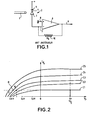
- FIG. 1 A known example of embodiment of such a photodetection stage is shown in FIG. 1.
- This figure represents an end 1 of an optical fiber transmitting a light wave modulated by a video frequency signal.
- the modulated light energy is received by a PIN photodiode 2 comprising an anode (P junction) 3, an intrinsic zone 4 and a cathode 5.
- the PIN photodiode 2 is in known manner reverse biased, that is to say that a positive voltage is applied to its cathode 5. Under these conditions, the PIN photodiode 2 delivers a current which flows from its cathode 5 to its anode 3. This current is proportional to the value of the incident optical power.
- the proportionality ratio represents the sensitivity of the PIN 2 photodiode.
- the curves representing the value of the photodetected current I ph as a function of the reverse bias voltage V p are represented in FIG. 2.
- Each of the curves C1 ... C5 in FIG. 2 is the curve representing the value of the photodetected current for a photoelectric power constant as a function of the bias voltage.
- V po the operating point of the PIN 2 photodiode will move on a vertical line shown in FIG. 2 by a dotted line passing through the value V in and parallel to the axis I ph representing the currents as a function of the powerful incident.
- the current I ph is amplified by a transimpedance preamplification stage 6 having a negative input 7, a positive input 8, an output 9 and a feedback resistance Rg 10 connected between the output 9 and the negative input 7.
- G is the gain of the transimpedance preamplification stage 6.
- V s (t) SP h (t) Rg can reach a very high value. Under these conditions, the transimpedance preamplification stage 6 becomes saturated and no longer functions linearly.
- This solution results in a degradation of the signal-to-noise ratio intrinsic to the optical receiver due to the increase in the term.
- ieff (Rg) ⁇ [Rg] 1/2 .
- ⁇ is a coefficient of proportionality
- a second known embodiment aiming to avoid saturation of the transimpedance preamplification stage 6 consists in inserting an attenuator in the optical link to prevent P (t) from exceeding the maximum admissible value P (t) maximum. This constraint optimization of each link is no longer accepted by users today.
- This embodiment obliges the latter to measure or calculate the average incident optical power to determine the value of the attenuator to be inserted.
- a third known solution consists in substituting an avalanche photodiode for the PIN 2 photodiode.
- the value of the multiplication factor M is a function of the value of the bias voltage of the avalanche photodiode.
- the present invention relates to a transimpedance preamplification stage using a detection PIN photodiode whose average output current remains lower than the current causing the saturation of the transimpedance preamplification stage, this without decreasing the value of the signal / noise ratio of this stage of transimpedance preamplification.
- the device according to the invention has a greater dynamic range of incident light power than the PIN photodiode devices according to the prior art.
- the device according to the invention has a greater dynamic range of light power reception than the PIN photodiode devices of the prior art.
- the device according to the invention can be used without any particular precautions or adjustments, at one end of an optical fiber, the other end of which receives light power from a transmitter, or from a repeater, this practically whatever or the distance between the transmitter or the repeater and the device according to the invention.
- the use of the PIN photodiode photodetector device according to the invention frees the user from any concern for adapting the device to the average level of the optical power received locally. Adaptation takes place automatically.
- the invention relates to a device for detecting a signal carried by a modulated light wave, the device receiving the wave on a PIN photodiode having two electrodes, an anode and a cathode, as well as a part intrinsic, at least one of the electrodes of the PIN photodiode being connected to biasing means, the PIN photodiode delivering when it is reverse biased by a positive voltage applied between its cathode and its anode, a photodetection current i ( t) proportional to the power of the incident light wave, detection device characterized in that the polarization means of the PIN photodiode are capable of applying to the PIN photodiode two polarization states, a first and a second, the polarization being established automatically in the first or in the second state as a function of the average light power received, in the first state corresponding to average light powers received less than one threshold value P h threshold, the photodiode is reverse biased by the biasing means;
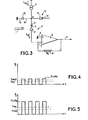
- a PIN photodiode 2 comprising an anode 3, an intrinsic zone 4 and a cathode 5, is supplied by a modulated light source, represented schematically in this embodiment by one end 1 of an optical fiber.
- the anode 3 of the photodiode 2 is connected to a negative input of a transimpedance preamplification stage 6.
- the positive input of this transimpedance preamplification stage 6 is in this example connected to ground.
- a feedback resistance Rg 10 is connected between the output 9 of the transimpedance preamplification stage 6 and the negative input 7.
- polarization means are connected for example at a point A to the cathode 5 of the PIN photodiode 2.
- these means comprise, connected to point A, a generator constant current 11, a capacitor 12 having two connections 13 and 14, one of which 14 is connected to point A, a diode 15 having a cathode 16 and an anode 17.
- the anode 17 of the diode 15 is connected to point A
- the constant current generator 11, the anode 17 of the diode 15 and a connection 14 of the capacitor 12 are connected at point A to the cathode 5 of the PIN photodiode 2.
- the means 11, 12 and 15 constitute, in this exemplary embodiment, the polarization means of the PIN 2 photodiode.
- FIGS. 4 and 5 are curves which each represent, as a function of time, a light power incident on the PIN 2 photodiode. These curves are constituted by a succession of zero and then positive powers alternately succeeding each other for equal periods.
- the positive level P h peak is such that the average power received is less than a threshold power P h threshold determined in a known manner from the saturation voltage of the transimpedance preamplification stage 6.
- This case which corresponds to the case where the emitting source is relatively far from the photodiode PIN 2, corresponds to the first state of polarization of the device according to the invention.
- the positive level P h peak is such that the average power received is greater than a power threshold P h threshold determined in known manner from the saturation voltage of the transimpedance preamplification stage 6.
- P h threshold determined in known manner from the saturation voltage of the transimpedance preamplification stage 6.
- the average light power which causes an output voltage saturating the transimpedance preamplification stage 6 is the same.
- the average power received is equal to half the peak value of the light power received.
- the average power received is shown by a dotted line, parallel to the time axis and located at level P my .
- the level P my has the value half of the level P h peak.
- the threshold level P h is also represented by a parallel to the time axis. In FIG. 4, the level P my is lower than the level P h threshold. It is the opposite in Figure 5.
- the constant current generator 11 delivers a preprogrammed current I my flowing from the constant current generator 11 to the point A.
- the current I my is such that a voltage across the resistor feedback Rg 10 having the value I my x Rg is less than the saturation voltage of the preamplification stage transimpedance 6.
- the voltage at point A remains equal to V in .
- the operating point of the PIN 2 photodiode is always defined by the polarization voltage V po . If momentarily as shown voluntarily in FIG. 4, the peak power P h of photodetection becomes greater than the threshold power P h threshold, this means that momentarily, the instantaneous current I ph is greater than I my . The difference I my - I ph becoming negative, this means that the capacity 12 will discharge. The value of the voltage at point A will drop and block the diode 15. If the period during which I ph is greater than I my is sufficiently short, the voltage drop will be slight and this will not affect the operation of the PIN photodiode 2, insofar as, as shown in FIG.
- the response of the photodiode PIN 2 that is to say the value of the current I ph is the same and only depends on the value of the light power received.
- the capacitor 12 When the photodetected power becomes lower than the threshold power P h threshold, the value of the current I my - I ph becomes positive again, the capacitor 12 will benefit from a charging current. The voltage at point A will increase until the diode 15 is conductive. Thus, when the average value of the photodetected current is stably lower than that of the current delivered by the constant current generator 11, the PIN photodiode 2 is polarized by stably in reverse. Photodetected currents momentarily greater than the current delivered by the constant current generator 11 do not affect the behavior of the PIN photodiode 2.
- the constant current generator 11 delivers the same current as in the previous case. This current only depends on the characteristics of the transimpedance preamplification stage 6.
- the capacitor 12 will discharge with a discharge current I ph - I my .
- the potential at A will drop, the diode 15 will be blocked.
- the recharging periods of the capacity 12 and the values of the recharging current corresponding to the periods where the photodetected power is less than the threshold power P h threshold will be insufficient to recharge the capacity 12.
- the photodetected current is on average greater than the current delivered by the constant current generator 11.
- the capacitor 12 will discharge regularly and even charge so that the voltage at point A will become negative .
- the PIN 2 photodiode will be directly polarized.
- the value of the photodetected current delivered by the photodiode PIN 2 when it is forward biased is represented on the left part of FIG. 2.
- the abscissa scale is on this left part greater than that of the right part so as to better make the curves C1 to C5 perceptible.
- the photodiode PIN 2 is polarized directly.
- the average value of the photodetected current stabilizes at the programmed value I my .
- Such stabilization is due to the following phenomenon: due to the voltage drop between anode 3 and cathode 5 of the PIN photodiode 2, the electric field in the intrinsic zone 4 of the PIN 2 photodiode becomes weak and insufficient to ensure a good separation of pairs positive electron-holes. There is therefore a certain recombination of the positive electron-hole pairs released in the intrinsic zone 4 under the effect of the incident photons.
- a state of equilibrium is established between the value of the forward bias voltage resulting from the discharge of the capacitor 12 and the percentage of recombination of the positive electron-hole pairs.
- the equilibrium state is such that the average value of the photodetected current is established at the value of the current I my delivered by the constant current generator 11. This operating point moves on a straight line parallel to the abscissa axis . This line is shown on the left side of Figure 2.
- the operating point of the PIN 2 photodiode is moved automatically.
- the photodiode PIN 2 is reverse biased and operates in the known manner.
- the photodiode PIN 2 is forward biased. The reverse or direct polarization is established automatically according to the average incident power.
- the solution according to the invention gives - beyond a certain incident optical power P h threshold - to the PIN 2 photodiode a sensitivity inversely proportional to the value of the incident optical power P.
- P h threshold - the incident optical power
- the polarization means described in relation to FIG. 3 have the advantage of simplicity. A person skilled in the art can however easily find other means of moving the operating point as a function of the average incident power received by the PIN 2 photodiode.
- FIG. 6 This figure represents the same elements as those of FIG. 3 but in the case of FIG. 6, the polarization means of the PIN photodiode 2 are connected at a point E connected to the anode 3 of the PIN photodiode 2. In this connection mode, it is the cathode 16 of the biasing diode 15 which is connected to point E.
- the current generated by the constant current generator 11 is in this case directed from point E to the constant current generator 11. The operation is the same as in the previous case.
- the biasing diode 15 could be replaced by a transistor having its base connected to the point E.
Landscapes
- Engineering & Computer Science (AREA)
- Power Engineering (AREA)
- Optical Communication System (AREA)
- Amplifiers (AREA)
- Manipulation Of Pulses (AREA)
- Electronic Switches (AREA)
Applications Claiming Priority (2)
| Application Number | Priority Date | Filing Date | Title |
|---|---|---|---|
| FR9515744 | 1995-12-29 | ||
| FR9515744A FR2743224B1 (fr) | 1995-12-29 | 1995-12-29 | Dispositif de detection comportant des moyens d'asservissement automatique de la sensibilite d'une photodiode pin |
Publications (2)
| Publication Number | Publication Date |
|---|---|
| EP0782251A1 true EP0782251A1 (de) | 1997-07-02 |
| EP0782251B1 EP0782251B1 (de) | 2001-10-24 |
Family
ID=9486152
Family Applications (1)
| Application Number | Title | Priority Date | Filing Date |
|---|---|---|---|
| EP96402898A Expired - Lifetime EP0782251B1 (de) | 1995-12-29 | 1996-12-26 | Detektor mit selbsttätiger Regelung der Vorspannung einer PIN-Fotodiode |
Country Status (5)
| Country | Link |
|---|---|
| US (1) | US5889605A (de) |
| EP (1) | EP0782251B1 (de) |
| JP (1) | JP3863613B2 (de) |
| DE (1) | DE69616255T2 (de) |
| FR (1) | FR2743224B1 (de) |
Cited By (2)
| Publication number | Priority date | Publication date | Assignee | Title |
|---|---|---|---|---|
| EP0927888A1 (de) * | 1997-12-29 | 1999-07-07 | Deutsche Thomson Brandt | Photodiodendetektorschaltung zur automatischen Anpassung an Vorwärtsvorspannung oder umgekehrter Vorspannung |
| EP0928971A1 (de) * | 1997-12-29 | 1999-07-14 | Deutsche Thomson Brandt | Photodiodendetektorschaltung zur automatischen Anpassung an Vorwärtsvorspannung oder umgekehrter Vorspannung |
Families Citing this family (10)
| Publication number | Priority date | Publication date | Assignee | Title |
|---|---|---|---|---|
| US6166840A (en) * | 1996-04-29 | 2000-12-26 | Esel-Krabbe Systems A/S | Electronic circuit for receiving and discriminating modulated light and an electronic price display comprising said circuit |
| JP3583704B2 (ja) * | 2000-01-12 | 2004-11-04 | 独立行政法人 科学技術振興機構 | 温度測定装置、熱型赤外線イメージセンサ及び温度測定方法 |
| US7068951B2 (en) * | 2002-04-11 | 2006-06-27 | Optical Communication Products, Inc. | Optical signal receiver with RPM, data and data bar output |
| CN100524381C (zh) * | 2003-01-14 | 2009-08-05 | 皇家飞利浦电子股份有限公司 | 用于具有光电二极管的遥控接收机的电路装置和方法 |
| DE102005002195A1 (de) * | 2005-01-17 | 2006-07-27 | Siemens Ag | Verfahren und Anordnung zur Regeneration eines optischen Datensignals |
| US8130298B2 (en) * | 2008-02-07 | 2012-03-06 | International Business Machines Corporation | Wide dynamic range image sensor utilizing switch current source at pre-determined switch voltage per pixel |
| JP5682152B2 (ja) * | 2010-06-18 | 2015-03-11 | ソニー株式会社 | 光受信機および光伝送システム |
| US11005573B2 (en) * | 2018-11-20 | 2021-05-11 | Macom Technology Solutions Holdings, Inc. | Optic signal receiver with dynamic control |
| US12013423B2 (en) | 2020-09-30 | 2024-06-18 | Macom Technology Solutions Holdings, Inc. | TIA bandwidth testing system and method |
| US11658630B2 (en) | 2020-12-04 | 2023-05-23 | Macom Technology Solutions Holdings, Inc. | Single servo loop controlling an automatic gain control and current sourcing mechanism |
Citations (8)
| Publication number | Priority date | Publication date | Assignee | Title |
|---|---|---|---|---|
| DE2841940A1 (de) * | 1978-09-27 | 1980-04-10 | Bosch Gmbh Robert | Schutzschaltung fuer einen photodioden-vorverstaerker |
| FR2527027A1 (fr) * | 1982-05-15 | 1983-11-18 | Kabelmetal Electro Gmbh | Dispositif de circuit pour un convertisseur optique/electrique |
| GB2135551A (en) * | 1983-02-11 | 1984-08-30 | British Telecomm | Optical receivers |
| JPS59230307A (ja) * | 1983-06-14 | 1984-12-24 | Matsushita Electric Ind Co Ltd | 光受信装置 |
| GB2181832A (en) * | 1985-10-19 | 1987-04-29 | Plessey Co Plc | Improvements relating to optical detecting arrangements |
| DE3543677A1 (de) * | 1985-12-11 | 1987-06-19 | Standard Elektrik Lorenz Ag | Vorverstaerker hoher dynamik und empfindlichkeit |
| GB2194406A (en) * | 1986-07-18 | 1988-03-02 | Gen Electric Plc | Optical signal receiver circuits |
| EP0402044A2 (de) * | 1989-06-09 | 1990-12-12 | Nortel Networks Corporation | Optische Empfänger |
Family Cites Families (2)
| Publication number | Priority date | Publication date | Assignee | Title |
|---|---|---|---|---|
| US5410282A (en) * | 1994-03-14 | 1995-04-25 | Tektronix, Inc. | Wide dynamic range amplifier with error correction |
| US5734300A (en) * | 1996-05-17 | 1998-03-31 | Lucent Technologies, Inc. | Optical receiver preamplifier dynamic range enhancing circuit and method |
-
1995
- 1995-12-29 FR FR9515744A patent/FR2743224B1/fr not_active Expired - Fee Related
-
1996
- 1996-12-26 EP EP96402898A patent/EP0782251B1/de not_active Expired - Lifetime
- 1996-12-26 DE DE69616255T patent/DE69616255T2/de not_active Expired - Lifetime
- 1996-12-27 US US08/773,908 patent/US5889605A/en not_active Expired - Lifetime
- 1996-12-27 JP JP35159396A patent/JP3863613B2/ja not_active Expired - Fee Related
Patent Citations (8)
| Publication number | Priority date | Publication date | Assignee | Title |
|---|---|---|---|---|
| DE2841940A1 (de) * | 1978-09-27 | 1980-04-10 | Bosch Gmbh Robert | Schutzschaltung fuer einen photodioden-vorverstaerker |
| FR2527027A1 (fr) * | 1982-05-15 | 1983-11-18 | Kabelmetal Electro Gmbh | Dispositif de circuit pour un convertisseur optique/electrique |
| GB2135551A (en) * | 1983-02-11 | 1984-08-30 | British Telecomm | Optical receivers |
| JPS59230307A (ja) * | 1983-06-14 | 1984-12-24 | Matsushita Electric Ind Co Ltd | 光受信装置 |
| GB2181832A (en) * | 1985-10-19 | 1987-04-29 | Plessey Co Plc | Improvements relating to optical detecting arrangements |
| DE3543677A1 (de) * | 1985-12-11 | 1987-06-19 | Standard Elektrik Lorenz Ag | Vorverstaerker hoher dynamik und empfindlichkeit |
| GB2194406A (en) * | 1986-07-18 | 1988-03-02 | Gen Electric Plc | Optical signal receiver circuits |
| EP0402044A2 (de) * | 1989-06-09 | 1990-12-12 | Nortel Networks Corporation | Optische Empfänger |
Non-Patent Citations (2)
| Title |
|---|
| GRAEME J: "CIRCUIT OPTIONS BOOST PHOTODIODE BANDWIDTH", EDN ELECTRICAL DESIGN NEWS, vol. 37, no. 11, 21 May 1992 (1992-05-21), pages 155 - 160, 162, XP000305515 * |
| PATENT ABSTRACTS OF JAPAN vol. 9, no. 106 (E - 313)<1829> 10 May 1985 (1985-05-10) * |
Cited By (4)
| Publication number | Priority date | Publication date | Assignee | Title |
|---|---|---|---|---|
| EP0927888A1 (de) * | 1997-12-29 | 1999-07-07 | Deutsche Thomson Brandt | Photodiodendetektorschaltung zur automatischen Anpassung an Vorwärtsvorspannung oder umgekehrter Vorspannung |
| EP0928971A1 (de) * | 1997-12-29 | 1999-07-14 | Deutsche Thomson Brandt | Photodiodendetektorschaltung zur automatischen Anpassung an Vorwärtsvorspannung oder umgekehrter Vorspannung |
| US6363044B1 (en) | 1997-12-29 | 2002-03-26 | Deutsche Thomson-Brandt Gmbh | Automatically adapting forward or reversed biased photodiode detection circuit |
| CN1109898C (zh) * | 1997-12-29 | 2003-05-28 | 德国汤姆逊-布朗特公司 | 自动自适应光电二极管偏压检测以及光强监控电路和方法 |
Also Published As
| Publication number | Publication date |
|---|---|
| DE69616255T2 (de) | 2002-07-04 |
| EP0782251B1 (de) | 2001-10-24 |
| DE69616255D1 (de) | 2001-11-29 |
| JP3863613B2 (ja) | 2006-12-27 |
| US5889605A (en) | 1999-03-30 |
| FR2743224B1 (fr) | 1998-03-06 |
| JPH1075214A (ja) | 1998-03-17 |
| FR2743224A1 (fr) | 1997-07-04 |
Similar Documents
| Publication | Publication Date | Title |
|---|---|---|
| EP0782251B1 (de) | Detektor mit selbsttätiger Regelung der Vorspannung einer PIN-Fotodiode | |
| EP0034957B1 (de) | Vorrichtung zur automatischen Regulierung der Ausgangsleistung eines Sendermoduls für ein Übertragungssystem mit optischen Fasern | |
| EP0817408B1 (de) | Empfänger für Übertragungssystem eines optischen Digitalsignals | |
| FR2634293A2 (fr) | Systeme de regulation du point de fonctionnement d'une alimentation a courant continu en zone de caracteristique generateur de tension ou de courant imposee | |
| FR2682227A1 (fr) | Circuit et procede de commande de retour de laser. | |
| FR2523782A1 (fr) | Circuit amplificateur a transistor a effet de champ | |
| EP0034082B1 (de) | Vorrichtung zur Alarmauslösung im Falle eines ungenügenden Übertragungspegels für den Empfängermodul eines Übertragungssystems mit optischen Fasern | |
| EP0176448A2 (de) | Vorrichtung zum Nachweis eines Lichtbündels, unter Verwendung einer Photodiode, mit einer Schaltung zur Einstellung des Arbeitspunktes | |
| EP0632585A1 (de) | Vorrichtung zur Steuerung der Vorspannung eines Verstärkers | |
| EP0586285B1 (de) | Optischer Sender-Empfänger für optische Datenübertragung und Schalteinrichtung | |
| FR2473234A1 (fr) | Circuit a impedance electriquement variable et a compensation par reaction | |
| EP0271938B1 (de) | Automatische Verstärkungsregelung einer Verstärkerschaltung | |
| EP0106728B1 (de) | Verfahren und Vorrichtung zur Verstärkungsstabilisierung eines fotoempfindlichen Avalanche-Bauelements | |
| FR2473232A1 (fr) | Amplificateur de puissance efficace a tensions d'alimentation decalees | |
| EP0692907B1 (de) | Schaltung zur Unterdrückung des Dunkelstromes eines Photodetektors | |
| EP0415503B1 (de) | Integrierte Schaltung mit einer Feststellung des Sättigungszustandes | |
| FR2520174A1 (fr) | Systeme de transmission de signaux numeriques sur fibre optique | |
| EP0141715A2 (de) | Vorrichtung zur automatischen Vorkorrektur von Nichtlinearitäten in einer Leistungsverstärkerkette, sowie ihre Anwendung in einem Fernsehsender | |
| EP0913961B1 (de) | Optischer Sender zur Rauschimpulsverringerung in einer faseroptischen Verbindung | |
| EP0560659B1 (de) | Verfahren und Vorrichtung zur optischen Übertragung eines Multiplexsignals mit elektrischen Trägern | |
| FR2711792A1 (fr) | Dispositif de mesure de flux lumineux. | |
| EP0847193A1 (de) | Zwischenfrequenzverstärker für Funkwellenempfänger | |
| FR2721715A1 (fr) | Dispositif de mesure de l'état de charge d'un générateur électrochimique. | |
| EP0961422B1 (de) | Optischer Sender mit mehreren optischen Quellen | |
| EP0532400A1 (de) | Diskriminator mit einer reduzierten Frequenzcharakteristik |
Legal Events
| Date | Code | Title | Description |
|---|---|---|---|
| PUAI | Public reference made under article 153(3) epc to a published international application that has entered the european phase |
Free format text: ORIGINAL CODE: 0009012 |
|
| AK | Designated contracting states |
Kind code of ref document: A1 Designated state(s): DE FR GB |
|
| 17P | Request for examination filed |
Effective date: 19970728 |
|
| GRAG | Despatch of communication of intention to grant |
Free format text: ORIGINAL CODE: EPIDOS AGRA |
|
| 17Q | First examination report despatched |
Effective date: 20001020 |
|
| GRAG | Despatch of communication of intention to grant |
Free format text: ORIGINAL CODE: EPIDOS AGRA |
|
| GRAH | Despatch of communication of intention to grant a patent |
Free format text: ORIGINAL CODE: EPIDOS IGRA |
|
| GRAH | Despatch of communication of intention to grant a patent |
Free format text: ORIGINAL CODE: EPIDOS IGRA |
|
| GRAA | (expected) grant |
Free format text: ORIGINAL CODE: 0009210 |
|
| AK | Designated contracting states |
Kind code of ref document: B1 Designated state(s): DE FR GB |
|
| REF | Corresponds to: |
Ref document number: 69616255 Country of ref document: DE Date of ref document: 20011129 |
|
| REG | Reference to a national code |
Ref country code: GB Ref legal event code: IF02 |
|
| GBT | Gb: translation of ep patent filed (gb section 77(6)(a)/1977) |
Effective date: 20020110 |
|
| PLBE | No opposition filed within time limit |
Free format text: ORIGINAL CODE: 0009261 |
|
| STAA | Information on the status of an ep patent application or granted ep patent |
Free format text: STATUS: NO OPPOSITION FILED WITHIN TIME LIMIT |
|
| 26N | No opposition filed | ||
| REG | Reference to a national code |
Ref country code: DE Ref legal event code: R081 Ref document number: 69616255 Country of ref document: DE Owner name: THOMSON LICENSING, FR Free format text: FORMER OWNER: THOMSON BROADCAST SYSTEMS, CERGY PONTOISE, FR Effective date: 20110217 |
|
| PGFP | Annual fee paid to national office [announced via postgrant information from national office to epo] |
Ref country code: GB Payment date: 20141230 Year of fee payment: 19 |
|
| PGFP | Annual fee paid to national office [announced via postgrant information from national office to epo] |
Ref country code: DE Payment date: 20141230 Year of fee payment: 19 |
|
| PGFP | Annual fee paid to national office [announced via postgrant information from national office to epo] |
Ref country code: FR Payment date: 20141230 Year of fee payment: 19 |
|
| REG | Reference to a national code |
Ref country code: DE Ref legal event code: R119 Ref document number: 69616255 Country of ref document: DE |
|
| GBPC | Gb: european patent ceased through non-payment of renewal fee |
Effective date: 20151226 |
|
| REG | Reference to a national code |
Ref country code: FR Ref legal event code: ST Effective date: 20160831 |
|
| PG25 | Lapsed in a contracting state [announced via postgrant information from national office to epo] |
Ref country code: DE Free format text: LAPSE BECAUSE OF NON-PAYMENT OF DUE FEES Effective date: 20160701 Ref country code: GB Free format text: LAPSE BECAUSE OF NON-PAYMENT OF DUE FEES Effective date: 20151226 |
|
| PG25 | Lapsed in a contracting state [announced via postgrant information from national office to epo] |
Ref country code: FR Free format text: LAPSE BECAUSE OF NON-PAYMENT OF DUE FEES Effective date: 20151231 |