EP0782260A2 - Entzerrer Filter Konfiguration für Realwert -und Komplexwertmusterbearbeitung - Google Patents
Entzerrer Filter Konfiguration für Realwert -und Komplexwertmusterbearbeitung Download PDFInfo
- Publication number
- EP0782260A2 EP0782260A2 EP96309561A EP96309561A EP0782260A2 EP 0782260 A2 EP0782260 A2 EP 0782260A2 EP 96309561 A EP96309561 A EP 96309561A EP 96309561 A EP96309561 A EP 96309561A EP 0782260 A2 EP0782260 A2 EP 0782260A2
- Authority
- EP
- European Patent Office
- Prior art keywords
- valued
- multiply
- signal
- equalizer filter
- signal samples
- Prior art date
- Legal status (The legal status is an assumption and is not a legal conclusion. Google has not performed a legal analysis and makes no representation as to the accuracy of the status listed.)
- Withdrawn
Links
- 238000000034 method Methods 0.000 claims abstract description 24
- 230000003111 delayed effect Effects 0.000 claims abstract description 10
- 230000003044 adaptive effect Effects 0.000 description 7
- 238000010586 diagram Methods 0.000 description 7
- 230000014509 gene expression Effects 0.000 description 4
- 238000006243 chemical reaction Methods 0.000 description 2
- 230000000295 complement effect Effects 0.000 description 2
- 238000012986 modification Methods 0.000 description 2
- 230000004048 modification Effects 0.000 description 2
- 230000008520 organization Effects 0.000 description 1
- 238000005070 sampling Methods 0.000 description 1
- 238000006467 substitution reaction Methods 0.000 description 1
- 230000001360 synchronised effect Effects 0.000 description 1
Images


Classifications
-
- H—ELECTRICITY
- H03—ELECTRONIC CIRCUITRY
- H03H—IMPEDANCE NETWORKS, e.g. RESONANT CIRCUITS; RESONATORS
- H03H21/00—Adaptive networks
- H03H21/0012—Digital adaptive filters
-
- H—ELECTRICITY
- H03—ELECTRONIC CIRCUITRY
- H03H—IMPEDANCE NETWORKS, e.g. RESONANT CIRCUITS; RESONATORS
- H03H2218/00—Indexing scheme relating to details of digital filters
- H03H2218/04—In-phase and quadrature [I/Q] signals
Definitions
- the invention relates to digital signal filter architectures and, more particularly, to equalizer filter architectures or configurations.
- Equalizer filters and particularly adaptive equalizer filters, are well-known and used in a variety of applications. See, for example, Adaptive Filter Theory, by S. Haykin, available from Prentice-Hall, Inc., Englewood Cliffs, NJ, 1992, herein incorporated by reference.
- equalizer filters or equalizer filter configurations may be employed to reduce intersymbol interference (ISI) that may appear as ghosts in a received video signal, for example.
- ISI intersymbol interference
- An equalizer filter or equalizer filter configuration having the capability to take advantage of this trade-off may be desirable.
- an equalizer filter configuration comprises: a plurality of memory blocks; and a plurality of filter blocks.
- the respective pluralities of memory blocks and filter blocks are coupled so that the equalizer filter configuration has the capability to process input signal samples, the input signal samples comprising signal samples selected from the group consisting essentially of complex-valued signal samples and real-valued signal samples.
- a method of implementing an equalizer filter for processing complex-valued signal samples at a substantially predetermined signal sample rate comprises the steps of: providing current and selectively delayed real-valued and imaginary-valued signal sample components to the respective multipliers of two multiply-accumulate units; applying selected complex-valued coefficient signal components to the respective multipliers; and operating the two multiply-accumulate units so as to implement a predetermined number of taps of the equalizer filter in which a first unit of the two multiply-accumulate units produces a real-valued output signal and a second unit of the two multiply-accumulate units produces an imaginary-valued output signal.
- FIG. 3 is a block diagram illustrating an implementation 300 of a random access memory-based (RAM-based) architecture for an equalizer filter or equalizer filter configuration.
- discrete signal samples designated X(n) become available periodically.
- the discrete signal samples may be obtained by downconverting a radio frequency (RF) signal to produce an analog signal and then performing analog-to-digital (A/D) conversion at a substantially predetermined signal sample rate.
- RF radio frequency
- A/D analog-to-digital
- the digital signal samples comprise a predetermined number of binary digital signals, such as 10 bits, for example, provided in a parallel, twos complement format, for example.
- a plurality of real-valued digital signal samples may be provided, such as for vestigial sideband modulation (VSB).
- VSB vestigial sideband modulation
- each MAC unit may implement four equalizer filter taps because the clock frequency of the MAC unit is four times faster than the signal sample rate in this particular implementation.
- RAMs 310, 320, 311, and 321 each include two memory locations. As each discrete signal sample arrives at the 10 MHz rate, that signal sample may be written to a memory location in one of the RAMs and, likewise, the signal sample stored in that memory location may then be provided to MUX 330 and ultimately to filter blocks 365 and 375.
- currently available signal samples designated X(n)
- X(n) may be provided via MUX 330 and delayed signal samples designated, for example, as X(n-2), X(n-4), and X(n-6), may also be provided via MUX 330.
- 365OS(n) the Filter Block 365 output signal at sample period n.
- MAC units operating at 40 MHz, may each form four products in that time, as illustrated by expressions (1) above.
- signal sample X(n) is provided to multiplier 350.
- coefficients stored as signals in RAM 355, such as C 1 , C 3 , C 5 and C 7 are provided to multiplier 350 via MUX 325.
- the output signal of multiplier 350 is then provided to adder 390.
- the sum of the signal provided by multiplier 350 and the signal provided via MUX 305 is then provided by adder 390 to delay unit 360.
- MUX 305 provides a zero signal, as illustrated in FIG. 3. Therefore, the signal value provided to delay unit 360 is the product, C 1 X(n).
- MUX 330 may then provide a delayed signal sample, such as X(n-2) from RAM 321, for example. Again, this is provided to multiplier 350.
- RAM 355 then provides a signal for a coefficient, such as C 3, via MUX 325 to multiplier 350.
- the product, C 3 X(n-2), for example, is then produced by multiplier 350 and provided as a signal to adder 390.
- delay unit 360 then provides the previous product, stored as a signal, to MUX 305 so that it may be summed by adder 390 with the signal just produced by multiplier 350.
- the partial sum, C 1 X(n) + C 3 X(n-2), for example, is then provided to delay unit 360. This process is continued to obtain the expression for the output signal of filter block 365 provided in (1). Likewise, this partial sum is provided as the output signal of filter block 365 to the MAC unit of filter block 375 via port 362.
- the MAC unit of filter block 375 also receives input signal samples X(n), X(n-2), X(n-4), and X(n-6).
- the MAC unit of filter block 365 is also computing a partial sum.
- RAM 345 in this implementation stores different coefficient signals, such as for C 0 , C 2 , C 4 , and C 6 , for example.
- the partial sum computed by block 365 is then provided to filter block 375 via MUX 315. This is consistent with expressions (1).
- the output signal provided by the MAC unit of filter block 375 is also the equalizer filter output signal, Y(n). This may be summarized in accordance with the following equation.
- RAMs 355 and 345 store as signals the coefficients for the equalizer filter. Alternately, these RAMS may be updated with signals providing updated coefficients so that an adaptive equalizer may be implemented. Typically, updating of the coefficients is performed "off-line" and is based, at least in part, on an error signal or error signal samples produced by comparing the output signal of the adaptive equalizer with the output signal of a slicer.
- an equalizer filter in accordance with the invention is not restricted in scope in this respect.
- an update block may be employed, such as described in aforementioned concurrently filed Patent Application Serial No. (Raghunath 1) or Serial No. (Raghunath 2), although, again, the invention is not restricted in scope in this respect.
- equalizer filter shown will only process real-valued input signal samples.
- an equalizer filter had the capability to process either real-valued or complex-valued signal samples, depending upon the signal samples applied to the equalizer filter.
- QAM quadrature amplitude modulation
- VSB vestigial sideband modulation
- the former type of modulation produces complex-valued signal samples, whereas the latter type produces real-valued signal samples.
- the difficulty is that each approach typically employs a different equalizer filter configuration or architecture.
- a filter architecture having the capability to perform both types of signal processing without introducing a significant amount of additional hardware complexity or overhead would be desirable.
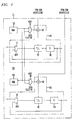
- FIG. 1 is a block diagram of a portion of an embodiment 100 of an equalizer filter or equalizer filter configuration in accordance with the invention.
- Embodiment 100 is illustrated as embodied on an integrated circuit (IC), although the invention is not restricted in scope in this respect.
- An embodiment of a RAM architecture that may be employed with this portion is illustrated in FIG. 2.
- Embodiment 100, shown in FIG. 1 has an architecture that allows the equalizer filter to process both real-valued signal samples and complex-valued signal samples, as described in more detail hereinafter. Assume in this particular embodiment that the complex-valued signal samples arrive at a 5 MHz rate, although the invention is not limited in scope in this respect.
- this signal sample rate provides an equivalent bit rate to the bit rate of the equalizer filter of FIG. 3, even though the signal sample rate is half of the signal sample rate for the filter configuration shown in FIG. 3.
- this particular embodiment of a filter block includes two MAC units, 140 and 150, whereas for the implementation shown in FIG. 3, a single MAC unit is employed for each filter block.
- embodiment 100 shown in FIG. 1 may be employed to operate like the implementation shown in FIG. 3 based upon the use of MUXes 30 and 40 in FIG. 1.
- MUXes 30 and 40 include a data selector that may be employed to select RAM 120 for MUX 30 and RAM 130 for MUX 40 so that MAC units 140 and 150 may each correspond to respective filter blocks of an equalizer filter for processing real-valued signal samples, such as filter block 365 and filter block 375 shown in FIG. 3, for example.
- the embodiment shown in FIG. 1 also has the additional capability to perform processing for complex-valued signal samples, which the embodiment shown in FIG. 3 does not have the capability to perform.
- MAC unit 140 provides a real-valued output signal sample whereas MAC unit 150 provides an imaginary-valued output signal sample.
- embodiment 100 comprises a filter block including two mutually-coupled MAC units.
- Each of the two mutually-coupled MAC units includes a MUX that mutually couples the MAC units so that the MAC units include the capability to share multiplier or coefficient signals stored in the RAMs of the two respective MAC units.
- the invention is not limited in scope in this respect.
- an equalizer filter in accordance with the invention to have the capability to process complex-valued signal samples, it should have the ability to process signal samples and coefficient signals in accordance with the following form.
- X(n) are the input signal samples
- Y(n) are the output signal samples
- C k are the coefficient signals.
- Y r (n), X r (n) and C rk represent real-valued components
- Y i (n), X i (n), and C ik represent imaginary-valued components of the respective signal samples and signals.
- a fractionally spaced linear equalizer (FSLE) is employed, although the invention is not limited in scope in this respect.
- N is 4 complex taps, in comparison with the 8 real taps for the implementation of FIG. 3.
- the output signal samples, Y(n) may be expressed in real-valued and imaginary-valued components in accordance with the following equations. Therefore, the real-valued and imaginary-valued components for the output signal samples of a filter block of an equalizer filter capable of processing complex-valued signal samples may have the following form.
- RTAP 100 is the output signal sample produced by MAC unit 140
- ITAP100 is the output signal sample produced by MAC unit 150 in this particular example.
- FIG. 1 merely illustrates an architecture in accordance with the invention for implementing a complex four tap equalizer filter.
- the invention is not limited in scope to MAC units having the precise structure of MAC units 140 and 150.
- Other embodiments of an MAC unit may provide satisfactory performance.
- embodiment 100 of an equalizer filter configuration in accordance with the invention is flexible and includes the capability to process both real-valued and complex-valued signal samples.
- this architecture may be extended in a variety of ways including: number of RAMs, clock frequency, signal sample rate, number of filter taps, number of filter blocks, and number of MAC units, to name only a few possible variations.
- the previous embodiment implements a 4 tap complex T/2 filter. Nonetheless, it may be extended to any size filter, including multiples of four, as illustrated.
- a 64-tap complex filter may employ 4 RAMs, each of size 32, and 16 complex filter blocks.
- complex-valued signal samples that are provided to MUX 230 are written to RAMs 210, 220, 215, and 225.
- the signal samples stored in the respective RAMs are then provided to MUX 240 for the filter blocks, such as embodiment 100 illustrated in FIG. 1.
- the signal sample rate for the complex-valued signal samples is half of the rate for the implementation illustrated in FIG. 3, although the signal samples are fractionally-spaced, sufficient time is provided to read and write the real-valued and imaginary-valued components of the signal samples.
- eight multiply operations may be performed in this particular embodiment, for example.
- the complex-valued signal sample may be made available, via MUX 230 and MUX 240, to embodiment 100, illustrated in FIG. 1.
- a signal sample component such as a real-valued component, X r (n-0.5), for example, may be provided via MUX 240 to multipliers 50 and 60 and then on the next clock cycle of the MAC units, which is eight times the signal sample rate
- another signal sample component such as the imaginary-valued component, X i (n-0.5), for example, may be provided via MUX 240 to multipliers 50 and 60.
- the real-valued and imaginary-valued signal component of this complex-valued signal sample may then be written into the RAMs and the real and imaginary-valued signal components of a signal sample stored in a selected memory location may then be read from the RAMs and provided by MUX 240, again to embodiment 100 illustrated in FIG. 1.
- These signal components have been effectively delayed by storage in the RAM. For example, signal components for X r (n-1.5) and X i (n-1.5), as illustrated in FIG. 4, may be read from the RAMs.
- the real-valued component, X r (n-1.5), for example, may be provided to multipliers 50 and 60, and, on yet another clock cycle, the imaginary-valued component, X i (n-1.5), for example, may be provided.
- This process may then be repeated for signal sample components X r (n), X i (n), X r (n-1), and X i (n-1).
- components X r (n) and X i (n) become available via MUXes 230 and 240, are stored in the RAMs, and then components X r (n-1) and X i (n-1) are read from the RAMs.
- FIG. 5 illustrates the signal sample components provided via MUX 240 to multipliers 50 and 60 during eight clock cycles synchronized with a single signal sample period for this particular embodiment.
- FIG. 4 illustrates a possible memory map of RAMs 210, 220, 215 and 225 for the delayed signal sample components.
- RAM 120 and RAM 130 respectively contain the real-valued and imaginary-valued components of the complex-valued coefficient signals that may be provided via MUXes 30 and 40 to multipliers 50 and 60 to ensure that the proper product-signal is formed by multipliers 50 and 60.
- FIG. 5 illustrates the signal sample components provided via MUX 240 to multipliers 50 and 60 during eight clock cycles synchronized with a single signal sample period for this particular embodiment.
- FIG. 4 illustrates a possible memory map of RAMs 210, 220, 215 and 225 for the delayed signal sample components.
- RAM 120 and RAM 130 respectively contain the real-valued and imaginary-valued components of the complex-valued coefficient signals that may be provided via MUXes 30
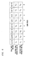
- FIG. 6 is a table illustrating the real-valued and imaginary-valued coefficient signals to be provided via MUXes 30 and 40 for processing with the various real-valued and imaginary-valued signal components provided via MUX 240.
- the top row corresponds to the signal sample components shown in FIG. 5 and the next two rows provide the coefficient signal components provided by the designated MUX for processing by a multiplier with the particular signal sample component.
- these output signals are provided to adder-subtracters 70 and 80, illustrated in FIG. 1. It is noted that 70 and 80 perform both addition and subtraction in this particular embodiment so that products of a coefficient signal component and a signal sample component having a negative coefficient signal may be suitably handled.
- the adder-subtracter may include digital circuitry so that the binary digital signals are stored in twos complement and bit manipulation may be employed, although the invention is not restricted in scope in this respect.
- a simple adder may be employed and separate circuitry to perform the bit manipulation may also be employed.
- FIGs. 4, 5 and 6 are, of course, merely provided to illustrate the operation of a particular embodiment.
- An equalizer filter configuration in accordance with the invention is not limited to the operation depicted by these figures.
- the embodiment illustrated in FIGs. 1 and 2 includes the capability to process real-valued signal samples without adding or modifying the architecture of the component blocks; however, it will now be appreciated that in the mode of operation in which real-valued signal samples are processed, the location of signal samples in memory and the multiplexing of signal samples and coefficients will not be in accordance with FIGs. 4, 5 and 6. Instead, these aspects of the operation of this particular embodiment will be similar to the approach described in conjunction with FIG. 3.
- signal samples are provided to MUX 230 at the 10 MHz rate along the signal path designated X r (n) in FIG. 1, for this particular embodiment.
- control signals may be employed, such as provided to MUXes 30, 40, 230 and 240, as examples, to ensure that real-valued signal samples are processed in the appropriate manner.
- the output signal produced by adder-subtracters 70 and 80 may be provided to a delay unit, such as delay units 90 and 110, so that on the next clock cycle, the output signal produced by multipliers 50 and 60, via MUXes 10 and 20, may be added to or subtracted from the output signal produced by adder-subtracters 70 and 80.
- a delay unit such as delay units 90 and 110
- control signals are provided to ensure that subtraction occurs at the appropriate instance in accordance with the previous equations, such as equations (6).
- delay units 90 and 110 may provide to the next filter block, in these embodiments employing multiple filter blocks, output signals.
- a plurality of filter blocks may be operating in parallel receiving the same signal sample components from RAM, but applying different coefficient signals at each filter block to implement the equalizer filter configuration.
- MUXes 30 and 40 are employed because each MAC unit, such as MAC units 140 and 150, require both the real-valued and imaginary-valued components for the coefficients, such as C 0 , C 1 , C 2 , and C 3 , in this embodiment. This is illustrated by the table in FIG. 6, for example. However, to conserve memory, each RAM unit only stores the real-valued or imaginary-valued component for the four coefficients. Of course, alternatively, each RAM may store both components for two of the four coefficients, again utilizing MUXes 30 and 40.
- An equalizer filter configuration in accordance with the invention such as embodiment 100 illustrated in FIG. 1, for example, may be operated in accordance with the following method.
- current and selectively delayed real-valued and imaginary-valued signal sample components may be provided to the respective multipliers of two multiply-accumulate units, such as MAC units 140 and 150 illustrated in FIG. 1.
- these signal sample components are provided to multipliers 50 and 60 via MUX 240, for example.
- selected complex-valued coefficient signal components may be applied to the respective multipliers.
- selected complex-valued coefficient signal components may be provided via MUXes 30 and 40 to multipliers 50 and 60, respectively.
- the complex-valued coefficient signal components are stored in RAMs 120 and 130.
- the two multiply-accumulate units are mutually coupled by two multiplexers, such as 30 and 40.
- the multiplexers are each coupled so as to provide an output signal to only one of the respective multipliers, such as 50 and 60.
- the signal sample components are provided serially. For example, in the previously described embodiment, although the invention is not limited in scope in this respect, first a current real-valued signal sample component is provided, next an imaginary-valued signal sample component is provided, then a selectively delayed real-valued signal sample component, and then a selectively delayed imaginary-valued signal sample component.
- signal sample components may alternatively not be provided serially and may be provided in any order.
- a signal sample component such as provided via MUX 240, is provided to both multiply-accumulate units substantially simultaneously, although again the invention is not limited in scope in this respect.
- the two multiply-accumulate units are operated in a manner so as to implement a predetermined number of taps of the equalizer filter so that one of the two multiply-accumulate units produces a real-valued output signal and the other multiply-accumulate unit produces an imaginary-valued output signal.
- the multiply-accumulate units operate at a clock frequency that exceeds the substantially predetermined signal sample rate by a factor of eight. Therefore, for this particular embodiment, four complex taps of the equalizer filter may be implemented by embodiment 100, although the invention is again not limited in scope in this respect.
Landscapes
- Cable Transmission Systems, Equalization Of Radio And Reduction Of Echo (AREA)
- Filters That Use Time-Delay Elements (AREA)
Applications Claiming Priority (2)
| Application Number | Priority Date | Filing Date | Title |
|---|---|---|---|
| US581634 | 1984-02-21 | ||
| US08/581,634 US5912828A (en) | 1995-12-28 | 1995-12-28 | Equalizer filter configuration for processing real-valued and complex-valued signal samples |
Publications (1)
| Publication Number | Publication Date |
|---|---|
| EP0782260A2 true EP0782260A2 (de) | 1997-07-02 |
Family
ID=24325954
Family Applications (1)
| Application Number | Title | Priority Date | Filing Date |
|---|---|---|---|
| EP96309561A Withdrawn EP0782260A2 (de) | 1995-12-28 | 1996-12-30 | Entzerrer Filter Konfiguration für Realwert -und Komplexwertmusterbearbeitung |
Country Status (3)
| Country | Link |
|---|---|
| US (1) | US5912828A (de) |
| EP (1) | EP0782260A2 (de) |
| JP (1) | JPH09294054A (de) |
Cited By (1)
| Publication number | Priority date | Publication date | Assignee | Title |
|---|---|---|---|---|
| WO2000064061A1 (en) | 1999-04-16 | 2000-10-26 | Telefonaktiebolaget Lm Ericsson (Publ) | Method and apparatus for interference rejection |
Families Citing this family (9)
| Publication number | Priority date | Publication date | Assignee | Title |
|---|---|---|---|---|
| US6052413A (en) * | 1996-04-16 | 2000-04-18 | Matsushita Electric Industrial Co., Ltd. | Apparatus and method for waveform equalization coefficient generation |
| US6313882B1 (en) * | 1998-01-13 | 2001-11-06 | Samsung Electronics Co., Ltd. | TV reception apparatus using same ghost-cancellation circuitry for receiving different types of TV signals |
| US6650264B1 (en) * | 1999-03-10 | 2003-11-18 | Cirrus Logic, Inc. | Quadrature sampling architecture and method for analog-to-digital converters |
| TW501344B (en) * | 2001-03-06 | 2002-09-01 | Nat Science Council | Complex-valued multiplier-and-accumulator |
| KR100499517B1 (ko) * | 2003-08-29 | 2005-07-05 | 엘지전자 주식회사 | Lms 적응 필터 |
| KR100617141B1 (ko) * | 2004-01-09 | 2006-08-31 | 엘지전자 주식회사 | 디지털 필터 |
| US20060029126A1 (en) * | 2004-04-15 | 2006-02-09 | Mediatek Inc. | Apparatus and method for noise enhancement reduction in an adaptive equalizer |
| US7116705B2 (en) * | 2004-11-08 | 2006-10-03 | Interdigital Technology Corporation | Method and apparatus for reducing the processing rate of a chip-level equalization receiver |
| US11507761B2 (en) | 2016-02-25 | 2022-11-22 | Hewlett Packard Enterprise Development Lp | Performing complex multiply-accumulate operations |
Family Cites Families (9)
| Publication number | Priority date | Publication date | Assignee | Title |
|---|---|---|---|---|
| US3992616A (en) * | 1975-06-24 | 1976-11-16 | Honeywell Inc. | Receiver equalizer apparatus |
| EP0308776B1 (de) * | 1987-09-25 | 1993-09-01 | Nippon Hoso Kyokai | Dekodierender Entzerrer |
| US5225836A (en) * | 1988-03-23 | 1993-07-06 | Central Institute For The Deaf | Electronic filters, repeated signal charge conversion apparatus, hearing aids and methods |
| JP2703010B2 (ja) * | 1988-12-23 | 1998-01-26 | 株式会社日立製作所 | ニユーラルネツト信号処理プロセツサ |
| US5243624A (en) * | 1991-07-26 | 1993-09-07 | General Instrument Corporation | Method and apparatus for updating coefficients in a complex adaptive equalizer |
| US5315619A (en) * | 1992-05-15 | 1994-05-24 | Rca Thomson Licensing Corporation | Carrier recovery processor for a QAM television signal |
| US5388062A (en) * | 1993-05-06 | 1995-02-07 | Thomson Consumer Electronics, Inc. | Reconfigurable programmable digital filter architecture useful in communication receiver |
| KR970000767B1 (ko) * | 1994-01-18 | 1997-01-18 | 대우전자 주식회사 | 블라인드 등화기 |
| KR960011419B1 (ko) * | 1994-06-14 | 1996-08-22 | 대우전자 주식회사 | 복소 필터 장치 |
-
1995
- 1995-12-28 US US08/581,634 patent/US5912828A/en not_active Expired - Lifetime
-
1996
- 1996-12-27 JP JP8350269A patent/JPH09294054A/ja active Pending
- 1996-12-30 EP EP96309561A patent/EP0782260A2/de not_active Withdrawn
Non-Patent Citations (1)
| Title |
|---|
| HAYKIN S.: "Adaptive Filter Theory.", 1992, PRENTICE-HALL, INC., ENGLEWOOD CLIFFS, NJ. |
Cited By (2)
| Publication number | Priority date | Publication date | Assignee | Title |
|---|---|---|---|---|
| WO2000064061A1 (en) | 1999-04-16 | 2000-10-26 | Telefonaktiebolaget Lm Ericsson (Publ) | Method and apparatus for interference rejection |
| US7092463B1 (en) | 1999-04-16 | 2006-08-15 | Telefonaktiebolaget Lm Ericsson (Publ) | Method and apparatus for interference rejection |
Also Published As
| Publication number | Publication date |
|---|---|
| JPH09294054A (ja) | 1997-11-11 |
| US5912828A (en) | 1999-06-15 |
Similar Documents
| Publication | Publication Date | Title |
|---|---|---|
| US5535150A (en) | Single chip adaptive filter utilizing updatable weighting techniques | |
| EP0516216B1 (de) | System zur Auslöschung des Echos | |
| US5696708A (en) | Digital filter with decimated frequency response | |
| US5416799A (en) | Dynamically adaptive equalizer system and method | |
| KR100248693B1 (ko) | 통신채널식별시스템 및 방법과 수신기 | |
| US5912828A (en) | Equalizer filter configuration for processing real-valued and complex-valued signal samples | |
| KR100201776B1 (ko) | 고리 구조를 갖는 적응 등화기 | |
| CA1245302A (en) | Sampled data fir filters with enhanced tap weight resolution | |
| EP0373468B1 (de) | Pipelineprozessor zur Durchführung des LMS Algorithmus | |
| WO2000062421A1 (en) | Digital filter and method for performing a multiplication based on a look-up table | |
| JPH06121286A (ja) | 高精細度テレビジョン受信機 | |
| US5805481A (en) | Update block for an adaptive equalizer filter configuration capable of processing complex-valued coefficient signals | |
| US5907497A (en) | Update block for an adaptive equalizer filter configuration | |
| KR960004127B1 (ko) | 입력가중형 트랜스버셜 필터 | |
| WO1999044286A2 (en) | Sharing resources in a digital filter | |
| CA2051858C (en) | Digital filter | |
| US5539404A (en) | Digital to analog converter using recursive signal dividing charge coupled devices | |
| Chandekar et al. | Delay and power optimized adaptive filter using distributed arithmetic | |
| US5166895A (en) | Input-weighted transversal filter | |
| US6625628B1 (en) | Method and apparatus for digital filter | |
| KR970007710B1 (ko) | 신호분산 제거장치 및 그 방법 | |
| US20020163594A1 (en) | Simultaneous vertical spatial filtering and chroma conversion in video images | |
| JP3363974B2 (ja) | 信号処理装置 | |
| JP3243831B2 (ja) | Fir型フィルタ | |
| EP0562851A1 (de) | Digitalsignalverarbeitung mit Parallelfiltern |
Legal Events
| Date | Code | Title | Description |
|---|---|---|---|
| PUAI | Public reference made under article 153(3) epc to a published international application that has entered the european phase |
Free format text: ORIGINAL CODE: 0009012 |
|
| AK | Designated contracting states |
Kind code of ref document: A2 Designated state(s): DE FR GB |
|
| STAA | Information on the status of an ep patent application or granted ep patent |
Free format text: STATUS: THE APPLICATION HAS BEEN WITHDRAWN |
|
| 18W | Application withdrawn |
Withdrawal date: 19970926 |