EP0783116A1 - Dispositif optique et réflecteur multisurface - Google Patents
Dispositif optique et réflecteur multisurface Download PDFInfo
- Publication number
- EP0783116A1 EP0783116A1 EP96120879A EP96120879A EP0783116A1 EP 0783116 A1 EP0783116 A1 EP 0783116A1 EP 96120879 A EP96120879 A EP 96120879A EP 96120879 A EP96120879 A EP 96120879A EP 0783116 A1 EP0783116 A1 EP 0783116A1
- Authority
- EP
- European Patent Office
- Prior art keywords
- reflector
- multisurface
- light
- lens
- mirror elements
- Prior art date
- Legal status (The legal status is an assumption and is not a legal conclusion. Google has not performed a legal analysis and makes no representation as to the accuracy of the status listed.)
- Withdrawn
Links
- 230000003287 optical effect Effects 0.000 title claims abstract description 50
- 229910001507 metal halide Inorganic materials 0.000 claims description 10
- 150000005309 metal halides Chemical class 0.000 claims description 10
- 238000005286 illumination Methods 0.000 abstract description 33
- 239000004973 liquid crystal related substance Substances 0.000 description 13
- 230000003595 spectral effect Effects 0.000 description 12
- 210000002858 crystal cell Anatomy 0.000 description 10
- 230000002093 peripheral effect Effects 0.000 description 5
- 230000004907 flux Effects 0.000 description 4
- 230000005855 radiation Effects 0.000 description 3
- 239000000758 substrate Substances 0.000 description 3
- 229910052692 Dysprosium Inorganic materials 0.000 description 2
- 230000015572 biosynthetic process Effects 0.000 description 2
- 230000007423 decrease Effects 0.000 description 2
- 229910052738 indium Inorganic materials 0.000 description 2
- 230000011514 reflex Effects 0.000 description 2
- 238000000926 separation method Methods 0.000 description 2
- 238000003786 synthesis reaction Methods 0.000 description 2
- 229910052718 tin Inorganic materials 0.000 description 2
- WKBOTKDWSSQWDR-UHFFFAOYSA-N Bromine atom Chemical compound [Br] WKBOTKDWSSQWDR-UHFFFAOYSA-N 0.000 description 1
- ATJFFYVFTNAWJD-UHFFFAOYSA-N Tin Chemical compound [Sn] ATJFFYVFTNAWJD-UHFFFAOYSA-N 0.000 description 1
- GDTBXPJZTBHREO-UHFFFAOYSA-N bromine Substances BrBr GDTBXPJZTBHREO-UHFFFAOYSA-N 0.000 description 1
- 229910052794 bromium Inorganic materials 0.000 description 1
- KBQHZAAAGSGFKK-UHFFFAOYSA-N dysprosium atom Chemical compound [Dy] KBQHZAAAGSGFKK-UHFFFAOYSA-N 0.000 description 1
- 229910052736 halogen Inorganic materials 0.000 description 1
- 150000002367 halogens Chemical class 0.000 description 1
- APFVFJFRJDLVQX-UHFFFAOYSA-N indium atom Chemical compound [In] APFVFJFRJDLVQX-UHFFFAOYSA-N 0.000 description 1
- PNDPGZBMCMUPRI-UHFFFAOYSA-N iodine Chemical compound II PNDPGZBMCMUPRI-UHFFFAOYSA-N 0.000 description 1
- 239000000463 material Substances 0.000 description 1
- QSHDDOUJBYECFT-UHFFFAOYSA-N mercury Chemical compound [Hg] QSHDDOUJBYECFT-UHFFFAOYSA-N 0.000 description 1
- 229910052753 mercury Inorganic materials 0.000 description 1
- 229910052751 metal Inorganic materials 0.000 description 1
- 239000002184 metal Substances 0.000 description 1
Images


Classifications
-
- G—PHYSICS
- G02—OPTICS
- G02B—OPTICAL ELEMENTS, SYSTEMS OR APPARATUS
- G02B5/00—Optical elements other than lenses
- G02B5/08—Mirrors
- G02B5/10—Mirrors with curved faces
-
- F—MECHANICAL ENGINEERING; LIGHTING; HEATING; WEAPONS; BLASTING
- F21—LIGHTING
- F21V—FUNCTIONAL FEATURES OR DETAILS OF LIGHTING DEVICES OR SYSTEMS THEREOF; STRUCTURAL COMBINATIONS OF LIGHTING DEVICES WITH OTHER ARTICLES, NOT OTHERWISE PROVIDED FOR
- F21V13/00—Producing particular characteristics or distribution of the light emitted by means of a combination of elements specified in two or more of main groups F21V1/00 - F21V11/00
- F21V13/02—Combinations of only two kinds of elements
- F21V13/04—Combinations of only two kinds of elements the elements being reflectors and refractors
-
- F—MECHANICAL ENGINEERING; LIGHTING; HEATING; WEAPONS; BLASTING
- F21—LIGHTING
- F21V—FUNCTIONAL FEATURES OR DETAILS OF LIGHTING DEVICES OR SYSTEMS THEREOF; STRUCTURAL COMBINATIONS OF LIGHTING DEVICES WITH OTHER ARTICLES, NOT OTHERWISE PROVIDED FOR
- F21V7/00—Reflectors for light sources
- F21V7/04—Optical design
- F21V7/09—Optical design with a combination of different curvatures
Definitions
- the invention relates to a optical device which is used for an image display device or the like, and a multisurface reflector which is used for this optical device.
- a liquid crystal projector device of the projection type using a liquid crystal cell is known as an image display device for displaying large images.
- an optical device is necessary which illuminates the optical images formed by the liquid crystal cell with light with high intensity.
- the efficiency of this optical device greatly affects the image quality of the projection images in the image display device. Therefore, there is a need for an optical device with high efficiency and color reproducibility, which exhibits uniformity of the illumination intensity of the overall surface in the area to be illuminated and also advantageous color uniformity.
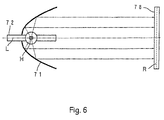
- Fig. 6 schematically depicts a conventional example optical device arrangement.
- This known optical device is composed of a parabolic reflector 71 and a light source lamp 72 which is located along a center axis L of this parabolic reflector 71.
- a liquid crystal cell 78 is located on area R to be illuminated by the above described optical device.
- the light emitted from the light source lamp 72 is, for the most part, focussed by means of parabolic reflector 71, and is emitted as parallel light beam onto illumination area R . Therefore, a high utilization factor of the light can be obtained.
- the light beam formed by means of the parabolic reflector 71 in the vicinity of its center has a high light flux density, while it has a low light flux density on its periphery. Therefore, the total surface of the area R to be illuminated cannot be illuminated with a uniform illumination intensity.
- Fig. 7 shows, in schematic form, a conventional example of the arrangement of a optical device B using an integrator lens.
- a first lens plate 73 on which several lens elements 74 are located, is arranged in front of parabolic reflector 71 on a plane perpendicular to center axis L of the above described parabolic reflector.
- a second lens plate 75 is arranged in front of the first lens plate 73 such that it is parallel to and spaced from the first lens plate 73.
- second lens plate 75 there are numerous lens elements 76, each of which corresponds to a lens element 74 on the first lens plate 73.
- second lens plate 75 is arranged such that respective lens element 76 is positioned in the respective focal point of corresponding lens element 74 of first lens plate 73.
- the light beam which is parallel to center axis L and which was formed by means of the parabolic reflector 71 is divided by respective lens element 74 of first lens plate 73 according to above described respective lens element 74 and this divided light is converged by corresponding respective lens element 76 on second lens plate 75.
- a real image of the emission part H of light source lamp 72 is formed on the respective lens element 76 of the second lens plate 75.
- the respective light which was converged by lens element 76 with second lens plate 75 is superimposed by the lens element 76 in the state in which the real image of emission part H is enlarged, in the same area R to be illuminated.
- the light flux density in the vicinity of the center has a small difference from the light flux density on the periphery due to the above described optical device. Furthermore, by means of second lens plate 75, the respective divided light is superimposed in the same area R to be illuminated. In this way, high uniformity of the illumination intensity can be obtained on the overall surface of above described illumination area R.
- Fig. 8 is a schematic of a arrangement of a liquid crystal projector device of the projection type for display of color images which has the optical device B with the configuration shown in Fig. 7.
- the light which emerges from each lens element 76 of the second lens plate 75 in the optical device 70 of the configuration shown in Fig. 7 is reflected by total reflex mirror 80a, then passes through a UV-IR-cut filter 81 which screens out ultraviolet radiation and infrared radiation reaches mirror 82.
- Mirror 82 is provided with a multilayer color separation film and the infrared radiation reaching this minor 82 is separated into a red component, a green component and a blue component.
- the light with the red component is emitted via total reflex minor 80b and condenser lens 84a onto a liquid crystal cell for red 85 which is located on a illumination area R1 .
- the light with the green component and the light with the blue component are separated by means of a mirror 83 having a multilayer color separation film, the light with the green component being emitted via condenser lens 84b onto a liquid crystal cell for green 86 which is located on area illumination area R2 .
- the light with the blue component is emitted via condenser lens 84c onto a liquid crystal cell for blue 87 which is located on an illumination area R3 .
- the light which emerges from respective lens element 76 of second lens plate 75 is separated in this way into the red component, the green component, and the blue component and then superimposed at liquid crystal cell for red 85, at liquid crystal cell for green 86, and liquid crystal cell for blue 87, respectively.
- the light with the red component and the light with the green component are combined by mirror 88 with a multilayer color synthesis film. Furthermore, this light is combined with the light with the blue component by mirror 89 which also has a multilayer color synthesis film. This combined light is emitted via projection lens 90 onto a suitable screen which is not shown in the drawing. In this way, a color image is projected on the above described screen.
- the metal halide lamp used as light source lamp 20 has high uniformity of the spectral energy distribution for light which is emitted from the entire emission part.
- the spectral distribution of the emitted light is, however, different according to the area of the emission part. This means that, in the center area of the emission part, the light ratio is large due to the mercury line, while in the peripheral area of the emission part, the light ratio with wavelengths that are greater than or equal to 600 nm is large due to molecular emission.
- the first object of the invention is to devise a optical device which has high uniformity of the illumination intensity on the entire surface of a area to be illuminated, and a small shape, and in which a high utilization factor of the light can be obtained.
- the second object of the invention is to devise an optical device in which light with high uniformity of the spectral distribution can be emitted.
- the third object of the invention is to devise a multisurface reflector which is used for the above described optical device.
- an optical device having a multisurface concave reflector which is composed of several mirror elements which each have an oval reflection surface, a light source lamp in which the emission part is arranged such that it is positioned along the center axis of the multisurface reflector, and a lens plate which is located in front of the multisurface reflector on a plane perpendicular to the center axis of thereof, and in which there are several lens elements, each of which correspond to the mirror elements in the multisurface reflector.
- a focal point is positioned in the emission part of the light source lamp, and another focal point is positioned for the corresponding mirror element in the lens plate, the light from the emission part of the light source lamp being divided by the respective mirror element for the multisurface reflector, and this divided respective light being superimposed by the respective mirror element in the lens plate in an area to be illuminated.
- the objects according to the invention are furthermore advantageously achieved by the above described lens plate being located on the side of the opening of the multisurface reflector in the optical device.
- the objects according to the invention are additionally advantageously achieved by the above described light source lamp being a metal halide lamp of the short arc type in the optical device.
- the object with respect to the reflector is also achieved by the fact that, in a multisurface reflector which is formed such that several mirror elements are arranged in a overall concave form which each mirror element has an oval reflection surface, in the above described several mirror elements, some focal points are positioned substantially at the same general location in which there is a light source, and that the other focal points are located on an essentially identical plane which is perpendicular to the center axis of the concave multisurface reflector forward thereof, and at the same time, that they are arranged such that they are positioned in the same arrangement as the arrangement of the mirror elements.
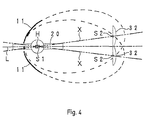
- Fig. 1 is a schematic of one example of the arrangement of the optical device A according to the invention.
- This arrangement comprises a concave multisurface reflector 10 and a light source lamp 20 having a roughly cylindrical emission part H located on center axis L of multisurface reflector 10 such that it is positioned along center axis L.
- the arrangement also includes a lens plate 30 which is located in front of multisurface reflector 10 on a plane that is perpendicular to the center axis L of the multisurface reflector 10.
- a body to be illuminated 40 is located on a illumination area R of the optical device A and which, for example, has a cornered shape, e.g., rectangular, in front of which a condenser lens 41 is positioned.
- multisurface reflector 10 is formed numerous mirror elements 11 (in the example shown in the drawing, 16) which combine to form a generally oval reflection surface having a overall concave shape as seen in Fig. 1.
- a suitable shape as viewed from the front of the multisurface reflector 10 is a cornered shape which is similar to body 40 which is to be illuminated and which is located in illumination area R .
- a metal halide lamp of the short arc type Dysprosium, indium, tin and the like are metal components which are encapsulated in the such a lamp, while iodine, bromine and the like are the halogen components.
- lens plate 30 comprises substrate 31 on which are disposed numerous lens elements 32 which correspond in number to the mirror elements 11 of the multisurface reflector 10. Lens elements 32 are each located on the surface of the side of substrate 31 which faces the illumination area R and are located immediately abutting one another.
- each mirror element 11 has a different slope with respect to the center axis L of the multisurface reflector 10.
- Some focal points S1 are positioned in essentially the identical place in which the light source is located.
- Other focal points S2 are located on a essentially identical place which is perpendicular to the center axis L of the multisurface reflector 10, and at the same time, they are arranged such that they are positioned in the same arrangement as the arrangement of mirror elements 11.
- each mirror element 11 has a focal point S1 positioned in the center of emission part H of light source lamp 20 and another focal point S2 which is positioned in an upper part of a corresponding lens element 32 of lens plate 30.
- the light emitted from the emission part H of the light source lamp 20 is divided by multisurface reflector 10 according to its respective mirror elements 11. This divided light is converged by corresponding lens element 32 of lens plate 30. In doing, so a real image of emission part H of light source lamp 20 is formed on the respective lens element 32 of lens plate 30.
- the respective light which has been converged by lens element 32 is superimposed by above described lens element 32 in the state in which the real image of emission part H is enlarged, in illumination area R .
- the light emerging from the location of the light source can be divided by mirror element 11 according to the measure by which the first focal points S1 of the various mirror elements 11 are each positioned at essentially the same place where the light source is located. Furthermore, the respective divided light can be converged according to the arrangement of mirror elements 11 at a different location on an essentially identical plane by the measure by which the second focal points S2 of minor elements 11 are located on an essentially identical plane which is oriented perpendicular to center axis L of multisurface reflector 10, and furthermore, by being positioned in the state in which they have the same arrangement as the arrangement of the mirror elements 11 and the lens elements 32.
- high uniformity of the illumination intensity can be obtained by the optical device due to the measure by which the light from emission part H of the light source lamp 20 is divided by the multisurface reflector 10, and furthermore, by the respective divided light being superimposed by the lens plate 30 in illumination area R on the entire surface of the area to be illuminated.
- the distance between multisurface reflector 10 and lens plate 30 can be reduced due to the fact that no additional lens plate is required between the multisurface reflector 10 and the lens plate 30. In this way, the dimension of the device in the direction of center axis L can be reduced. Furthermore, for each lens element 32 on lens plate 30, a real image of emission part H can be formed with a dimension which is less than the opening of the lens element 32. In this way, it is possible to prevent some of the light from multisurface reflector 10 from being lost, and as a result, a high utilization factor can be obtained.
- a metal halide lamp of the short arc type as light source lamp 20
- light having a high uniformity of the spectral energy distribution is emitted by the entire emission part H of the light source lamp 20.
- the equilibrium of the spectral energy can be maintained and therefore light with high uniformity of the spectral distribution can be emitted.
- lens plate 30 can be located directly over the opening of the multisurface reflector 10, as is shown in Fig. 5.
- the distance between the multisurface reflector 10 and the lens plate 30 becomes extremely small. Furthermore, the size of the entire optical device can be reduced.
- the minor elements 13 can be arranged such that light reflected by them directly irradiates the body 40 to be illuminated (as can be seen for the uppermost ray passing from reflector 10 to body 40 in Fig. 5). In this case, there is no problem in practice since the uniformity of the illumination intensity can be ensured by means of mirror elements 11.
- optical device A with the configuration shown in Fig. 1 can be produced:
- the illumination intensity in illumination area R was roughly 1,700,000 lux.
- the uniformity of the illumination intensity on the entire surface of above described illumination area R was roughly 1,700,000 lux.
- the light which irradiates illumination area R has the same spectral distribution as the light emitted directly from light source 20.
- the light source device B shown in Fig. 7 was produced and actuated for comparison purposes. In doing so, the uniformity of the illumination intensity on the entire surface of illumination area R was high, with the illumination intensity in the illumination area R being roughly 1,300,000 lux. However, the light utilization factor for device B as compared to light source device A was lower. Furthermore, for the light which irradiates illumination area R , the ratio of the red component with wavelengths of greater than or equal to 600 nm compared to the light emitted directly by light source lamp 20 was smaller for device B .
- the optical device By means of the optical device according to the invention high uniformity of the illumination intensity on the entire surface of the area to be illuminated can be obtained, the size of the entire device can be reduced, and at the same time a high light utilization factor can be obtained.
- the entire device can be made even smaller by the arrangement of the lens plate on the side of the opening of the multisurface reflector.
Landscapes
- Physics & Mathematics (AREA)
- Engineering & Computer Science (AREA)
- General Engineering & Computer Science (AREA)
- General Physics & Mathematics (AREA)
- Optics & Photonics (AREA)
- Projection Apparatus (AREA)
Applications Claiming Priority (2)
| Application Number | Priority Date | Filing Date | Title |
|---|---|---|---|
| JP7342093A JPH09185008A (ja) | 1995-12-28 | 1995-12-28 | 光学装置および多面反射鏡 |
| JP342093/95 | 1995-12-28 |
Publications (1)
| Publication Number | Publication Date |
|---|---|
| EP0783116A1 true EP0783116A1 (fr) | 1997-07-09 |
Family
ID=18351108
Family Applications (1)
| Application Number | Title | Priority Date | Filing Date |
|---|---|---|---|
| EP96120879A Withdrawn EP0783116A1 (fr) | 1995-12-28 | 1996-12-24 | Dispositif optique et réflecteur multisurface |
Country Status (3)
| Country | Link |
|---|---|
| US (1) | US5971568A (fr) |
| EP (1) | EP0783116A1 (fr) |
| JP (1) | JPH09185008A (fr) |
Cited By (5)
| Publication number | Priority date | Publication date | Assignee | Title |
|---|---|---|---|---|
| DE19737549A1 (de) * | 1996-09-20 | 1998-03-26 | Valeo Vision | Signalleuchte mit einem Spiegel mit gerillter Oberfläche |
| EP0985875A2 (fr) | 1998-09-08 | 2000-03-15 | Ushiodenki Kabushiki Kaisha | Dispositif d' éclairage |
| AT500415B1 (de) * | 2001-03-13 | 2006-04-15 | Zizala Lichtsysteme Gmbh | Fahrzeugscheinwerfer |
| FR2896203A1 (fr) * | 2006-01-18 | 2007-07-20 | Peugeot Citroen Automobiles Sa | Feu de signalisation a motifs catadioptriques pour vehicule automobile. |
| EP1905605A1 (fr) * | 2006-09-27 | 2008-04-02 | Ushiodenki Kabushiki Kaisha | Dispositif d'irradiation de lumière et imprimante à jet d'encre |
Families Citing this family (7)
| Publication number | Priority date | Publication date | Assignee | Title |
|---|---|---|---|---|
| JP3903091B2 (ja) * | 1997-06-30 | 2007-04-11 | 富士フイルム株式会社 | 画像読取装置 |
| DE69826950T2 (de) * | 1997-09-05 | 2006-02-23 | Sharp K.K. | Dunkelfeld-Projektionsanzeigegerät |
| US6488395B2 (en) * | 1998-01-30 | 2002-12-03 | Federal-Mogul World Wide, Inc. | Low profile lighting |
| JP2945376B1 (ja) * | 1998-05-01 | 1999-09-06 | スタンレー電気株式会社 | 灯 具 |
| US20040026602A1 (en) * | 2002-08-08 | 2004-02-12 | Tsung-Yin Chen | Adjustable light converging device |
| US20080174990A1 (en) * | 2006-10-24 | 2008-07-24 | Tuck Richard G | Optical system with segmented and/or flexible reflector |
| JP2010140888A (ja) * | 2008-11-14 | 2010-06-24 | Seiko Epson Corp | 照明装置、プロジェクタ |
Citations (7)
| Publication number | Priority date | Publication date | Assignee | Title |
|---|---|---|---|---|
| US2186123A (en) | 1937-01-27 | 1940-01-09 | Zeiss Ikon Ag | Illuminating system |
| US3449561A (en) * | 1967-07-03 | 1969-06-10 | Textron Electronics Inc | Aconic collector |
| GB2040431A (en) * | 1978-12-20 | 1980-08-28 | Zeiss Jena Veb Carl | Illumination system for photo-copying devices |
| US4234247A (en) * | 1978-10-30 | 1980-11-18 | Corning Glass Works | Method of making a reflector |
| US4916585A (en) * | 1988-04-04 | 1990-04-10 | Koito Seisakusho Co., Ltd. | Headlight device for vehicle |
| EP0563874A1 (fr) * | 1992-03-31 | 1993-10-06 | Matsushita Electric Industrial Co., Ltd. | Système d'éclairage optique et dispositif d'affichage par projection l'utilisant |
| WO1994015143A1 (fr) * | 1992-12-21 | 1994-07-07 | Miroslav Hanecka | Systeme d'eclairage pour spots, projecteurs et appareils d'agrandissement |
Family Cites Families (3)
| Publication number | Priority date | Publication date | Assignee | Title |
|---|---|---|---|---|
| JPH0317362Y2 (fr) * | 1986-07-10 | 1991-04-12 | ||
| JP3207087B2 (ja) * | 1995-07-28 | 2001-09-10 | 株式会社小糸製作所 | 車輌用灯具 |
| JP3185127B2 (ja) * | 1995-07-28 | 2001-07-09 | 株式会社小糸製作所 | 車輌用灯具 |
-
1995
- 1995-12-28 JP JP7342093A patent/JPH09185008A/ja active Pending
-
1996
- 1996-12-24 EP EP96120879A patent/EP0783116A1/fr not_active Withdrawn
- 1996-12-30 US US08/775,094 patent/US5971568A/en not_active Expired - Lifetime
Patent Citations (7)
| Publication number | Priority date | Publication date | Assignee | Title |
|---|---|---|---|---|
| US2186123A (en) | 1937-01-27 | 1940-01-09 | Zeiss Ikon Ag | Illuminating system |
| US3449561A (en) * | 1967-07-03 | 1969-06-10 | Textron Electronics Inc | Aconic collector |
| US4234247A (en) * | 1978-10-30 | 1980-11-18 | Corning Glass Works | Method of making a reflector |
| GB2040431A (en) * | 1978-12-20 | 1980-08-28 | Zeiss Jena Veb Carl | Illumination system for photo-copying devices |
| US4916585A (en) * | 1988-04-04 | 1990-04-10 | Koito Seisakusho Co., Ltd. | Headlight device for vehicle |
| EP0563874A1 (fr) * | 1992-03-31 | 1993-10-06 | Matsushita Electric Industrial Co., Ltd. | Système d'éclairage optique et dispositif d'affichage par projection l'utilisant |
| WO1994015143A1 (fr) * | 1992-12-21 | 1994-07-07 | Miroslav Hanecka | Systeme d'eclairage pour spots, projecteurs et appareils d'agrandissement |
Cited By (7)
| Publication number | Priority date | Publication date | Assignee | Title |
|---|---|---|---|---|
| DE19737549A1 (de) * | 1996-09-20 | 1998-03-26 | Valeo Vision | Signalleuchte mit einem Spiegel mit gerillter Oberfläche |
| EP0985875A2 (fr) | 1998-09-08 | 2000-03-15 | Ushiodenki Kabushiki Kaisha | Dispositif d' éclairage |
| AT500415B1 (de) * | 2001-03-13 | 2006-04-15 | Zizala Lichtsysteme Gmbh | Fahrzeugscheinwerfer |
| FR2896203A1 (fr) * | 2006-01-18 | 2007-07-20 | Peugeot Citroen Automobiles Sa | Feu de signalisation a motifs catadioptriques pour vehicule automobile. |
| EP1905605A1 (fr) * | 2006-09-27 | 2008-04-02 | Ushiodenki Kabushiki Kaisha | Dispositif d'irradiation de lumière et imprimante à jet d'encre |
| CN101152784B (zh) * | 2006-09-27 | 2010-11-10 | 优志旺电机株式会社 | 光照射器及喷墨打印机 |
| US7934802B2 (en) | 2006-09-27 | 2011-05-03 | Ushiodenki Kabushiki Kaisha | Light irradiation device and inkjet printer |
Also Published As
| Publication number | Publication date |
|---|---|
| US5971568A (en) | 1999-10-26 |
| JPH09185008A (ja) | 1997-07-15 |
Similar Documents
| Publication | Publication Date | Title |
|---|---|---|
| EP0883302B1 (fr) | Dispositif d'affichage à cristaux liquides du type à projection | |
| EP0239007B1 (fr) | Projecteur à cristaux liquides | |
| US5046837A (en) | Illumination system | |
| US5607229A (en) | Illumination system including an asymmetrical projection reflector | |
| US5971568A (en) | Optical device and multisurface reflector | |
| US6392809B2 (en) | Array lens, lighting optical system, optical unit and imaging apparatus | |
| JPH05142653A (ja) | 照明装置 | |
| JP3182863B2 (ja) | 投射型表示装置 | |
| JP3392084B2 (ja) | 投射装置 | |
| US5311227A (en) | Liquid crystal projection display device with mirror | |
| US6089720A (en) | Illuminating optical apparatus | |
| JP2903485B2 (ja) | 投影装置 | |
| US20060126031A1 (en) | Illumination optical system of projection apparatus | |
| US5617152A (en) | Projector system for video and computer generated information | |
| EP0631434A1 (fr) | Projecteur | |
| JP2002196302A (ja) | 投射型表示装置およびそれを用いたマルチ画面表示装置 | |
| JP3413099B2 (ja) | 液晶プロジェクタの照明装置 | |
| US6705730B2 (en) | Picture display device | |
| KR100352974B1 (ko) | 칼라드럼을 이용한 화상투사 장치 | |
| JPH07270747A (ja) | 投写型表示装置 | |
| JPH02275933A (ja) | 液晶プロジェクタ | |
| JPH0815701A (ja) | 投射型液晶表示装置用照明装置、及びこれを用いた液晶表示装置 | |
| KR960014292B1 (ko) | 단판식 액정표시소자 투영기 | |
| US7798654B2 (en) | Image display apparatus | |
| JPH09105899A (ja) | 投射型表示装置 |
Legal Events
| Date | Code | Title | Description |
|---|---|---|---|
| PUAI | Public reference made under article 153(3) epc to a published international application that has entered the european phase |
Free format text: ORIGINAL CODE: 0009012 |
|
| AK | Designated contracting states |
Kind code of ref document: A1 Designated state(s): DE GB NL |
|
| 17P | Request for examination filed |
Effective date: 19970702 |
|
| 17Q | First examination report despatched |
Effective date: 20010122 |
|
| STAA | Information on the status of an ep patent application or granted ep patent |
Free format text: STATUS: THE APPLICATION IS DEEMED TO BE WITHDRAWN |
|
| 18D | Application deemed to be withdrawn |
Effective date: 20010602 |