EP0783170B1 - Appareil et procédé pour l'acquisition et l'analyse d'une distribution spatiale de points discrets - Google Patents
Appareil et procédé pour l'acquisition et l'analyse d'une distribution spatiale de points discrets Download PDFInfo
- Publication number
- EP0783170B1 EP0783170B1 EP96100070A EP96100070A EP0783170B1 EP 0783170 B1 EP0783170 B1 EP 0783170B1 EP 96100070 A EP96100070 A EP 96100070A EP 96100070 A EP96100070 A EP 96100070A EP 0783170 B1 EP0783170 B1 EP 0783170B1
- Authority
- EP
- European Patent Office
- Prior art keywords
- failure
- coordinate
- pattern
- predetermined
- point
- Prior art date
- Legal status (The legal status is an assumption and is not a legal conclusion. Google has not performed a legal analysis and makes no representation as to the accuracy of the status listed.)
- Expired - Lifetime
Links
Images


Classifications
-
- G—PHYSICS
- G11—INFORMATION STORAGE
- G11C—STATIC STORES
- G11C29/00—Checking stores for correct operation ; Subsequent repair; Testing stores during standby or offline operation
-
- H—ELECTRICITY
- H10—SEMICONDUCTOR DEVICES; ELECTRIC SOLID-STATE DEVICES NOT OTHERWISE PROVIDED FOR
- H10P—GENERIC PROCESSES OR APPARATUS FOR THE MANUFACTURE OR TREATMENT OF DEVICES COVERED BY CLASS H10
- H10P74/00—Testing or measuring during manufacture or treatment of wafers, substrates or devices
- H10P74/23—Testing or measuring during manufacture or treatment of wafers, substrates or devices characterised by multiple measurements, corrections, marking or sorting processes
-
- G—PHYSICS
- G01—MEASURING; TESTING
- G01R—MEASURING ELECTRIC VARIABLES; MEASURING MAGNETIC VARIABLES
- G01R13/00—Arrangements for displaying electric variables or waveforms
- G01R13/20—Cathode-ray oscilloscopes
- G01R13/206—Arrangements for obtaining a 3- dimensional representation
-
- G—PHYSICS
- G01—MEASURING; TESTING
- G01R—MEASURING ELECTRIC VARIABLES; MEASURING MAGNETIC VARIABLES
- G01R31/00—Arrangements for testing electric properties; Arrangements for locating electric faults; Arrangements for electrical testing characterised by what is being tested not provided for elsewhere
- G01R31/28—Testing of electronic circuits, e.g. by signal tracer
- G01R31/317—Testing of digital circuits
- G01R31/3181—Functional testing
- G01R31/319—Tester hardware, i.e. output processing circuits
- G01R31/31903—Tester hardware, i.e. output processing circuits tester configuration
- G01R31/31912—Tester/user interface
-
- Y—GENERAL TAGGING OF NEW TECHNOLOGICAL DEVELOPMENTS; GENERAL TAGGING OF CROSS-SECTIONAL TECHNOLOGIES SPANNING OVER SEVERAL SECTIONS OF THE IPC; TECHNICAL SUBJECTS COVERED BY FORMER USPC CROSS-REFERENCE ART COLLECTIONS [XRACs] AND DIGESTS
- Y10—TECHNICAL SUBJECTS COVERED BY FORMER USPC
- Y10S—TECHNICAL SUBJECTS COVERED BY FORMER USPC CROSS-REFERENCE ART COLLECTIONS [XRACs] AND DIGESTS
- Y10S706/00—Data processing: artificial intelligence
- Y10S706/902—Application using ai with detail of the ai system
- Y10S706/911—Nonmedical diagnostics
- Y10S706/916—Electronic or computer, internal or network, circuit
Definitions
- the invention relates to an apparatus and a method to capture and evaluate one in a multidimensional Coordinate system arranged spatially discrete Dot pattern, each dot of the pattern being at least two distinguishable state values.
- the invention relates to an apparatus and a method for Detection and classification of the binary failure patterns of defective memory cells of a semiconductor memory.
- the failure patterns of the memory cells of defective semiconductor memories provide information about the technology problems underlying the failures when manufacturing the semiconductor memories.
- non-statistical distributions of the failure patterns on a wafer after evaluation give suitable indications of systematic technology and process problems.
- One of the difficulties here is that failure patterns can occur in a wide variety of new variants.
- the raw data quantities on which the analysis is based and obtained using chip test systems are enormous.
- the preprocessed data were transmitted as a raw file from the measuring device to a computer and subjected to a main analysis created using conventional programming technology.
- a major disadvantage of this procedure was also that considerable parts of the preliminary and main analysis had to be reprogrammed when changing over to a new memory generation. Likewise, types of failure patterns that had to be analyzed had to be reprogrammed with great effort.
- a device for detecting and evaluating one is Test measurements on an apparatus obtained from its failure pattern Components known, this device comprises in detail: a Measuring device (1,2) for obtaining and storing the raw data; one to Memory-assigned computer (3) in which the stored data are entered, and in which a feature extractor (features extraction) is provided, which processes the raw data according to certain characteristics and outputs the result in a computing vector; one assigned to the computer Neural network (4), in which the computing vector as an input vector is entered and which by comparing the input vector with Default vectors compute an output vector, and a classification value (diagnosis) of the measured failure pattern based on the determined Assigns and outputs output vector.
- a classification value diagnosis
- the invention has for its object a device and a method for recording and evaluating a spatial discrete dot pattern, such as a failure pattern in particular to provide a semiconductor memory chip, which or which also with a considerable number of points, especially in the range of greater than 1 mega, one automatically and with high reliability and reproducibility analysis and classification of the dot pattern to be carried out with usable analysis times.
- a spatial discrete dot pattern such as a failure pattern in particular to provide a semiconductor memory chip, which or which also with a considerable number of points, especially in the range of greater than 1 mega, one automatically and with high reliability and reproducibility analysis and classification of the dot pattern to be carried out with usable analysis times.
- the analysis of the spatial discrete dot pattern by means of a implemented in a computer neural network is carried out, the one n-dimensional input vector with n components for analysis is offered, and which by comparing the input vector with saved, based on sample point patterns default vectors obtained an output vector computes one to classify the dot pattern Classification value of the measured dot pattern based on the outputs determined output vector.
- the neural network places an arrangement between one another linked processing elements, so-called Neurons, which are in a hierarchical structure are arranged on several levels. Every neuron can have one or have multiple inputs, and usually have only one Output.
- the preferred neural network is used from three different levels: one the input vector assigned input level, an assigned to the output vector Output level, and one between the input level and the Output level arranged computing level assigned to the default vectors.
- the number of neurons in the calculation level depends among other things on the complexity of the neural network for the detection of presented dot patterns, the desired information capacity of the network, the number and extent of the skills trained neural network to process unknown patterns, and the number of iterations that the neural network Performed in the training phase to achieve all of the desired To provide network directions and basic values.
- the neural network When the neural network is trained, it becomes successive presents predetermined input data patterns that so-called sample dot pattern.
- the values of the basic neuronal values in this way in the neural network set that the output of the network for each one Training pattern at least roughly with a desired one corresponding network output (target vector or output vector) for the corresponding pattern. After Completion of the training will be all basic values fixed at their current values.
- the neural network can then be used in principle for Detection of unknown patterns can be used.
- Pattern recognition becomes that from the unknown point patterns input vectors obtained by algorithmic preprocessing successively applied to the inputs of the network, and corresponding network responses from output the output node.
- the neural network is a type Restricted Coulomb Energy network.
- Restricted Coulomb Energy refers to an energy function based on an electrostatic potential.
- the RCE network is a trademark of the company Nestor protected, which is a Nobel Prize winner company L.N. Cooper is.
- An RCE-type neural network has exactly three levels, an input layer a computing level ("hidden layer"), and an output level ("output layer").
- the computing level is complete with the Input level connected.
- the output level is partial connected to the computing level. The reason for this is in that different types of processing elements be used in the computing and output levels.
- RCE networks work because of their simpler Arrangement very quickly and efficiently.
- this type of Input level of the neural network is an n-dimensional Input vector made from a sample point pattern of a known one Class obtained by preprocessing, presented, where the input vector is a target point in an n-dimensional Represents space.
- the input level linked computing level of the neural RCE network is around the target point of each input vector is an n-dimensional space (Hypersphere or hypercube) with the target point of the Input vector as the center of the n-dimensional space fixed, with the volume of this room area accordingly the class to be assigned. All Spaces within this n-dimensional area thus belong to the predetermined, the respective sample point pattern belonging class. This procedure comes with other input vectors belonging to other classes, repeated.
- the neural network determines whether one is related to a particular one Class-related input vector within the space an input vector belonging to another class lies. If this is the case, the corresponding Spaces through geometric adjustment or tapering so far changed that one belonging to a certain class Input vector not within one to one space input class belonging to another class, although it may well be the case that some the room areas, including those of different classes, overlap in areas.
- Hyperquader uses what in contrast to using hyperspheres as spatial areas a certain class has the advantage that in the case of a Adapting the room areas not tapering every dimension must become. In the case of using hyperspheres, the Volume decrease in the area always with a taper larger than with Hyperquadern. So that is the possibility of Generalization, which is an important property of neural Networks represents less favorable than in the case of Cuboids.
- RCE networks An advantage of RCE networks continues to exist in general in that this automatically occurs during the training procedure can be configured.
- the training procedure combines the Configuration and learning through the use of the leading Algorithm.
- the number of processing units (“Hidden units") in the computing level of the neural network automatically set.
- Sample sizes can be sized through the training procedure or expansion of the room areas can be adjusted more easily.
- An essential feature of the invention is that neural network not the original, physically measured Coordinate and state values of each point of the multi-dimensional spatial dot pattern are offered, but first of all there are coordinate counters or coordinate projections for each coordinate value of a coordinate axis calculated from the original data, the value of the Coordinate counter from the number of points recorded Dot pattern of the corresponding coordinate with a predetermined one State value is calculated.
- the actual pattern recognition by means of the neural network takes place on the Basis of the determined coordinate counter instead. To this Ways become when recording the coordinate values and state values of each point by means of the measuring device resulting raw data quantities compressed considerably.
- a single point defect in the case of a Semiconductor memory is an electrical failure in which both the x and y coordinates are known in principle
- the neural network does not have Coordinate counter presented directly as input vectors, but an n-dimensional input vector, the Number n typically on the order of about 10 to is about 30 where the n components of the input vector through a series of sub-procedures from the values of the coordinate counters of the spatially discrete dot pattern become.
- the assigned to the n components of the n-dimensional input vector numerical values are standardized, especially in the numerical range between -1 and +1.
- the multi-dimensional coordinate system of the spatially discrete point pattern orthogonal coordinate axes in particular has two orthogonal coordinate axes, and the value of each coordinate counter by adding up the detected points of each coordinate with a predetermined one Condition value and projection onto the corresponding one orthogonal coordinate axis, in particular column axis and Row axis is formed.
- the dot pattern is the failure pattern of a physical contiguous block of memory cells
- Semiconductor memory from a variety on the main surface of a semiconductor wafer formed semiconductor memories represents.
- Each failure cell has the failure pattern one of three state values, one of which is a state value a zero failure of the memory cell, a state value a one failure of the memory cell and a state value one Zero and one failure of the memory cell is assigned.
- the memory cells are on the main surface of the semiconductor wafer formed semiconductor memory in Bit lines or columns and in rows or word lines Arranged in a matrix, and set the coordinate counters each represent a column counter and a row counter.
- the invention enables through the use of a neural Network a reliable classification of memory chip failure patterns, which also parallel to the usual function test memory chips during a standard production measurement can be carried out.
- the preprocessing algorithm to provide the input data for the neural Network and the neural network itself are scalable and thus enables the use of the software used with a transition from one chip generation to the next, without that this would have to be reprogrammed.
- the analysis program can be an inexpensive Computer, for example a commercially available personal computer (PC) can be used, for example, via an interface card with the computer or the microprocessor of the Chip test system is connected. It is also possible by bringing out the data and address bus system in parallel, via which the microprocessor of the chip test system communicates with the fail memory of the test system to which Interface card of the PC's failure pattern in the fail memory parallel to its processing in the chip test system in the separate read in the arranged PC and process it there.
- PC personal computer
- a preferred embodiment is the Invention shown, in which the failure pattern of the memory cells a defective dynamic semiconductor memory from Type 4 Mega can be examined.
- the invention is self-evident for the analysis of larger semiconductor memories, for example 16 mega, 256 mega and more possible; In some places, special features are required the following description separately.
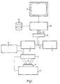
- FIG. 1 shows a schematic View more details of the pattern recognition system according to the invention. It is a programmable wafer tester 1 and a measuring probe device 2 assigned to it Measuring tips 3 as components of an automatic parametric Chip test system for measuring those manufactured on a wafer 4 DRAM memory chips provided. To the measuring device A large number of measuring instruments are connected 5 for recording and evaluating the electrical properties of the memory chips arranged on the wafer 4. To control the individual components of the measuring system a control processor 6 is provided, which for storage and pre-processing of the data associated with a fail memory 7 is.
- the control processor 6 of the measuring device communicates with the fail memory 7 via a data and address bus 8 which an interface card 9 is connected, via the the raw data from the fail memory 7 via lines 13 into one separate computer 10 can be read for further processing.
- the further processing of those read into the computer 10 Raw data is not done by algorhythmic as before Decomposing the measured failure patterns with conventional ones Programming technology, but more characteristic by extraction Characteristics from the dropout pattern and presentation of these characteristics as an input vector for a trained within the computer 10 neural network, which then the Classification of the entered failure pattern takes over how is explained in more detail below.
- the computer 10 is a display device such as associated with a screen 11 on which analyzed by means of the computer 10 Failure patterns and the result of the classification are displayed can be.
- the computer 10 also has a data memory 12 assigned to store the raw data and the processed data.
- Re 1 Measurement of the semiconductor chips of a wafer, processing the measured data, reading in the measured raw data, and processing the raw data for further analysis.
- measuring probe device 2 with Measuring tips 3 When measuring the chip failures by means of the measuring device consisting of the Prober 1, measuring probe device 2 with Measuring tips 3, measuring instruments 5, and processor 6 and fail Memory 7 are first of all semiconductor memory chips of the 6 "semiconductor wafer 2, the x and y coordinates of each individual chips on the wafer 2, as well as information about Current-voltage values of the chips (e.g. pass / fail information via an operation or stand-by current, generator voltages and the like) by means of the measuring device determined and for each chip the failure pattern and the Default rate, i.e. the percentage of total failure cells present measured.
- Current-voltage values of the chips e.g. pass / fail information via an operation or stand-by current, generator voltages and the like
- FIG. 2 shows a schematic Top view of a physical block 14 of a semiconductor memory chip with 256 word lines WL1 to WL256 and 1024 bit lines BL1 to BL1024.
- the memory cells of the Chips are each at the intersection of a word line WLn and a bit line BLm arranged.
- Figure 2 there are some typical ones Arrangements of faulty memory cells are shown.
- reference numerals 15, 16 denote 17 individually failed at the associated word-bit line crossing Single cells (single bit failures), the reference numbers 18 and 19 immediately adjacent falling single cells (pairwise bit failure), the reference numbers 20, 21, 22, 23 side by side failed on part of a word line Memory cells, with the word line failure 20 additionally another separate failure 24 with another Failure state than in the other failure cells
- Word line 20 is shown
- the reference numeral 25 denotes an accumulation of adjacent failure cells (so-called cluster)
- the reference number 26 a failure of several adjacent bit lines
- the one generated by the measuring device or the chip test system binary raw file with information for a wafer or at Block measurements for one lot, i.e. one due to production associated group of several identical wafers as a raw data file via lines 13 (see FIG. 1) in read the computer 10.
- header information such as lot number, wafer number and assigned Design type.
- a chip information consists of a chip info block, followed by 16 hexadecimal information (so with the 4 mega semiconductor chip) or 512 segment information (so with 16 mega semiconductor memory).
- the chip info block shows that the data for one follow a specific chip, namely the x and y coordinates the chip on the wafer, as well as technical information, for example information about current-voltage values of the chip.
- Hexadecimal information indicates that now the data for a new hexadecimal follows, namely the Hexadecimal number (with 4 mega semiconductor memory) or the Segment number (with 16 mega semiconductor memory), and there then a number of 256 word line counters or Column counters and 1024 bit line counters or line counters for total failure, and a corresponding number of coordinate counters for zero failures and one failures.
- the failure patterns of a chip were all x and y coordinates of the failure cells and the underlying Failure condition determined.
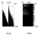
- each physical block 1 of the semiconductor chip a number of 256 line counters ZZ1 to ZZ256 and determined a number of 1024 column counters SZ1 to SZ1024, each of which is information alongside the number of the assigned row 1 to 256 or column 1 to 1024 the number the total occurring on this row or column Failure cells for each of the three failure states are included.
- the Coordinate counters thus give the projected onto the coordinate Total values of all failures with a certain failure condition (i.e. '0', '1', or '0' and '1') of the assigned Management again ("projection").
- the main global, i.e. related to an entire wafer Data structures are the following dynamically created Arrays. You can directly for the 4 mega semiconductor memory taken from the hexadecimal information of the raw data file be while for the 16 mega semiconductor memory from the segment information - modified accordingly - compiled become. Obtain the following explanations each on the 4 megabit chip, however, apply analogously also for a 16 megabit semiconductor memory. For customization of the analysis method according to the invention on chip generations larger or smaller 4 megabits are essentially required just changing some global constants that are defined in a predetermined program unit, and the adaptation of the program unit to generate the physical Blocks from the column and row counters of the raw data file.
- Echoes are only searched for if the corresponding one Hexadecant is not a total failure because then would have any failing word line and bit line projection in the other hexadecimal an echo, respectively if the respective failure patterns are not too chaotic Have character. Will a line in the corresponding Hexadecanals recognized as echo, so the line is off the central data structures and it will Flag signal flg [x, 5] of that line causing it for the echo is set to a value 'true'. In line elimination it should be taken into account that for example a failing bit line in the word line projection on each array element the line counter of the even one and odd hexadecimal edges projected with the value one becomes.
- the echo projection should not only be used in Bit line direction are eliminated, but it should be in the Echo hexadecants additionally the 256 projections with the Value one on the word line projection can be eliminated.
- a so-called baseline is the knowledge of the baseline widths in the elimination process requirement in both projection directions. The baseline widths are determined before each elimination. Lines are only eliminated up to the current one Baseline. The considerations made above to the echo problem are omitted if - conditionally, for example through the chip design - no echoes can occur, or consideration of echoes is not desired for other reasons or is required.
- FIGS. 3A to 3F "massive" failure pattern of a physical block shown, each figure consists of two halves, in the right half to the right the values of Column counters from SZ 1 to SZ 1024 to the right, and on the the left half of the screen shows the values of the line counters from ZZ 1 to ZZ 256 are plotted upwards.
- the typical shown Failure patterns represent part of the classes used to assess the failure mechanisms; indeed the number of such classes is typically around 70 or more.
- the actual sample classification is started.
- two different analysis methods used: a first neural network NN1 for analysis of a physical block with errors massive error, and a second neural network NN2 for the analysis of a faulty physical block regarding errors with low error mass.
- the usage different methods depending on the initially measured Failure rate is in terms of speed the analysis or optimization of the determined classification results performed. It should be taken into account that the use of a neural network in particular with large amounts of data the advantage of a considerably larger one Computing speed offers, however, with a considerable Loss of information is connected.
- the automatic pattern recognition process with conventional ones Methods a long computing time or high Occupancy rate of the computer is required, however, it can in turn more information will be obtained.
- step S1 all are first raw data obtained from the measuring device into the computer 10 entered and the failure rate FC ("Fail Count") of the ratio of the defective memory cells calculated for the total number. If the failure rate FC at step S2 is determined to be greater than about 99% in step S3 a total failure of the semiconductor chip is assumed and the process goes directly to a result section via branch 29 30 of the main program. If the default rate is FC at step S2 is determined to be less than 99%, branches the program to step S4, in which using the first neural network NN1 an analysis of the failure patterns and classification is carried out. If the classification succeeds, the method goes directly via branch 29 continue to section 30 of the main program.
- FC Failure Rate
- step S5 If a classification is not possible in step S5 is in a further branch a fine analysis again carried out; namely, an analysis and Classification of the failure pattern using a second neural network NN2 performed. If one The procedure is successful if the failure patterns are classified to section 30 of the main program in which the determined Category of the failure pattern is output. If a classification does not succeed, this becomes in step S7 determined and in section 30 a non-classifiable category spent.
- the first neural network NN1 decides on submission this input vector, what class of error the Failure acts or gives the failure for further processing free if there is no massive error class.
- First neural network NN1 is an arrangement of RCE type used, the principle of its operation is schematic based on a geometric interpretation according to the figures 5 and 6, and Figures 7A and 7B is explained.
- the neural network NN1 implemented in the computer 10 5 of the RCE type has three levels, one input level 31, a computing level 32, and an output level 33 Input level 31 has a number of 27 processing elements X1 to X27, each of which has a component E1 to E27 of the 27-dimensional input vector is assigned.
- the Processing elements X1 to X27 of the input level 31 is one Variety of processing elements Y1 to Ym of the computing level 32 assigned, the number m of processing elements Y of the computing level 32 is generally much larger as the dimension n of the input vector, and for example on the complexity of the calculation and classification of the analyzing dot pattern depends.
- At computing level 32 a 27-dimensional arrangement of not necessarily coherent spatial areas formed, the spatial form complex decision areas.
- FIG. 6 is a first component E1 of the right Input vector, and up a second component E2 of the Input vector plotted.
- E1 and E2 of the input vector Hyperspheres shown in two dimensions Case simply circles
- FIG. 6 are just two classes A and B for simplicity with the corresponding associated room areas schematically shown.
- circles or spatial areas 34, 35, 36, 37, 38 are shown, which are assigned to class A, and circles or spatial areas 39, 40, 41, 42, 43 that the Class B can be assigned.
- the arrangement of the room areas, i.e. their centers and their respective extent in Space taking into account the assignment to a specific Class is determined after training the neural network selected sample pattern.
- the Computing level 32 of the neural network NN1 is the one in the Input level 31 entered 27-dimensional input vector accordingly evaluates the arrangement of hyperspheres, related to a particular class, it belongs. If such Assignment to a certain class succeeds in the the output level 33 assigned to the computing level 32 accordingly determined class issued.
- the number of outputs Z1 and Z2 of the output level 33 corresponds essentially to that Number of classes specified. With the schematic explanation according to FIGS. 5 and 6, only two classes are A and B and correspondingly two output elements Z1 and Z2 of Output level 33 shown; in reality the number is of the classes or the number of output elements more than about 70.
- FIG. 7A shows the case in which the respective Classes A and B belonging to areas 44 and 45 of the Input vectors 46 and 47 do not overlap. In this case is a unique assignment of one at the input level 31 of the neural network to a test vector certain class A or B possible.
- figure shows 7B shows the case of two overlapping spatial areas 48 and 49; in this case, the neural training procedure Network within the computing level 32 which is the vector 50 and 51 orderly arranged room areas 48 and 49 to the extent i.e. to rejuvenate that there is no longer any overlap.
- the exam can be started any existing, special distributions of Error classes can be made over the entire wafer.
- One third neural network will be 22 different Distributions of failure patterns on the wafer that trained
- the following topographies can include: Accumulation defective chips over the entire edge of the wafer on which left or right edge of the wafer, accumulation defective Chips in the upper / lower and upper / lower lateral edge area of the wafer, accumulation of defective chips in the area of the Flat or anti-flat of the wafer, accumulation of faulty chips in a central ring area of the wafer, and the like.
- Distinctive distributions but not specially learned by the network from the third neural network with a Question marks classified. It is in the Usually either around particularly massive error classes over the entire wafer or around massive clustering of errors an error class, such as that caused by ill-treatment (Scratches) on the wafers.
- an error class such as that caused by ill-treatment (Scratches) on the wafers.
Landscapes
- Physics & Mathematics (AREA)
- General Physics & Mathematics (AREA)
- Engineering & Computer Science (AREA)
- Human Computer Interaction (AREA)
- General Engineering & Computer Science (AREA)
- Testing Or Measuring Of Semiconductors Or The Like (AREA)
- Image Analysis (AREA)
- Image Processing (AREA)
- For Increasing The Reliability Of Semiconductor Memories (AREA)
- Tests Of Electronic Circuits (AREA)
- Test And Diagnosis Of Digital Computers (AREA)
- Character Discrimination (AREA)
Claims (18)
- Dispositif pour la saisie et l'analyse d'une distribution spatiale de points discrets répartis dans un système de coordonnées à plusieurs dimensions, chaque point de la distribution pouvant prendre au moins deux valeurs d'état différentes, et comportant:un dispositif de mesure (1, 2, 3, 5, 6) pour enregistrer les valeurs de coordonnées et les valeurs d'état de chaque point de la distribution spatiale de points discrets à plusieurs dimensions,une mémoire (7) pour mémoriser les données qui correspondent aux valeurs de coordonnées et aux valeurs d'état enregistrées pour chaque point de la distribution spatiale de points discrets à plusieurs dimensions,un ordinateur (6, 10), associé à la mémoire (7), dans lequel on entre les données mémorisées et avec lequel on détermine, à partir des données mémorisées, un numérateur de coordonnées (SZ1 - SZ1024, ZZ1 - ZZ256) pour chaque valeur de coordonnée d'un axe de coordonnées, la valeur du numérateur de coordonnées (SZ1 - SZ1024, ZZ1 - ZZ256) étant formée à partir du nombre de points de cette coordonnée, qui ont une valeur d'état prédéterminée et qui ont été saisis,un réseau neuronal (NN1, NN2), associé à l'ordinateur (6, 10), dans lequel on entre un vecteur d'entrée à n dimensions avec les composantes (E1 - E27), formées à partir des numérateurs de coordonnées calculés (SZ1 - SZ1024, ZZ1 - ZZ256) de chaque point de la distribution spatiale de points discrets, réseau qui calcule un vecteur de sortie, en comparant le vecteur d'entrée calculé de la distribution de défaillances mesurée avec des vecteurs de référence mémorisés, obtenus sur la base de distributions de défaillances prises comme exemples, et qui affecte et sort, à l'aide du vecteur de sortie déterminé, une valeur de classification de la distribution de défaillances mesurée.
- Dispositif selon la revendication 1 caractérisé par le fait que le réseau neuronal (NN1, NN2) comporte trois couches de calcul (31, 32, 33), en particulier une couche d'entrée (31), affectée au vecteur d'entrée, une couche de sortie (33), affectée au vecteur de sortie, et une couche de calcul (32), placée entre la couche d'entrée (31) et la couche de sortie (33).
- Dispositif selon la revendication 1 ou 2 caractérisé par le fait que, dans la couche de calcul du réseau neuronal (NN1, NN2), on définit des zones spatiales à n dimensions, dont les centres sont calculés à partir des composantes d'un vecteur d'entrée et dont le volume est calculé à partir de la classification affectée au vecteur d'entrée concerné.
- Dispositif selon la revendication 1 à 3 caractérisé par le fait que le réseau neuronal (NN1, NN2) comporte une disposition du type de réseau Restricted Coulomb Energy.
- Procédé pour la saisie et l'analyse d'une distribution spatiale de points discrets répartis dans un système de coordonnées à plusieurs dimensions, chaque point de la distribution pouvant prendre au moins deux valeurs d'état différentes, comportant les étapes:enregistrement, au moyen d'un dispositif de mesure (1, 2, 3, 5, 6), des valeurs de coordonnées et des valeurs d'état de chaque point de la distribution spatiale de points discrets à plusieurs dimensions,mémorisation, dans une mémoire (7), de données qui correspondent aux valeurs de coordonnées et aux valeurs d'état enregistrées pour chaque point de la distribution spatiale de points discrets à plusieurs dimensions,entrée des données mémorisées dans un ordinateur (10) associé à la mémoire,détermination, à partir des données mémorisées et au moyen de l'ordinateur (10), d'un numérateur de coordonnées (SZ1 - SZ1024, ZZ1 - ZZ256) pour chaque valeur de coordonnée d'un axe de coordonnées, la valeur du numérateur de coordonnées (SZ1 - SZ1024, ZZ1 - ZZ256) étant formée à partir du nombre de points de cette coordonnée, qui ont une valeur d'état prédéterminée et qui ont été saisis,formation, à partir des numérateurs de coordonnées calculés (SZ1 - SZ1024, ZZ1 - ZZ256) de chaque point de la distribution spatiale de points discrets, de n composantes d'un vecteur d'entrée à n dimensions,entrée du vecteur d'entrée à n dimensions dans un réseau neuronal (NN1, NN2),calcul et sortie, au moyen du réseau neuronal (NN1, NN2), d'un vecteur de sortie, en comparant le vecteur d'entrée calculé de la distribution de défaillances mesurée avec des vecteurs de référence mémorisés, obtenus sur la base de distributions de défaillances prises comme exemples, etaffectation et sortie, à l'aide du vecteur de sortie déterminé au moyen du réseau neuronal (NN1, NN2), d'une valeur de classification de la distribution de défaillances mesurée.
- Dispositif et/ou procédé selon l'une des revendications 1 à 5 caractérisés par le fait que les valeurs numériques suivantes sont affectées respectivement à l'une des n composantes du vecteur d'entrée à n dimensions:une déviation, en direction d'un axe de coordonnées déterminé, du centre de gravité de points qui ont une valeur d'état prédéterminée, et/ouune cote pour une répartition monotone globale de zones partielles de la distribution spatiale de points qui ont une valeur d'état prédéterminée, et/ouune cote pour la périodicité de la distribution spatiale de points qui ont une valeur d'état prédéterminée, et/ouun deuxième moment de la répartition des masses de points de la distribution qui ont une valeur d'état prédéterminée.
- Dispositif et/ou procédé selon l'une des revendications 1 à 6 caractérisés par le fait que les valeurs numériques suivantes sont affectées respectivement à l'une des n composantes du vecteur d'entrée à n dimensions:une quote-part de valeurs de coordonnées avec un nombre, supérieur à un nombre prédéterminé, de points de la distribution qui ont une valeur d'état prédéterminée, et/ouune quote-part de points échos de points de la distribution qui ont une valeur d'état prédéterminée, et/ouune valeur des fluctuations de points de valeurs de coordonnées voisines de la distribution de points qui ont une valeur d'état prédéterminée, et/ouune quote-part de coordonnées avec un nombre, inférieur à un nombre prédéterminé, de la coordonnée correspondante de points de la distribution qui ont une valeur d'état prédéterminée.
- Dispositif et/ou procédé selon l'une des revendications 1 à 7 caractérisés par le fait que les valeurs numériques suivantes sont affectées respectivement à l'une des n composantes du vecteur d'entrée à n dimensions:une équidistance de points de la distribution qui ont une valeur d'état prédéterminée dans une zone partielle périodique de la distribution de points et/ouun nombre de zones partielles cohérentes ou au moins partiellement cohérentes de points de la distribution qui ont une valeur d'état prédéterminée, dans des directions prédéterminées des coordonnées.
- Dispositif et/ou procédé selon l'une des revendications 1 à 8 caractérisés par le fait que les valeurs numériques affectées aux n composantes du vecteur d'entrée à n dimensions sont normées, en particulier dans la plage numérique comprise entre -1 et +1.
- Dispositif et/ou procédé selon l'une des revendications 1 à 9 caractérisés par le fait que le système de coordonnées multidimensionnel de la distribution spatiale de points discrets comporte des axes de coordonnées orthogonaux, en particulier deux axes de coordonnées orthogonaux, et que la valeur de chaque numérateur de coordonnées (SZ1 - SZ1024, ZZ1 - ZZ256) est formée par addition des points de chaque coordonnée, saisis et ayant une valeur d'état prédéterminée, et projection sur l'axe de coordonnées orthogonal correspondant, en particulier l'axe des colonnes et l'axe des rangées.
- Dispositif et/ou procédé selon l'une des revendications 1 à 10 caractérisés par le fait que la distribution de points représente la distribution de défaillances d'un bloc physiquement cohérent de cellules d'une mémoire à semi-conducteurs formée par une pluralité de mémoires à semi-conducteurs sur la surface principale d'une plaquette de semi-conducteur (4).
- Dispositif et/ou procédé selon la revendication 11 caractérisés par le fait que chaque point de la distribution de défaillances a une de trois valeurs d'état, dont une valeur d'état est affectée à une défaillance de zéro logique de la cellule de mémoire, une valeur d'état est affectée à une défaillance de un logique de la cellule de mémoire et une valeur d'état est affectée à une défaillance de zéro et de un logiques de la cellule de mémoire.
- Dispositif et/ou procédé selon la revendication 11 ou 12 caractérisés par le fait que la mémoire à semi-conducteurs représente une mémoire de 4 Mbits avec des blocs de mémoire (14) physiquement cohérents de chacun 256 lignes et 1024 colonnes.
- Dispositif et/ou procédé selon l'une des revendications 11 à 13 caractérisés par le fait que les cellules de mémoire de la mémoire à semi-conducteurs, formée sur la surface principale de la plaquette de semi-conducteur (4), sont disposées, en forme de matrice, en lignes de bits (BL1 - BL1024) et/ou colonnes et en rangées et/ou lignes de mots (WL1 - WL256) et les numérateurs de coordonnées comporte un numérateur de colonnes (SZ1 - SZ1024) et un numérateur de lignes (ZZ1 - ZZ256).
- Dispositif et/ou procédé selon l'une des revendications 11 à 14 caractérisés par le fait que les valeurs numériques suivantes sont affectées au vecteur d'entrée à n dimensions:une déviation, dans la direction des lignes de bits et/ou dans la direction des lignes de mots, du centre de gravité de cellules défaillantes d'un bloc physique (14) de la mémoire à semi-conducteurs qui ont un état de défaillance prédéterminé; et/ouun deuxième moment, dans la direction des lignes de bits et/ou dans la direction des lignes de mots, de la répartition des masses de cellules défaillantes d'un bloc physique (14) de la mémoire à semi-conducteurs qui ont un état de défaillance prédéterminé; et/ouune cote de la répartition monotone globale de cellules défaillantes d'un bloc physique (14) de la mémoire à semi-conducteurs qui ont un état de défaillance prédéterminé; et/ouune cote pour la périodicité de la distribution de défaillances de cellules défaillantes d'un bloc physique (14) de la mémoire à semi-conducteurs qui ont un état de défaillance prédéterminé.
- Dispositif et/ou procédé selon l'une des revendications 11 à 15 caractérisés par le fait que les valeurs numériques suivantes sont affectées au vecteur d'entrée à n dimensions:une quote-part de lignes de bits (BL1 - BL1024) et/ou de lignes de mots (WL1 - WL256) de cellules défaillantes d'un bloc physique (14) de la mémoire à semi-conducteurs qui ont un état de défaillance prédéterminé, cette quote-part étant supérieure à une première valeur seuil prédéterminée sur la ligne concernée; et/ouune quote-part de lignes de bits (BL1 - BL1024) et/ou de lignes de mots (WL1 - WL256) de cellules défaillantes d'un bloc physique (14) de la mémoire à semi-conducteurs qui ont un état de défaillance prédéterminé, cette quote-part étant supérieure à une deuxième valeur seuil prédéterminée sur la ligne concernée et les lignes de mots (WL1 - WL256) et/ou les lignes de bits (BL1 - BL1024) concernées comportant un écho dans les blocs physiques voisins; et/ouune cote pour les fluctuations de cellules défaillantes d'un bloc physique (14) de la mémoire à semi-conducteurs qui ont un état de défaillance prédéterminé entre des lignes de bits voisines (BL1 - BL1024) et/ou des lignes de mots voisines (WL1WL256); et/ouune quote-part de lignes de bits (BL1 - BL1024) et/ou de lignes de mots de cellules défaillantes d'un bloc physique (14) de la mémoire à semi-conducteurs qui ont un état de défaillance prédéterminé, cette quote-part étant inférieure à une troisième valeur seuil de bits défaillants sur la ligne de mots (WL1 - WL256) et/ou la ligne de bits (BL1 - BL1024) concernées; et/ouune cote pour l'équidistance de lignes de bits (BL1 - BL1024) et/ou de lignes de mots (WL1 - WL256) affectées de défaillances avec une distribution périodique;une cote pour le nombre de groupes plus importants de cellules défaillantes dans la direction des lignes de bits et/ou de lignes de mots; et/ouune quote-part de lignes de bits (BL1 - BL1024) et/ou de lignes de mots (WL1 - WL256) qui comportent des courts-circuits intercouches dans la direction des lignes de bits et/ou de lignes de mots; et/oule nombre total de cellules défaillantes; et/ouune cote pour des cellules défaillantes, apparaissant en groupes, dans la zone de bordure de la plaquette (4); et/ouun rapport entre lignes de mots (WL1 - WL256) et/ou lignes de bits (BL1 - BL1024) affectées de défaillances sur une longueur prolongée dans la direction des lignes de mots et/ou de lignes de bits.
- Dispositif et/ou procédé selon l'une des revendications 11 à 16 caractérisés par le fait que l'ensemble des mémoires à semi-conducteurs d'une plaquette (4) sont mesurées et analysées au moyen d'un dispositif de mesure (1, 2, 3, 5, 6) et que le réseau neuronal (NN1, NN2) sort, à partir des vecteurs de sortie calculés avec les données de tous les blocs physiques (14) et/ou de toutes les puces de mémoire, une classification de distributions de défaillances de cellules de mémoires qui se rapporte à l'ensemble de la plaquette (4).
- Dispositif et/ou procédé selon la revendication 17 caractérisés par le fait que, pour l'apprentissage du réseau neuronal (NN1, NN2) pour le rendre apte à une classification des distributions de défaillances de cellules de mémoire qui se rapporte à l'ensemble de la plaquette (4), on prévoit des répartitions prédéterminées de plaquettes, dans lesquelles les distributions de défaillances de blocs physiques (14) des cellules de mémoire sont formées par groupes dans des zones sélectionnées de la surface de la plaquette (4).
Priority Applications (8)
| Application Number | Priority Date | Filing Date | Title |
|---|---|---|---|
| EP96100070A EP0783170B1 (fr) | 1996-01-04 | 1996-01-04 | Appareil et procédé pour l'acquisition et l'analyse d'une distribution spatiale de points discrets |
| AT96100070T ATE200161T1 (de) | 1996-01-04 | 1996-01-04 | Vorrichtung und verfahren zur erfassung und bewertung eines räumlich diskreten punktmusters |
| DE59606668T DE59606668D1 (de) | 1996-01-04 | 1996-01-04 | Vorrichtung und Verfahren zur Erfassung und Bewertung eines räumlich diskreten Punktmusters |
| JP8355984A JP3007055B2 (ja) | 1996-01-04 | 1996-12-25 | ドットパターンの検出および評価装置および方法 |
| TW085116271A TW314624B (fr) | 1996-01-04 | 1996-12-30 | |
| CA002194341A CA2194341C (fr) | 1996-01-04 | 1997-01-03 | Appareil et methode de detection et d`evaluation de configurations de points geometriques discrets |
| KR1019970000725A KR100406333B1 (ko) | 1996-01-04 | 1997-01-04 | 공간분산도트패턴을검출및평가하기위한장치및방법 |
| US08/779,365 US5950181A (en) | 1996-01-04 | 1997-01-06 | Apparatus and method for detecting and assessing a spatially discrete dot pattern |
Applications Claiming Priority (1)
| Application Number | Priority Date | Filing Date | Title |
|---|---|---|---|
| EP96100070A EP0783170B1 (fr) | 1996-01-04 | 1996-01-04 | Appareil et procédé pour l'acquisition et l'analyse d'une distribution spatiale de points discrets |
Publications (2)
| Publication Number | Publication Date |
|---|---|
| EP0783170A1 EP0783170A1 (fr) | 1997-07-09 |
| EP0783170B1 true EP0783170B1 (fr) | 2001-03-28 |
Family
ID=8222388
Family Applications (1)
| Application Number | Title | Priority Date | Filing Date |
|---|---|---|---|
| EP96100070A Expired - Lifetime EP0783170B1 (fr) | 1996-01-04 | 1996-01-04 | Appareil et procédé pour l'acquisition et l'analyse d'une distribution spatiale de points discrets |
Country Status (8)
| Country | Link |
|---|---|
| US (1) | US5950181A (fr) |
| EP (1) | EP0783170B1 (fr) |
| JP (1) | JP3007055B2 (fr) |
| KR (1) | KR100406333B1 (fr) |
| AT (1) | ATE200161T1 (fr) |
| CA (1) | CA2194341C (fr) |
| DE (1) | DE59606668D1 (fr) |
| TW (1) | TW314624B (fr) |
Cited By (1)
| Publication number | Priority date | Publication date | Assignee | Title |
|---|---|---|---|---|
| DE112008003337B4 (de) * | 2007-12-05 | 2013-05-16 | Shibaura Mechatronics Corp. | Eigenschaftsanalysegerät |
Families Citing this family (19)
| Publication number | Priority date | Publication date | Assignee | Title |
|---|---|---|---|---|
| DE19509186A1 (de) * | 1995-03-14 | 1996-09-19 | Siemens Ag | Einrichtung zum Entwurf eines neuronalen Netzes sowie neuronales Netz |
| DE19755133A1 (de) * | 1997-12-11 | 1999-06-24 | Siemens Ag | Verfahren zur Überwachung von Bearbeitungsanlagen |
| JPH11273254A (ja) * | 1998-03-20 | 1999-10-08 | Toshiba Corp | ディスク記憶装置 |
| JP3764269B2 (ja) * | 1998-03-20 | 2006-04-05 | 株式会社東芝 | ディスク記憶装置 |
| US6408219B2 (en) | 1998-05-11 | 2002-06-18 | Applied Materials, Inc. | FAB yield enhancement system |
| JP3262092B2 (ja) | 1999-01-07 | 2002-03-04 | 日本電気株式会社 | 不良分布解析システム、方法及び記録媒体 |
| US6493645B1 (en) | 2000-01-11 | 2002-12-10 | Infineon Technologies North America Corp | Method for detecting and classifying scratches occurring during wafer semiconductor processing |
| US6553521B1 (en) | 2000-02-24 | 2003-04-22 | Infineon Technologies, Richmond L.P. | Method for efficient analysis semiconductor failures |
| US6963813B1 (en) | 2000-09-13 | 2005-11-08 | Dieter Rathei | Method and apparatus for fast automated failure classification for semiconductor wafers |
| US6996551B2 (en) * | 2000-12-18 | 2006-02-07 | International Business Machines Corporation | Apparata, articles and methods for discovering partially periodic event patterns |
| KR100687141B1 (ko) * | 2001-04-02 | 2007-02-27 | 가부시키가이샤 후쿠야마 | 온실 천정창의 개폐기구 및 온실 |
| DE10127352A1 (de) * | 2001-06-06 | 2003-01-23 | Infineon Technologies Ag | Verfahren und Vorrichtung zur Fehleranalyse von physikalischen Teilobjekten, welche in einem physikalischen Objekt in Form einer Matrix angeordnet sind, Computerlesbares Speichermedium und Computerprogramm-Element |
| JP2005012530A (ja) * | 2003-06-19 | 2005-01-13 | Ricoh Co Ltd | 改ざん検証用文書作成システム、改ざん検証システムおよび改ざん防止システム |
| CN100413018C (zh) * | 2004-06-14 | 2008-08-20 | 中芯国际集成电路制造(上海)有限公司 | 用于处理半导体器件的同一性的方法和系统 |
| CN100428401C (zh) * | 2004-06-14 | 2008-10-22 | 中芯国际集成电路制造(上海)有限公司 | 用于半导体器件的成品率相似性的方法和系统 |
| CN100395878C (zh) * | 2005-09-29 | 2008-06-18 | 中芯国际集成电路制造(上海)有限公司 | 用于半导体器件可靠性相似度的方法与系统 |
| US10607715B2 (en) * | 2017-06-13 | 2020-03-31 | International Business Machines Corporation | Self-evaluating array of memory |
| US10775428B2 (en) * | 2018-06-26 | 2020-09-15 | Dfi Inc. | System and device for automatic signal measurement |
| US11227176B2 (en) | 2019-05-16 | 2022-01-18 | Bank Of Montreal | Deep-learning-based system and process for image recognition |
Family Cites Families (5)
| Publication number | Priority date | Publication date | Assignee | Title |
|---|---|---|---|---|
| JP2842923B2 (ja) * | 1990-03-19 | 1999-01-06 | 株式会社アドバンテスト | 半導体メモリ試験装置 |
| JPH0535878A (ja) * | 1991-07-26 | 1993-02-12 | Sony Corp | ニユーラルネツトワーク |
| CA2056679C (fr) * | 1991-11-29 | 2002-02-12 | Timothy Joseph Nohara | Surveillance automatisee des conditions de canaux de communication numeriques utilisant les configurations de l'oeil |
| EP0633536A1 (fr) * | 1993-07-09 | 1995-01-11 | International Business Machines Corporation | Méthode et système de diagnostics pour la maintenance prédictive de machines |
| US5787190A (en) * | 1995-06-07 | 1998-07-28 | Advanced Micro Devices, Inc. | Method and apparatus for pattern recognition of wafer test bins |
-
1996
- 1996-01-04 EP EP96100070A patent/EP0783170B1/fr not_active Expired - Lifetime
- 1996-01-04 DE DE59606668T patent/DE59606668D1/de not_active Expired - Fee Related
- 1996-01-04 AT AT96100070T patent/ATE200161T1/de not_active IP Right Cessation
- 1996-12-25 JP JP8355984A patent/JP3007055B2/ja not_active Expired - Fee Related
- 1996-12-30 TW TW085116271A patent/TW314624B/zh active
-
1997
- 1997-01-03 CA CA002194341A patent/CA2194341C/fr not_active Expired - Fee Related
- 1997-01-04 KR KR1019970000725A patent/KR100406333B1/ko not_active Expired - Fee Related
- 1997-01-06 US US08/779,365 patent/US5950181A/en not_active Expired - Lifetime
Cited By (1)
| Publication number | Priority date | Publication date | Assignee | Title |
|---|---|---|---|---|
| DE112008003337B4 (de) * | 2007-12-05 | 2013-05-16 | Shibaura Mechatronics Corp. | Eigenschaftsanalysegerät |
Also Published As
| Publication number | Publication date |
|---|---|
| JP3007055B2 (ja) | 2000-02-07 |
| EP0783170A1 (fr) | 1997-07-09 |
| JPH09270012A (ja) | 1997-10-14 |
| US5950181A (en) | 1999-09-07 |
| TW314624B (fr) | 1997-09-01 |
| CA2194341A1 (fr) | 1997-07-05 |
| KR970060246A (ko) | 1997-08-12 |
| DE59606668D1 (de) | 2001-05-03 |
| KR100406333B1 (ko) | 2004-01-24 |
| ATE200161T1 (de) | 2001-04-15 |
| CA2194341C (fr) | 2005-07-05 |
Similar Documents
| Publication | Publication Date | Title |
|---|---|---|
| EP0783170B1 (fr) | Appareil et procédé pour l'acquisition et l'analyse d'une distribution spatiale de points discrets | |
| DE69604592T2 (de) | Speicherprüfgerät zur schnellreparatur von halbleiterspeicherchips | |
| DE10014492C2 (de) | Prüfverfahren für Halbleiterwafer | |
| DE69710501T2 (de) | System zur optimierung von speicherreparaturzeit mit prüfdaten | |
| DE3786410T2 (de) | Verfahren zur Wahl von Ersatzleitungen in einer zweidimensionalen redundanten Matrix. | |
| EP1444699B1 (fr) | Procede de reconfiguration d'une memoire | |
| DE3516755C2 (fr) | ||
| DE69126400T2 (de) | Fehleranalysegerät für mit Redundanzschaltungen versehene Speicher | |
| DE19613615A1 (de) | Vorrichtung und Verfahren zum Analysieren eines Fehlers in einem Halbleiterwafer | |
| DE10225381A1 (de) | Verfahren und Vorrichtung zum Speichern von Speichertestinformantion | |
| DE69123379T2 (de) | Halbleiterspeichervorrichtung | |
| DE4446966A1 (de) | Informationssystem zur Produktionskontrolle | |
| EP1046993B1 (fr) | Circuit de mémoire à auto-test incorporé | |
| DE19851861A1 (de) | Fehleranalysespeicher für Halbleiterspeicher-Testvorrichtungen und Speicherverfahren unter Verwendung des Fehleranalysespeichers | |
| EP1113362B1 (fr) | Mémoire de semiconducteur intégrée avec une unité de mémoire pour le stockage des adresses de cellules de mémoire défectueuses | |
| EP1306736B1 (fr) | Procédé de surveillance d'installations de traitement | |
| EP4295202B1 (fr) | Procédé et système de mesure de composants, ainsi que programme | |
| EP0843317A2 (fr) | Méthode de test d'une puce de mémoire divisé en champs de cellules pendant le fonctionnement de l'ordinateur en maintenant des conditions de temps réel | |
| DE10034702A1 (de) | Verfahren zum Analysieren des Ersatzes fehlerhafter Zellen in einem Speicher und Speichertestvorrichtung mit einem Fehleranalysator, der von dem Verfahren Gebrauch macht | |
| DE19824208A1 (de) | Fehleranalyseverfahren und zugehörige Vorrichtung | |
| DE10035705A1 (de) | Verfahren zum Analysieren des Ersatzes fehlerhafter Zellen in einem Speicher und Speichertestvorrichtung mit einem Fehleranalysator, der von dem Verfahren Gebrauch macht | |
| EP0990236B1 (fr) | Dispositif dote de cellules memoire et procede de controle du bon fonctionnement des cellules memoire | |
| EP1055238A1 (fr) | Circuit et procede pour controler un circuit numerique a semi-conducteur | |
| DE102004002901A1 (de) | Verfahren zur Fehleranalyse einer Halbleiterbaugruppe | |
| DE10331068A1 (de) | Verfahren zum Auslesen von Fehlerinformationen aus einem integrierten Baustein und integrierter Speicherbaustein |
Legal Events
| Date | Code | Title | Description |
|---|---|---|---|
| PUAI | Public reference made under article 153(3) epc to a published international application that has entered the european phase |
Free format text: ORIGINAL CODE: 0009012 |
|
| AK | Designated contracting states |
Kind code of ref document: A1 Designated state(s): AT DE FR GB IE IT NL |
|
| RBV | Designated contracting states (corrected) |
Designated state(s): AT DE FR GB IE IT NL |
|
| 17P | Request for examination filed |
Effective date: 19971120 |
|
| GRAG | Despatch of communication of intention to grant |
Free format text: ORIGINAL CODE: EPIDOS AGRA |
|
| GRAG | Despatch of communication of intention to grant |
Free format text: ORIGINAL CODE: EPIDOS AGRA |
|
| GRAH | Despatch of communication of intention to grant a patent |
Free format text: ORIGINAL CODE: EPIDOS IGRA |
|
| 17Q | First examination report despatched |
Effective date: 20000727 |
|
| RAP1 | Party data changed (applicant data changed or rights of an application transferred) |
Owner name: INFINEON TECHNOLOGIES AG |
|
| GRAH | Despatch of communication of intention to grant a patent |
Free format text: ORIGINAL CODE: EPIDOS IGRA |
|
| GRAH | Despatch of communication of intention to grant a patent |
Free format text: ORIGINAL CODE: EPIDOS IGRA |
|
| GRAA | (expected) grant |
Free format text: ORIGINAL CODE: 0009210 |
|
| AK | Designated contracting states |
Kind code of ref document: B1 Designated state(s): AT DE FR GB IE IT NL |
|
| REF | Corresponds to: |
Ref document number: 200161 Country of ref document: AT Date of ref document: 20010415 Kind code of ref document: T |
|
| REG | Reference to a national code |
Ref country code: IE Ref legal event code: FG4D Free format text: GERMAN |
|
| REF | Corresponds to: |
Ref document number: 59606668 Country of ref document: DE Date of ref document: 20010503 |
|
| ET | Fr: translation filed | ||
| ITF | It: translation for a ep patent filed | ||
| GBT | Gb: translation of ep patent filed (gb section 77(6)(a)/1977) |
Effective date: 20010531 |
|
| REG | Reference to a national code |
Ref country code: GB Ref legal event code: IF02 |
|
| PLBE | No opposition filed within time limit |
Free format text: ORIGINAL CODE: 0009261 |
|
| STAA | Information on the status of an ep patent application or granted ep patent |
Free format text: STATUS: NO OPPOSITION FILED WITHIN TIME LIMIT |
|
| 26N | No opposition filed | ||
| REG | Reference to a national code |
Ref country code: HK Ref legal event code: WD Ref document number: 1000850 Country of ref document: HK |
|
| PGFP | Annual fee paid to national office [announced via postgrant information from national office to epo] |
Ref country code: NL Payment date: 20060113 Year of fee payment: 11 Ref country code: AT Payment date: 20060113 Year of fee payment: 11 |
|
| PGFP | Annual fee paid to national office [announced via postgrant information from national office to epo] |
Ref country code: GB Payment date: 20070119 Year of fee payment: 12 |
|
| NLV4 | Nl: lapsed or anulled due to non-payment of the annual fee |
Effective date: 20070801 |
|
| PG25 | Lapsed in a contracting state [announced via postgrant information from national office to epo] |
Ref country code: AT Free format text: LAPSE BECAUSE OF NON-PAYMENT OF DUE FEES Effective date: 20070104 |
|
| PG25 | Lapsed in a contracting state [announced via postgrant information from national office to epo] |
Ref country code: NL Free format text: LAPSE BECAUSE OF NON-PAYMENT OF DUE FEES Effective date: 20070801 |
|
| PGFP | Annual fee paid to national office [announced via postgrant information from national office to epo] |
Ref country code: IT Payment date: 20080125 Year of fee payment: 13 Ref country code: IE Payment date: 20080122 Year of fee payment: 13 |
|
| PGFP | Annual fee paid to national office [announced via postgrant information from national office to epo] |
Ref country code: FR Payment date: 20080111 Year of fee payment: 13 Ref country code: DE Payment date: 20080315 Year of fee payment: 13 |
|
| GBPC | Gb: european patent ceased through non-payment of renewal fee |
Effective date: 20080104 |
|
| PG25 | Lapsed in a contracting state [announced via postgrant information from national office to epo] |
Ref country code: GB Free format text: LAPSE BECAUSE OF NON-PAYMENT OF DUE FEES Effective date: 20080104 |
|
| REG | Reference to a national code |
Ref country code: IE Ref legal event code: MM4A |
|
| PG25 | Lapsed in a contracting state [announced via postgrant information from national office to epo] |
Ref country code: DE Free format text: LAPSE BECAUSE OF NON-PAYMENT OF DUE FEES Effective date: 20090801 |
|
| REG | Reference to a national code |
Ref country code: FR Ref legal event code: ST Effective date: 20091030 |
|
| PG25 | Lapsed in a contracting state [announced via postgrant information from national office to epo] |
Ref country code: IE Free format text: LAPSE BECAUSE OF NON-PAYMENT OF DUE FEES Effective date: 20090105 |
|
| PG25 | Lapsed in a contracting state [announced via postgrant information from national office to epo] |
Ref country code: FR Free format text: LAPSE BECAUSE OF NON-PAYMENT OF DUE FEES Effective date: 20090202 |
|
| PG25 | Lapsed in a contracting state [announced via postgrant information from national office to epo] |
Ref country code: IT Free format text: LAPSE BECAUSE OF NON-PAYMENT OF DUE FEES Effective date: 20090104 |