EP0784307A1 - Schaltungen und Verfahren zur Kompensation von Spannungsabfällen an gemeinsamer Elektrode für Flüssigkristallanzeige mit aktiver Matrix - Google Patents
Schaltungen und Verfahren zur Kompensation von Spannungsabfällen an gemeinsamer Elektrode für Flüssigkristallanzeige mit aktiver Matrix Download PDFInfo
- Publication number
- EP0784307A1 EP0784307A1 EP97300149A EP97300149A EP0784307A1 EP 0784307 A1 EP0784307 A1 EP 0784307A1 EP 97300149 A EP97300149 A EP 97300149A EP 97300149 A EP97300149 A EP 97300149A EP 0784307 A1 EP0784307 A1 EP 0784307A1
- Authority
- EP
- European Patent Office
- Prior art keywords
- common electrode
- voltage
- liquid crystal
- drivers
- voltage drop
- Prior art date
- Legal status (The legal status is an assumption and is not a legal conclusion. Google has not performed a legal analysis and makes no representation as to the accuracy of the status listed.)
- Withdrawn
Links
Images


Classifications
-
- G—PHYSICS
- G09—EDUCATION; CRYPTOGRAPHY; DISPLAY; ADVERTISING; SEALS
- G09G—ARRANGEMENTS OR CIRCUITS FOR CONTROL OF INDICATING DEVICES USING STATIC MEANS TO PRESENT VARIABLE INFORMATION
- G09G3/00—Control arrangements or circuits, of interest only in connection with visual indicators other than cathode-ray tubes
- G09G3/20—Control arrangements or circuits, of interest only in connection with visual indicators other than cathode-ray tubes for presentation of an assembly of a number of characters, e.g. a page, by composing the assembly by combination of individual elements arranged in a matrix no fixed position being assigned to or needed to be assigned to the individual characters or partial characters
- G09G3/34—Control arrangements or circuits, of interest only in connection with visual indicators other than cathode-ray tubes for presentation of an assembly of a number of characters, e.g. a page, by composing the assembly by combination of individual elements arranged in a matrix no fixed position being assigned to or needed to be assigned to the individual characters or partial characters by control of light from an independent source
- G09G3/36—Control arrangements or circuits, of interest only in connection with visual indicators other than cathode-ray tubes for presentation of an assembly of a number of characters, e.g. a page, by composing the assembly by combination of individual elements arranged in a matrix no fixed position being assigned to or needed to be assigned to the individual characters or partial characters by control of light from an independent source using liquid crystals
- G09G3/3611—Control of matrices with row and column drivers
- G09G3/3696—Generation of voltages supplied to electrode drivers
-
- G—PHYSICS
- G09—EDUCATION; CRYPTOGRAPHY; DISPLAY; ADVERTISING; SEALS
- G09G—ARRANGEMENTS OR CIRCUITS FOR CONTROL OF INDICATING DEVICES USING STATIC MEANS TO PRESENT VARIABLE INFORMATION
- G09G3/00—Control arrangements or circuits, of interest only in connection with visual indicators other than cathode-ray tubes
- G09G3/20—Control arrangements or circuits, of interest only in connection with visual indicators other than cathode-ray tubes for presentation of an assembly of a number of characters, e.g. a page, by composing the assembly by combination of individual elements arranged in a matrix no fixed position being assigned to or needed to be assigned to the individual characters or partial characters
- G09G3/34—Control arrangements or circuits, of interest only in connection with visual indicators other than cathode-ray tubes for presentation of an assembly of a number of characters, e.g. a page, by composing the assembly by combination of individual elements arranged in a matrix no fixed position being assigned to or needed to be assigned to the individual characters or partial characters by control of light from an independent source
- G09G3/36—Control arrangements or circuits, of interest only in connection with visual indicators other than cathode-ray tubes for presentation of an assembly of a number of characters, e.g. a page, by composing the assembly by combination of individual elements arranged in a matrix no fixed position being assigned to or needed to be assigned to the individual characters or partial characters by control of light from an independent source using liquid crystals
- G09G3/3611—Control of matrices with row and column drivers
- G09G3/3648—Control of matrices with row and column drivers using an active matrix
- G09G3/3655—Details of drivers for counter electrodes, e.g. common electrodes for pixel capacitors or supplementary storage capacitors
-
- G—PHYSICS
- G09—EDUCATION; CRYPTOGRAPHY; DISPLAY; ADVERTISING; SEALS
- G09G—ARRANGEMENTS OR CIRCUITS FOR CONTROL OF INDICATING DEVICES USING STATIC MEANS TO PRESENT VARIABLE INFORMATION
- G09G2320/00—Control of display operating conditions
- G09G2320/02—Improving the quality of display appearance
- G09G2320/0209—Crosstalk reduction, i.e. to reduce direct or indirect influences of signals directed to a certain pixel of the displayed image on other pixels of said image, inclusive of influences affecting pixels in different frames or fields or sub-images which constitute a same image, e.g. left and right images of a stereoscopic display
-
- G—PHYSICS
- G09—EDUCATION; CRYPTOGRAPHY; DISPLAY; ADVERTISING; SEALS
- G09G—ARRANGEMENTS OR CIRCUITS FOR CONTROL OF INDICATING DEVICES USING STATIC MEANS TO PRESENT VARIABLE INFORMATION
- G09G2320/00—Control of display operating conditions
- G09G2320/02—Improving the quality of display appearance
- G09G2320/0223—Compensation for problems related to R-C delay and attenuation in electrodes of matrix panels, e.g. in gate electrodes or on-substrate video signal electrodes
-
- G—PHYSICS
- G09—EDUCATION; CRYPTOGRAPHY; DISPLAY; ADVERTISING; SEALS
- G09G—ARRANGEMENTS OR CIRCUITS FOR CONTROL OF INDICATING DEVICES USING STATIC MEANS TO PRESENT VARIABLE INFORMATION
- G09G3/00—Control arrangements or circuits, of interest only in connection with visual indicators other than cathode-ray tubes
- G09G3/20—Control arrangements or circuits, of interest only in connection with visual indicators other than cathode-ray tubes for presentation of an assembly of a number of characters, e.g. a page, by composing the assembly by combination of individual elements arranged in a matrix no fixed position being assigned to or needed to be assigned to the individual characters or partial characters
- G09G3/2007—Display of intermediate tones
- G09G3/2011—Display of intermediate tones by amplitude modulation
Definitions
- This invention relates to liquid crystal display devices, and more particularly to driving circuits and methods for liquid crystal display devices.
- TFT-LCD Thin film transistor-liquid crystal displays
- the TFT-LCD is an especially useful liquid crystal display because the TFT-LCD is capable of a large contrast ratio and may be readily adapted for color displays.
- the TFT-LCD is expected to be applied to high definition TV and other fields.
- a TFT-LCD includes a plurality of liquid crystal cells and a plurality of thin film transistors, a respective pair of which is serially connected between a common electrode and a plurality of drivers.
- crosstalk may be produced in a TFT-LCD.
- the crosstalk from a white or black area which is displayed may influence the surrounding cells to display different gray voltage levels than is intended, thereby producing a blurred image.
- vertical crosstalk may be generated when a thin film transistor is not fully turned off because the unwanted gray voltage which is applied by a data line connected to the source of the thin film transistor, is transferred to the liquid crystal cell through the drain terminal of the thin film transistor.
- Horizontal crosstalk may be generated when a desired gray voltage is not applied to a liquid crystal cell because of potential differences between two adjoining liquid crystal cells which are connected to the common electrode. The potential difference may cause current to flow to adjacent liquid crystal cells rather than only to a selected liquid crystal cell.
- Figures 8, 9A, 9B, 10A and 10B graphically illustrate crosstalk in a TFT-LCD.
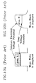
- Figure 8 is an equivalent circuit of a TFT-LCD which omits the thin film transistor connected to each liquid crystal cell. As shown, the voltage Vcom is applied to a common electrode having an internal resistance Rcom.
- C1c1 , C1c2 ... are the associated capacitances of a liquid crystal cell.
- the voltage applied to the liquid crystal cell is the difference between the common electrode voltage Vcom and the gray voltage which is applied via the thin film transistor.
- the brightness of a cell is determined based upon the voltage which is applied to the liquid crystal cell.
- the voltage potential difference between the common electrode and the gray voltage terminal of a liquid crystal cell is at a minimum and when black is displayed, the potential difference between the common electrode and the gray voltage terminal is a maximum. Therefore, the amount of electric charge in the liquid crystal cell is generally a minimum for white and a maximum for black. Accordingly, the amount of current flowing in the common electrode is generally a minimum for white and a maximum for black. Thus, the amount of current which flows in the common electrode changes based on the displayed level.
- Figure 9A is a waveform illustrating the voltage which is applied to the common electrode.
- Figure 9B is an cutput waveform of the voltage at the common electrode. As shown in Figure 9B, when white is displayed, there is generally no distortion in the common electrode voltage waveform. However, when black is displayed, distortion generally occurs in the common electrode voltage waveform. This distortion is generally attributed to the internal resistance of the panel. Due to this internal resistance, the amount of current flowing in the common electrode is greater when black is displayed, and the voltage drop difference influences the common electrode waveform.
- Figure 10A illustrates a common electrode voltage waveform which is applied to two terminals of a liquid crystal cell for white
- Figure 10B illustrates the common electrode voltage waveform for black.
- the upper potential is a common electrode voltage and the lower potential is a gray voltage potential.
- the upper potential is a common electrode voltage and the lower potential is a gray voltage.
- the areas A and B represent the total amount of charge in a liquid crystal cell.
- the common electrode voltage potential of a cell is different depending on whether white or black is displayed, due to the distortion of the common electrode voltage.
- the area A is generally different from the area B.
- the difference between the two areas can cause the difference between the gray display. Therefore, even though the same gray voltage level is applied to a liquid crystal cell, the display intensity in the cell is different based on the display in the surrounding cells.
- TFT-LCD thin film transistor-liquid crystal displays
- TFT-LCD devices and driving circuits and methods which sense a voltage drop on the common electrode and which compensate for this voltage drop.
- at least one driver signal level is provided to the plurality of drivers, wherein the at least one driver signal level is a function of the sensed voltage drop on the common electrode. Distortions in the liquid crystal cells which are caused by the voltage drop on the common electrode may thereby be reduced.
- the compensator includes a level shifter and a gray scale voltage generator.
- the level shifter is responsive to the magnitude of the sensed voltage drop on the common electrode to generate first and second voltages.
- the gray scale voltage generator is responsive to the first and second voltages, to generate more than two gray scale voltages and to apply the more than two gray scale voltages to the plurality of drivers.
- the sensor preferably includes a pad which is electrically connected to the common electrode.
- the plurality of drivers are preferably included in a driver integrated circuit.
- the driver integrated circuit preferably includes a circuit for applying a common voltage to the common electrode, and also preferably includes the sensor which senses a voltage drop on the common electrode. Accordingly, first and second pads may be connected to the common voltage electrode so that the common voltage is applied to the first pad and the sensor is connected to the second pad. If the sensor senses insufficient voltage, the voltage drop may be amplified.
- the level shifter includes a plurality of first diodes which are serially connected in a first polarity between a voltage which is complementary to a voltage which is applied to the common electrode and a voltage which is sensed on the common electrode.
- a like plurality of second diodes are also included, which are serially connected in a second polarity opposite the first polarity, between the voltage which is complementary to the voltage which is applied to the common electrode and a voltage which in sensed on the common electrode.
- a pair of reference taps tap at least a pair of intermediate nodes between the plurality of first diodes and the like plurality of second diodes.
- the gray scale voltage generator preferably comprises a plurality of resistors which are serially connected between the pair of reference taps, and a plurality of resistor taps between adjacent ones of the resistors.
- the resistor taps are used to apply the gray scale voltages to the driver.
- the generated gray scale voltages are proportional to the distorted level of the common electrode voltage.
- a constant potential may be applied to a liquid crystal cell without interference from adjacent cells.
- the generated gray voltage is thus proportional to the distorted level of the common electrode voltage, even though the common electrode voltage is distorted because of the gray voltage applied to adjacent cells.
- crosstalk may be reduced or eliminated.
- FIG. 1 is a block diagram of a thin film transistor-liquid crystal display (TFT-LCD) including driving circuits and methods according to the present invention.
- TFT-LCD thin film transistor-liquid crystal display
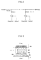
- Figure 2 is an equivalent circuit for the liquid crystal panel of Figure 1.
- Figure 3 is a plan view of a distorted signal generator of Figure 1 on a driver integrated circuit of a liquid crystal panel.
- Figure 4 is a cross-sectional view of Figure 3 taken along line A-A'.
- Figure 5 is a detailed circuit diagram of an embodiment of a level shift circuit and a gray voltage generator of Figure 1.
- Figure 6 is a waveform diagram which illustrates an embodiment of a gray voltage from the gray voltage generator of Figure 1.
- Figures 7A and 7B are waveforms illustrating a voltage which is applied to an adjacent cell when white and black, respectively, is displayed.
- Figure 8 is an equivalent circuit diagram of a conventional liquid crystal panel.
- Figures 9A and 9B are waveforms which illustrate a common electrode voltage which is applied and a distorted voltage which is produced in the circuit of Figure 8.
- Figures 10A and 10B are waveforms illustrating a voltage which is applied to an adjacent cell when white and black, respectively, is displayed in the circuit of Figure 8.
- a thin film transistor-liquid crystal display includes a liquid crystal panel 1 which includes a plurality of liquid crystal cells and a plurality of thin film transistors.
- a liquid crystal cell responds to the output voltage at the drain of a corresponding thin film transistor.
- the TFT-LCD also includes a gate driver 3 and a source driver 2 which respectively are connected to the gate terminal and the source terminal of each TFT.
- a timing circuit 4 generates a common electrode voltage Vcom.
- the timing circuit 4 also preferably generates a complementary voltage to the common electrode voltage, referred to as VcomB .
- a TFT-LCD also includes a distorted signal sensor 5 which is connected to the liquid crystal panel 1 and which senses a voltage drop on the common electrode.
- a compensator is also included, which is responsive to the sensor, to provide at least one driver signal level to the plurality of drivers.
- the at least one driver signal level is a function of the sensed voltage drop on the common electrode, to thereby reduce distortions in the liquid crystal coils which are caused by the voltage drop on the common electrode.
- the compensator includes a level shift circuit 6 and a gray voltage generator 7.
- the level shift circuit 6 receives an output signal DVcom from the distorted signal sensor 5 and the complementary common electrode voltage VcomB from the timing circuit 4, and generates gray reference voltages Va and Vb .
- the gray voltage generator 7 receives reference voltages Va and Vb and generates and outputs at least three gray voltages VG1...VG4. As shown in Figure 1, these voltages are applied to source driver 2.
- the liquid crystal panel includes a plurality of liquid crystal cells Clc1 , C1c2.. . and a plurality of thin film transistors T1, T2. ...
- a respective liquid crystal cell is connected to a respective thin film transistor.
- a liquid crystal cell and a thin film transistor are serially connected between the common electrode and a plurality of drivers.
- each liquid crystal cell includes a pair of terminals, one of which is connected to the drain of the corresponding thin film transistor and the other of which is connected to the common electrode voltage Vcom.
- the liquid crystal panel also has a panel resistance Rcom between the common electrode voltage and the liquid crystal cells. According to the invention, a distorted common electrode voltage DVcom is detected in a node between the panel resistance Rcom and the liquid crystal cells.
- the signals from gate driver 3 of Figure 1 are applied to the gate terminals of the thin film transistors labelled Gate1 , Gate2. .. in Figure 2.
- the signals from the source driver 2 are applied to the source terminals labelled Source1, Source2 ... in Figure 2.
- FIG 3 illustrates a plan view of an embodiment of a distorted signal sensor 5 of Figure 1, wherein the source distorted signal sensor 5 is incorporated into the source driver 2.
- a driver integrated circuit (driver IC) 82 is connected to a printed circuit board (PCB) 81 and the liquid crystal panel 1 using a tape automated bonding (TAB) method, where the driver IC 82 is attached to a tape carrier package (TCP) 83 .
- TCP tape carrier package
- One end of the TCP 83 is bonded to the liquid crystal panel 1 and the other end is bonded to the PCB 81 .
- the driver IC 82 may correspond to the source driver 2 of Figure 1.
- a conventional liquid crystal panel may include sixteen or more driver ICs.
- one of the dummy ports is used to apply a common electrode voltage Vcom to the liquid crystal panel.
- the other dummy port is used to detect the distorted common electrode voltage DVcom.
- one dummy port of one driving IC may be used an the distorted signal sensor 5 .
- a plurality of dummy ports may be used as the distorted signal sensor 5 .
- the dummy port of the gate driver IC which is most distant from the source driver IC is preferably used as the distorted signai sensor 5 .
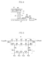
- FIG. 4 a cross-sectional view of Figure 3 taken along the line A-A' is illustrated.
- 11 is an upper substrate and 12 is a black matrix.
- Reference number 13 is an upper transparent common electrode and 14 is a silver conductive film.
- Reference number 15 is a seal and 16 is a lower substrate including a plurality of TFTs, a plurality of pixel electrodes and a plurality of conductive lines 17.
- the level shifter 6 preferably includes a plurality of first diodes D1, D2, D3, D4 and D5 which are serially connected in a first polarity between the voltage VcomB which is complementary to the voltage which is applied to the common electrode, and the voltage DVcom which is sensed on the common electrode.
- a like plurality of second diodes D6, D7, D8, D9 and D10 are serially connected in a second polarity opposite the first polarity, between voltages VcomB and DVcom.
- the diodes may be connected between the voltages via resistors R61 and R62.
- a pair of reference taps Va and Vb are provided to tap at least a pair of intermediate nodes between the plurality of first diodes and the like plurality of second diodes.
- reference voltage Va in detected between diodes D1 and D2 and between diodes D9 and D10.
- Reference voltage Vb is detected between diodes D4 and D5 and between diodes D6 and D7.
- gray voltage generator 7 includes a plurality of resistors R71-R75 which are serially connected between the pair of reference taps Va and Vb .
- a plurality of resistor taps VG1-VG4 are located between adjacent ones of the resistors.
- level shift circuit and gray voltage generator of Figure 5 generates four gray voltage levels which are applied to source driver 2. However, it will be understood that fewer or greater number of gray voltage levels may be generated.
- signals for driving a TFT of the liquid crystal panel 1 are provided from the source driver 2 and the gate driver 3.
- the timing circuit 4 provides the common electrode voltage Vcom and the complementary common electrode voltage VcomB to the common electrode of the liquid crystal panel.
- a predetermined voltage which is determined by the gate driver 3 and the source driver 2 are applied to each liquid crystal cell in a liquid crystal panel. Accordingly, each liquid crystal cell provides a display having an intensity which is proportional to the applied voltage.
- the voltage which is applied to the common electrode Vcom less the voltage drop which is produced by the panel resistance Rcom , is applied to one terminal of each liquid crystal cell.
- the drain voltage from each thin film transistor is applied to the other terminal of each liquid crystal cell.
- the source voltage is transmitted to the drain.
- the voltage applied to the source terminal of each thin film transistor is the signal from the source driver 2 and is the gray voltage for the gray scale display.
- the distorted signal sensor 5 may include an electrode pad and an amplifier.
- the electrode pad is preferably placed between an electrode where the common electrode voltage Vcom is applied and another electrode, and most preferably in a position which is most distant from the electrode where the common electrode voltage Vcom is applied.
- the amplifier may be a conventional push-pull amplifier or other conventional amplifier.
- the distorted common electrode voltage DVcom and the complementary common electrode voltage VcomB are provided to the level shift circuit 6.
- the two groups of serially connected diodes D1-D5 and D6-D10 have opposite polarities so that current can flow through only one group of serially connected diodes at a time. Which group will depend upon the voltage difference between VcomB and DVcom . For example, when VcomB is larger than DVcom , current flows only through diodes D1-D5 . Conversely, when DVcom is larger than VcomB , current flows through diodes D6 and D10 . The voltage difference between VcomB and DVcom is detected to produce the reference voltages Va and Vb. The two voltage Va and Vb are divided by the five resistors R71-R75 to produce the four gray voltages VG1-VG4 .
- the gray voltages are provided to the source driver 2.
- a switching element within the source driver 2 selects one of the four gray voltages which are provided, and the selected voltage is output to the thin film transistor on the liquid crystal panel 1 using conventional techniques.
- the waveform of the gray voltage VG1-VG4 follows that of the distorted common electrode voltage DVcom from the liquid crystal panel 1.
- the area A indicates the difference between the distorted common electrode voltage DVcom and the applied gray voltage when the adjacent liquid crystal cells display white.
- the area A of Figure 7A corresponds to the voltage which is applied to the liquid crystal cell when the adjacent liquid crystal cells display black.
- the gray voltage is proportional to the distorted level of the distorted common electrode voltage DVcom which is applied to the liquid crystal cell. Accordingly, there is little difference between the area A and the area B . It is thus possible to display the desired amount of gray because the desired amount of gray voltage is present in the liquid crystal cell regardless of the display state of adjacent liquid crystal cells. Crosstalk is thereby reduced or eliminated.
- the TFT-LCD generates a reference voltage which is proportional to the distorted level of the distorted common electrode voltage, generates the gray voltage according to the generated reference voltage and provides the source driver with the generated reference voltage.
- the common electrode voltage is distorted, the generated reference voltage can properly reflect the desired gray voltage.
- the common electrode is distorted, a constant potential difference can thus be applied to the liquid crystal cell. Crosstalk is thereby reduced or eliminated.
Landscapes
- Engineering & Computer Science (AREA)
- Chemical & Material Sciences (AREA)
- Crystallography & Structural Chemistry (AREA)
- Physics & Mathematics (AREA)
- Computer Hardware Design (AREA)
- General Physics & Mathematics (AREA)
- Theoretical Computer Science (AREA)
- Power Engineering (AREA)
- Liquid Crystal (AREA)
- Liquid Crystal Display Device Control (AREA)
- Control Of Indicators Other Than Cathode Ray Tubes (AREA)
Applications Claiming Priority (2)
| Application Number | Priority Date | Filing Date | Title |
|---|---|---|---|
| KR1019960000579A KR0163938B1 (ko) | 1996-01-13 | 1996-01-13 | 박막 트랜지스터형 액정표시장치의 구동회로 |
| KR9600579 | 1996-01-13 |
Publications (1)
| Publication Number | Publication Date |
|---|---|
| EP0784307A1 true EP0784307A1 (de) | 1997-07-16 |
Family
ID=19449371
Family Applications (1)
| Application Number | Title | Priority Date | Filing Date |
|---|---|---|---|
| EP97300149A Withdrawn EP0784307A1 (de) | 1996-01-13 | 1997-01-13 | Schaltungen und Verfahren zur Kompensation von Spannungsabfällen an gemeinsamer Elektrode für Flüssigkristallanzeige mit aktiver Matrix |
Country Status (5)
| Country | Link |
|---|---|
| US (1) | US5926157A (de) |
| EP (1) | EP0784307A1 (de) |
| JP (1) | JP4060903B2 (de) |
| KR (1) | KR0163938B1 (de) |
| TW (1) | TW335473B (de) |
Cited By (3)
| Publication number | Priority date | Publication date | Assignee | Title |
|---|---|---|---|---|
| CN101383128B (zh) * | 2007-09-07 | 2010-11-17 | 北京京东方光电科技有限公司 | 公共电极电压自动补偿的方法及装置 |
| US8189733B2 (en) | 2002-12-19 | 2012-05-29 | Semiconductor Energy Laboratory Co., Ltd. | Shift register and driving method thereof |
| CN113178176A (zh) * | 2021-04-25 | 2021-07-27 | Tcl华星光电技术有限公司 | 显示装置以及移动终端 |
Families Citing this family (33)
| Publication number | Priority date | Publication date | Assignee | Title |
|---|---|---|---|---|
| KR100516048B1 (ko) * | 1997-07-18 | 2005-12-09 | 삼성전자주식회사 | 크로스토크를감소시키기위한계조전압발생회로및이를이용한액정표시장치 |
| KR100448940B1 (ko) * | 1997-07-25 | 2004-11-26 | 삼성전자주식회사 | 박막 트랜지스터 액정 표시 장치의 구동 장치 |
| KR100251543B1 (ko) * | 1997-07-28 | 2000-04-15 | 구본준 | 계조보정용 전압공급장치 |
| DE19808982A1 (de) * | 1998-03-03 | 1999-09-09 | Siemens Ag | Aktivmatrix-Flüssigkristallanzeige |
| TW490580B (en) * | 1998-11-13 | 2002-06-11 | Hitachi Ltd | Liquid crystal display apparatus and its drive method |
| TW523622B (en) * | 1998-12-24 | 2003-03-11 | Samsung Electronics Co Ltd | Liquid crystal display |
| KR20000074515A (ko) * | 1999-05-21 | 2000-12-15 | 윤종용 | 액정표시장치 및 그의 화상 신호 전송 배선 형성 방법 |
| US6985128B1 (en) * | 2000-07-31 | 2006-01-10 | Sony Corporation | Liquid crystal display panel and production method of the same, and liquid crystal display apparatus |
| KR100806906B1 (ko) * | 2001-09-25 | 2008-02-22 | 삼성전자주식회사 | 액정 표시 장치와 이의 구동 장치 및 구동 방법 |
| KR100806903B1 (ko) * | 2001-09-27 | 2008-02-22 | 삼성전자주식회사 | 액정 표시 장치 및 이의 구동 방법 |
| JP3854905B2 (ja) * | 2002-07-30 | 2006-12-06 | 株式会社 日立ディスプレイズ | 液晶表示装置 |
| KR100920378B1 (ko) * | 2002-11-01 | 2009-10-07 | 엘지디스플레이 주식회사 | 액정표시장치 |
| KR100864501B1 (ko) * | 2002-11-19 | 2008-10-20 | 삼성전자주식회사 | 액정 표시 장치 |
| KR101030694B1 (ko) * | 2004-02-19 | 2011-04-26 | 삼성전자주식회사 | 액정표시패널 및 이를 갖는 액정표시장치 |
| KR101056374B1 (ko) * | 2004-02-20 | 2011-08-11 | 삼성전자주식회사 | 펄스 보상기, 이를 갖는 영상표시장치 및 영상표시장치의구동방법 |
| CN100458906C (zh) | 2004-02-20 | 2009-02-04 | 三星电子株式会社 | 脉冲补偿器、显示装置及驱动该显示装置的方法 |
| TWI280555B (en) * | 2004-12-17 | 2007-05-01 | Au Optronics Corp | Liquid crystal display and driving method |
| CN100489604C (zh) * | 2004-12-30 | 2009-05-20 | 友达光电股份有限公司 | 液晶显示器及其显示方法 |
| TW200729139A (en) * | 2006-01-16 | 2007-08-01 | Au Optronics Corp | Driving method capable improving display uniformity |
| TWI345093B (en) * | 2006-11-10 | 2011-07-11 | Chimei Innolux Corp | Method of manufacturing liquid crystal display |
| TWI469129B (zh) | 2008-04-18 | 2015-01-11 | Innolux Corp | 液晶顯示裝置公共電壓調整方法 |
| KR101330353B1 (ko) * | 2008-08-08 | 2013-11-20 | 엘지디스플레이 주식회사 | 액정표시장치와 그 구동방법 |
| TWI406247B (zh) * | 2009-05-04 | 2013-08-21 | Au Optronics Corp | 用於液晶顯示裝置之共用電壓補償電路與補償方法 |
| TWI425467B (zh) * | 2010-02-03 | 2014-02-01 | Au Optronics Corp | 具有抑制共用電壓之漣波的顯示器 |
| TWI441153B (zh) * | 2011-08-11 | 2014-06-11 | 瀚宇彩晶股份有限公司 | 顯示裝置及其伽瑪電壓產生器 |
| US20130093798A1 (en) * | 2011-10-12 | 2013-04-18 | Shenzhen China Star Optoelectronics Technology Co., Ltd. | Liquid crystal display device and signal driving method for the same |
| CN103065594B (zh) * | 2012-12-14 | 2017-04-12 | 深圳市华星光电技术有限公司 | 一种数据驱动电路、液晶显示装置及一种驱动方法 |
| US9135882B2 (en) | 2012-12-14 | 2015-09-15 | Shenzhen China Star Optoelectronics Technology Co., Ltd | Data driver circuit having compensation module, LCD device and driving method |
| US9761188B2 (en) * | 2015-03-06 | 2017-09-12 | Apple Inc. | Content-based VCOM driving |
| CN104795036B (zh) * | 2015-04-28 | 2018-02-27 | 京东方科技集团股份有限公司 | 一种补偿电路、驱动电路及其工作方法、显示装置 |
| CN104882104B (zh) * | 2015-05-11 | 2017-05-31 | 深圳市华星光电技术有限公司 | 一种液晶显示面板及装置 |
| CN105096855B (zh) * | 2015-07-22 | 2018-11-06 | 深圳市华星光电技术有限公司 | 液晶面板公共电压调整装置及液晶面板公共电压调整方法 |
| CN114913826A (zh) * | 2022-05-16 | 2022-08-16 | 星源电子科技(深圳)有限公司 | 一种低串扰的液晶模组的制作方法 |
Citations (3)
| Publication number | Priority date | Publication date | Assignee | Title |
|---|---|---|---|---|
| DE3314778A1 (de) * | 1982-04-26 | 1983-11-10 | Japan Electronic Industry Development Association, Tokyo | Fluessigkristall-anzeigevorrichtung und methode zu ihrem betrieb |
| EP0455204A2 (de) * | 1990-05-01 | 1991-11-06 | Stanley Electric Co., Ltd. | Spannungsversorgung für eine Flüssigkristall-Punktmatrixanzeige |
| EP0606763A1 (de) * | 1992-12-28 | 1994-07-20 | Sharp Kabushiki Kaisha | Treiberschaltung für gemeinsame Elektrode zur Verwendung in einem Anzeigegerät |
Family Cites Families (6)
| Publication number | Priority date | Publication date | Assignee | Title |
|---|---|---|---|---|
| US4921334A (en) * | 1988-07-18 | 1990-05-01 | General Electric Company | Matrix liquid crystal display with extended gray scale |
| US5008657A (en) * | 1989-01-31 | 1991-04-16 | Varo, Inc. | Self adjusting matrix display |
| JPH06180564A (ja) * | 1992-05-14 | 1994-06-28 | Toshiba Corp | 液晶表示装置 |
| SG49735A1 (en) * | 1993-04-05 | 1998-06-15 | Cirrus Logic Inc | System for compensating crosstalk in LCDS |
| JP3346652B2 (ja) * | 1993-07-06 | 2002-11-18 | シャープ株式会社 | 電圧補償回路および表示装置 |
| US5625373A (en) * | 1994-07-14 | 1997-04-29 | Honeywell Inc. | Flat panel convergence circuit |
-
1996
- 1996-01-13 KR KR1019960000579A patent/KR0163938B1/ko not_active Expired - Lifetime
-
1997
- 1997-01-10 JP JP00331597A patent/JP4060903B2/ja not_active Expired - Lifetime
- 1997-01-13 US US08/782,399 patent/US5926157A/en not_active Expired - Lifetime
- 1997-01-13 EP EP97300149A patent/EP0784307A1/de not_active Withdrawn
- 1997-01-16 TW TW086100408A patent/TW335473B/zh not_active IP Right Cessation
Patent Citations (3)
| Publication number | Priority date | Publication date | Assignee | Title |
|---|---|---|---|---|
| DE3314778A1 (de) * | 1982-04-26 | 1983-11-10 | Japan Electronic Industry Development Association, Tokyo | Fluessigkristall-anzeigevorrichtung und methode zu ihrem betrieb |
| EP0455204A2 (de) * | 1990-05-01 | 1991-11-06 | Stanley Electric Co., Ltd. | Spannungsversorgung für eine Flüssigkristall-Punktmatrixanzeige |
| EP0606763A1 (de) * | 1992-12-28 | 1994-07-20 | Sharp Kabushiki Kaisha | Treiberschaltung für gemeinsame Elektrode zur Verwendung in einem Anzeigegerät |
Cited By (5)
| Publication number | Priority date | Publication date | Assignee | Title |
|---|---|---|---|---|
| US8189733B2 (en) | 2002-12-19 | 2012-05-29 | Semiconductor Energy Laboratory Co., Ltd. | Shift register and driving method thereof |
| US8526568B2 (en) | 2002-12-19 | 2013-09-03 | Semiconductor Energy Laboratory Co., Ltd. | Shift register and driving method thereof |
| CN101383128B (zh) * | 2007-09-07 | 2010-11-17 | 北京京东方光电科技有限公司 | 公共电极电压自动补偿的方法及装置 |
| CN113178176A (zh) * | 2021-04-25 | 2021-07-27 | Tcl华星光电技术有限公司 | 显示装置以及移动终端 |
| CN113178176B (zh) * | 2021-04-25 | 2023-11-28 | Tcl华星光电技术有限公司 | 显示装置以及移动终端 |
Also Published As
| Publication number | Publication date |
|---|---|
| KR0163938B1 (ko) | 1999-03-20 |
| JP4060903B2 (ja) | 2008-03-12 |
| JPH09265279A (ja) | 1997-10-07 |
| TW335473B (en) | 1998-07-01 |
| US5926157A (en) | 1999-07-20 |
| KR970060028A (ko) | 1997-08-12 |
Similar Documents
| Publication | Publication Date | Title |
|---|---|---|
| US5926157A (en) | Voltage drop compensating driving circuits and methods for liquid crystal displays | |
| US7224353B2 (en) | Liquid crystal display device and driving method thereof | |
| KR100874637B1 (ko) | 라인 온 글래스형 액정표시장치 | |
| US7705820B2 (en) | Liquid crystal display of line-on-glass type | |
| JPH09265279A5 (de) | ||
| KR100933447B1 (ko) | 액정 표시 패널의 게이트 구동 방법 및 장치 | |
| US7463324B2 (en) | Liquid crystal display panel of line on glass type | |
| US20060001643A1 (en) | Liquid crystal display and driving method thereof | |
| US20040263447A1 (en) | Method and apparatus for driving liquid crystal display panel | |
| KR100922789B1 (ko) | 라인 온 글래스형 액정 표시 장치 및 그 구동방법 | |
| KR100904264B1 (ko) | 액정표시장치 | |
| KR100898792B1 (ko) | 액정표시장치 | |
| KR100861273B1 (ko) | 라인 온 글래스형 액정표시장치 | |
| KR101010129B1 (ko) | 액정표시장치 | |
| KR101002306B1 (ko) | 라인 온 글래스형 액정 표시 장치 | |
| KR20060018396A (ko) | 액정 표시 장치 | |
| KR20070052148A (ko) | 액정 표시 장치 및 이의 구동 방법 | |
| KR20040022939A (ko) | 액정표시장치 | |
| KR20040055189A (ko) | 액정표시장치 | |
| KR20050047673A (ko) | 라인 온 글래스형 액정 표시 장치 및 그 구동방법 |
Legal Events
| Date | Code | Title | Description |
|---|---|---|---|
| PUAI | Public reference made under article 153(3) epc to a published international application that has entered the european phase |
Free format text: ORIGINAL CODE: 0009012 |
|
| AK | Designated contracting states |
Kind code of ref document: A1 Designated state(s): DE FR GB |
|
| 17P | Request for examination filed |
Effective date: 19971126 |
|
| 17Q | First examination report despatched |
Effective date: 20011029 |
|
| 17Q | First examination report despatched |
Effective date: 20011029 |
|
| RAP1 | Party data changed (applicant data changed or rights of an application transferred) |
Owner name: SAMSUNG ELECTRONICS CO., LTD. |
|
| STAA | Information on the status of an ep patent application or granted ep patent |
Free format text: STATUS: THE APPLICATION IS DEEMED TO BE WITHDRAWN |
|
| 18D | Application deemed to be withdrawn |
Effective date: 20130813 |