EP0784363B1 - Laser à émission de surface à cavité verticale et son procédé de fabrication - Google Patents
Laser à émission de surface à cavité verticale et son procédé de fabrication Download PDFInfo
- Publication number
- EP0784363B1 EP0784363B1 EP96309451A EP96309451A EP0784363B1 EP 0784363 B1 EP0784363 B1 EP 0784363B1 EP 96309451 A EP96309451 A EP 96309451A EP 96309451 A EP96309451 A EP 96309451A EP 0784363 B1 EP0784363 B1 EP 0784363B1
- Authority
- EP
- European Patent Office
- Prior art keywords
- layer
- layered film
- layers
- semiconductor multi
- semiconductor
- Prior art date
- Legal status (The legal status is an assumption and is not a legal conclusion. Google has not performed a legal analysis and makes no representation as to the accuracy of the status listed.)
- Expired - Lifetime
Links
Images








Classifications
-
- H—ELECTRICITY
- H01—ELECTRIC ELEMENTS
- H01S—DEVICES USING THE PROCESS OF LIGHT AMPLIFICATION BY STIMULATED EMISSION OF RADIATION [LASER] TO AMPLIFY OR GENERATE LIGHT; DEVICES USING STIMULATED EMISSION OF ELECTROMAGNETIC RADIATION IN WAVE RANGES OTHER THAN OPTICAL
- H01S5/00—Semiconductor lasers
- H01S5/10—Construction or shape of the optical resonator, e.g. extended or external cavity, coupled cavities, bent-guide, varying width, thickness or composition of the active region
- H01S5/18—Surface-emitting [SE] lasers, e.g. having both horizontal and vertical cavities
- H01S5/183—Surface-emitting [SE] lasers, e.g. having both horizontal and vertical cavities having only vertical cavities, e.g. vertical cavity surface-emitting lasers [VCSEL]
- H01S5/18361—Structure of the reflectors, e.g. hybrid mirrors
- H01S5/1838—Reflector bonded by wafer fusion or by an intermediate compound
-
- B—PERFORMING OPERATIONS; TRANSPORTING
- B82—NANOTECHNOLOGY
- B82Y—SPECIFIC USES OR APPLICATIONS OF NANOSTRUCTURES; MEASUREMENT OR ANALYSIS OF NANOSTRUCTURES; MANUFACTURE OR TREATMENT OF NANOSTRUCTURES
- B82Y20/00—Nanooptics, e.g. quantum optics or photonic crystals
-
- H—ELECTRICITY
- H01—ELECTRIC ELEMENTS
- H01S—DEVICES USING THE PROCESS OF LIGHT AMPLIFICATION BY STIMULATED EMISSION OF RADIATION [LASER] TO AMPLIFY OR GENERATE LIGHT; DEVICES USING STIMULATED EMISSION OF ELECTROMAGNETIC RADIATION IN WAVE RANGES OTHER THAN OPTICAL
- H01S5/00—Semiconductor lasers
- H01S5/10—Construction or shape of the optical resonator, e.g. extended or external cavity, coupled cavities, bent-guide, varying width, thickness or composition of the active region
- H01S5/18—Surface-emitting [SE] lasers, e.g. having both horizontal and vertical cavities
- H01S5/183—Surface-emitting [SE] lasers, e.g. having both horizontal and vertical cavities having only vertical cavities, e.g. vertical cavity surface-emitting lasers [VCSEL]
- H01S5/18308—Surface-emitting [SE] lasers, e.g. having both horizontal and vertical cavities having only vertical cavities, e.g. vertical cavity surface-emitting lasers [VCSEL] having a special structure for lateral current or light confinement
-
- H—ELECTRICITY
- H01—ELECTRIC ELEMENTS
- H01S—DEVICES USING THE PROCESS OF LIGHT AMPLIFICATION BY STIMULATED EMISSION OF RADIATION [LASER] TO AMPLIFY OR GENERATE LIGHT; DEVICES USING STIMULATED EMISSION OF ELECTROMAGNETIC RADIATION IN WAVE RANGES OTHER THAN OPTICAL
- H01S2301/00—Functional characteristics
- H01S2301/17—Semiconductor lasers comprising special layers
- H01S2301/176—Specific passivation layers on surfaces other than the emission facet
-
- H—ELECTRICITY
- H01—ELECTRIC ELEMENTS
- H01S—DEVICES USING THE PROCESS OF LIGHT AMPLIFICATION BY STIMULATED EMISSION OF RADIATION [LASER] TO AMPLIFY OR GENERATE LIGHT; DEVICES USING STIMULATED EMISSION OF ELECTROMAGNETIC RADIATION IN WAVE RANGES OTHER THAN OPTICAL
- H01S5/00—Semiconductor lasers
- H01S5/10—Construction or shape of the optical resonator, e.g. extended or external cavity, coupled cavities, bent-guide, varying width, thickness or composition of the active region
- H01S5/18—Surface-emitting [SE] lasers, e.g. having both horizontal and vertical cavities
- H01S5/183—Surface-emitting [SE] lasers, e.g. having both horizontal and vertical cavities having only vertical cavities, e.g. vertical cavity surface-emitting lasers [VCSEL]
- H01S5/18305—Surface-emitting [SE] lasers, e.g. having both horizontal and vertical cavities having only vertical cavities, e.g. vertical cavity surface-emitting lasers [VCSEL] with emission through the substrate, i.e. bottom emission
-
- H—ELECTRICITY
- H01—ELECTRIC ELEMENTS
- H01S—DEVICES USING THE PROCESS OF LIGHT AMPLIFICATION BY STIMULATED EMISSION OF RADIATION [LASER] TO AMPLIFY OR GENERATE LIGHT; DEVICES USING STIMULATED EMISSION OF ELECTROMAGNETIC RADIATION IN WAVE RANGES OTHER THAN OPTICAL
- H01S5/00—Semiconductor lasers
- H01S5/10—Construction or shape of the optical resonator, e.g. extended or external cavity, coupled cavities, bent-guide, varying width, thickness or composition of the active region
- H01S5/18—Surface-emitting [SE] lasers, e.g. having both horizontal and vertical cavities
- H01S5/183—Surface-emitting [SE] lasers, e.g. having both horizontal and vertical cavities having only vertical cavities, e.g. vertical cavity surface-emitting lasers [VCSEL]
- H01S5/18308—Surface-emitting [SE] lasers, e.g. having both horizontal and vertical cavities having only vertical cavities, e.g. vertical cavity surface-emitting lasers [VCSEL] having a special structure for lateral current or light confinement
- H01S5/18311—Surface-emitting [SE] lasers, e.g. having both horizontal and vertical cavities having only vertical cavities, e.g. vertical cavity surface-emitting lasers [VCSEL] having a special structure for lateral current or light confinement using selective oxidation
-
- H—ELECTRICITY
- H01—ELECTRIC ELEMENTS
- H01S—DEVICES USING THE PROCESS OF LIGHT AMPLIFICATION BY STIMULATED EMISSION OF RADIATION [LASER] TO AMPLIFY OR GENERATE LIGHT; DEVICES USING STIMULATED EMISSION OF ELECTROMAGNETIC RADIATION IN WAVE RANGES OTHER THAN OPTICAL
- H01S5/00—Semiconductor lasers
- H01S5/10—Construction or shape of the optical resonator, e.g. extended or external cavity, coupled cavities, bent-guide, varying width, thickness or composition of the active region
- H01S5/18—Surface-emitting [SE] lasers, e.g. having both horizontal and vertical cavities
- H01S5/183—Surface-emitting [SE] lasers, e.g. having both horizontal and vertical cavities having only vertical cavities, e.g. vertical cavity surface-emitting lasers [VCSEL]
- H01S5/18308—Surface-emitting [SE] lasers, e.g. having both horizontal and vertical cavities having only vertical cavities, e.g. vertical cavity surface-emitting lasers [VCSEL] having a special structure for lateral current or light confinement
- H01S5/18322—Position of the structure
- H01S5/1833—Position of the structure with more than one structure
-
- H—ELECTRICITY
- H01—ELECTRIC ELEMENTS
- H01S—DEVICES USING THE PROCESS OF LIGHT AMPLIFICATION BY STIMULATED EMISSION OF RADIATION [LASER] TO AMPLIFY OR GENERATE LIGHT; DEVICES USING STIMULATED EMISSION OF ELECTROMAGNETIC RADIATION IN WAVE RANGES OTHER THAN OPTICAL
- H01S5/00—Semiconductor lasers
- H01S5/20—Structure or shape of the semiconductor body to guide the optical wave ; Confining structures perpendicular to the optical axis, e.g. index or gain guiding, stripe geometry, broad area lasers, gain tailoring, transverse or lateral reflectors, special cladding structures, MQW barrier reflection layers
- H01S5/2054—Methods of obtaining the confinement
- H01S5/2059—Methods of obtaining the confinement by means of particular conductivity zones, e.g. obtained by particle bombardment or diffusion
- H01S5/2063—Methods of obtaining the confinement by means of particular conductivity zones, e.g. obtained by particle bombardment or diffusion obtained by particle bombardment
-
- H—ELECTRICITY
- H01—ELECTRIC ELEMENTS
- H01S—DEVICES USING THE PROCESS OF LIGHT AMPLIFICATION BY STIMULATED EMISSION OF RADIATION [LASER] TO AMPLIFY OR GENERATE LIGHT; DEVICES USING STIMULATED EMISSION OF ELECTROMAGNETIC RADIATION IN WAVE RANGES OTHER THAN OPTICAL
- H01S5/00—Semiconductor lasers
- H01S5/20—Structure or shape of the semiconductor body to guide the optical wave ; Confining structures perpendicular to the optical axis, e.g. index or gain guiding, stripe geometry, broad area lasers, gain tailoring, transverse or lateral reflectors, special cladding structures, MQW barrier reflection layers
- H01S5/22—Structure or shape of the semiconductor body to guide the optical wave ; Confining structures perpendicular to the optical axis, e.g. index or gain guiding, stripe geometry, broad area lasers, gain tailoring, transverse or lateral reflectors, special cladding structures, MQW barrier reflection layers having a ridge or stripe structure
- H01S5/2205—Structure or shape of the semiconductor body to guide the optical wave ; Confining structures perpendicular to the optical axis, e.g. index or gain guiding, stripe geometry, broad area lasers, gain tailoring, transverse or lateral reflectors, special cladding structures, MQW barrier reflection layers having a ridge or stripe structure comprising special burying or current confinement layers
- H01S5/2222—Structure or shape of the semiconductor body to guide the optical wave ; Confining structures perpendicular to the optical axis, e.g. index or gain guiding, stripe geometry, broad area lasers, gain tailoring, transverse or lateral reflectors, special cladding structures, MQW barrier reflection layers having a ridge or stripe structure comprising special burying or current confinement layers having special electric properties
- H01S5/2224—Structure or shape of the semiconductor body to guide the optical wave ; Confining structures perpendicular to the optical axis, e.g. index or gain guiding, stripe geometry, broad area lasers, gain tailoring, transverse or lateral reflectors, special cladding structures, MQW barrier reflection layers having a ridge or stripe structure comprising special burying or current confinement layers having special electric properties semi-insulating semiconductors
-
- H—ELECTRICITY
- H01—ELECTRIC ELEMENTS
- H01S—DEVICES USING THE PROCESS OF LIGHT AMPLIFICATION BY STIMULATED EMISSION OF RADIATION [LASER] TO AMPLIFY OR GENERATE LIGHT; DEVICES USING STIMULATED EMISSION OF ELECTROMAGNETIC RADIATION IN WAVE RANGES OTHER THAN OPTICAL
- H01S5/00—Semiconductor lasers
- H01S5/30—Structure or shape of the active region; Materials used for the active region
- H01S5/34—Structure or shape of the active region; Materials used for the active region comprising quantum well or superlattice structures, e.g. single quantum well [SQW] lasers, multiple quantum well [MQW] lasers or graded index separate confinement heterostructure [GRINSCH] lasers
- H01S5/343—Structure or shape of the active region; Materials used for the active region comprising quantum well or superlattice structures, e.g. single quantum well [SQW] lasers, multiple quantum well [MQW] lasers or graded index separate confinement heterostructure [GRINSCH] lasers in AIIIBV compounds, e.g. AlGaAs-laser, InP-based laser
- H01S5/34306—Structure or shape of the active region; Materials used for the active region comprising quantum well or superlattice structures, e.g. single quantum well [SQW] lasers, multiple quantum well [MQW] lasers or graded index separate confinement heterostructure [GRINSCH] lasers in AIIIBV compounds, e.g. AlGaAs-laser, InP-based laser emitting light at a wavelength longer than 1000nm, e.g. InP based 1300 and 1500nm lasers
-
- H—ELECTRICITY
- H01—ELECTRIC ELEMENTS
- H01S—DEVICES USING THE PROCESS OF LIGHT AMPLIFICATION BY STIMULATED EMISSION OF RADIATION [LASER] TO AMPLIFY OR GENERATE LIGHT; DEVICES USING STIMULATED EMISSION OF ELECTROMAGNETIC RADIATION IN WAVE RANGES OTHER THAN OPTICAL
- H01S5/00—Semiconductor lasers
- H01S5/30—Structure or shape of the active region; Materials used for the active region
- H01S5/34—Structure or shape of the active region; Materials used for the active region comprising quantum well or superlattice structures, e.g. single quantum well [SQW] lasers, multiple quantum well [MQW] lasers or graded index separate confinement heterostructure [GRINSCH] lasers
- H01S5/343—Structure or shape of the active region; Materials used for the active region comprising quantum well or superlattice structures, e.g. single quantum well [SQW] lasers, multiple quantum well [MQW] lasers or graded index separate confinement heterostructure [GRINSCH] lasers in AIIIBV compounds, e.g. AlGaAs-laser, InP-based laser
- H01S5/3434—Structure or shape of the active region; Materials used for the active region comprising quantum well or superlattice structures, e.g. single quantum well [SQW] lasers, multiple quantum well [MQW] lasers or graded index separate confinement heterostructure [GRINSCH] lasers in AIIIBV compounds, e.g. AlGaAs-laser, InP-based laser with a well layer comprising at least both As and P as V-compounds
Definitions
- the present invention relates to a surface emitting semiconductor laser and a method of manufacturing the same. Especially the present invention relates to a vertical-cavity surface-emitting semiconductor laser for long wavelengths (i.e., 1.3 to 1.55 ⁇ m) to be used as an optical source for a system of optical communication, optical interconnection, optical data-processing, or the like, in the field of optical data-communication or optical data-processing, and also to a method of manufacturing the novel vertical-cavity surface-emitting semiconductor lasers for long wavelengths.
- a vertical-cavity surface-emitting semiconductor laser for long wavelengths i.e., 1.3 to 1.55 ⁇ m
- the vertical-cavity surface-emitting lasers have been investigated and developed as optical sources to be applied in the fields of optical-signal processing, optical-data processing, and so on because of their feasibility of two dimensional high-integration. That is, each of them comprises reflection layers consisting of semiconductor multi-layered films, respectively, and emits light at long wavelengths of 1 to 2 ⁇ m that correspond to low-loss wavelengths of a quartz-crystal fiber.
- VCSELs vertical-cavity surface-emitting lasers
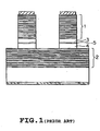
- Fig. 1 there is shown one of examples of the conventional long-wavelength VCSELs as described in D. I Babic et al. Appl. Phys. Lett., vol. 66 (69), 1030-1032 (1995).
- the VCSEL comprises: AlAs/GaAs reflection layers (mirrors) 1, 2 consisting of a plurality of AlAs layers and a plurality of GaAs layers, which are alternatively piled one by one into a stack; and an emission region consisting of InP cladding layers 3, 4 and an active layer 5 positioned between the cladding layers 3, 4.
- the emission region is sandwiched between the mirrors 1, 2 and they are directly fused together. That is, the InP cladding layers 3, 4 on both sides of the active layer 5 are directly fused to the AlAs/GaAs mirrors 1, 2, respectively.
- a substantially small difference among refractive indexes of semiconductor layers (e.g., InP and InGaAs) of a reflection layer can be observed when the reflection layer is formed using the InP related semiconductor that emits light at a long wavelength, resulting in the difficulty of obtaining a sufficient degree of reflection. Therefore it is necessary to use another reflection layer, for example one made of AlGaAs/GaAs, with a large difference between the refractive indexes of its constituent layers. However it is difficult to grow the InP semiconductor layer on a GaAs semiconductor (or vice versa). Even if the crystal growth is attained, a crystal defect such as a dislocation extends to a long distance from a growth interface into a growing film.
- semiconductor layers e.g., InP and InGaAs
- a crystal defect generated on the interface of the fused layers extends in parallel with the interface without entering into the fused layers, so that it reduces the tendency to introduce the crystal defect into the layers. Therefore, a person skilled in the art uses a structure prepared by forming an emission region using the InP semiconductor and fusing it with a highly-reflective GaAs reflection layer.
- the conventional VCSEL having the above problems is not a suitable light source of any one of the systems such as optical interconnection and optical data-processing systems that use a low threshold current (i.e., a low power consumption) and optical communication systems that require a precisely-controlled long wavelength.
- a low threshold current i.e., a low power consumption
- optical communication systems that require a precisely-controlled long wavelength.
- VCSEL vertical-cavity surface-emitting laser
- fabrication method in which the optical loss due to e.g. the cladding layers 3, 4 does not increase even if the distance between the fused interface and the active layer 5 is comparatively extended. It is intended that the distance between the fused interface and the active layer 5 can be properly extended, so that there is no possibility of extending a crystal defect to be caused in the fused interface to the active layer.
- a VCSEL with a low threshold can be prepared because of a small effective cavity length, which results in low optical loss.
- VCSEL vertical-cavity surface-emitting laser
- a vertical-cavity surface-emitting semiconductor laser comprising:
- the first semiconductor multi-layered film may further comprise a plurality of Al x10 Ga 1-x10 As layers (0 ⁇ x10 ⁇ 1) in a manner that each Al x10 Ga 1-x10 As layer is thinner than the Al x1 Ga 1-x1 As layer and the Al x2 Ga 1-x2 As layer and is provided between the Al x1 Ga 1-x1 As layer and the Al x2 Ga 1-x2 As layer.
- the fourth semiconductor multi-layered film may further comprise a plurality of Al x11 Ga 1-x11 As layers (0 ⁇ x11 ⁇ 1) in a manner that each Al x11 Ga 1-x11 As layer is thinner than the Al x8 Ga 1-x8 As layer and the Al x9 Ga 1-x9 As layer and is provided between the Al x8 Ga 1-x8 As layer and the Al x9 Ga 1-x9 As layer.
- the second semiconductor multi-layered film may comprise at least one high-resistance portion as an insulation layer formed by an ion-injection.
- Each of the second semiconductor multi-layered film and the third semiconductor multi-layered film may comprise a conductive portion as a conductive layer formed by an ion-injection.
- a vertical-cavity surface-emitting semiconductor laser may further comprise:
- a vertical-cavity surface-emitting semiconductor laser may further comprise at least one layer selected from a group of:
- a vertical-cavity surface-emitting semiconductor laser may further comprise at least one layer selected from a group of:
- a vertical-cavity surface-emitting semiconductor laser comprising:
- the active layer may have a multiple-quantum-well structure.
- a vertical-cavity surface-emitting semiconductor laser comprising the steps of:
- the step of growing the first semiconductor multi-layered film on the GaAs substrate may further include a step of forming an Al x10 Ga 1-x10 As layer (0 ⁇ x10 ⁇ 1) between the Al x1 Ga 1-x1 As layer and the Al x2 Ga 1-x2 As layer, in which the Al x10 Ga 1-x10 As layer is thinner than the Al x1 Ga 1-x1 As layer and the Al x2 Ga 1-x2 As layer.
- the step of growing the fourth semiconductor multi-layered film on the second GaAs substrate may further include a step of forming a Al x11 Ga 1-x11 As layer (0 ⁇ x11 ⁇ 1) between the Al x8 Ga 1-x8 As layer and the Al x8 Ga 1-x8 As layer, in which the Al x11 Ga 1-x11 As layer is thinner than the Al x8 Ga 1-x8 As layer and the Al x8 Ga 1-x8 As layer.
- At least one high-resistance portion as an insulation layer may be formed in at least one of either the second semiconductor multi-layered film or the third semiconductor multi-layered film by ion-injection.
- At least one conductive portion as a conductive layer may be formed in each of the second semiconductor multi-layered film and the third semiconductor multi-layered film by ion-injection.
- a mesa structure may be formed by etching down from the fourth semiconductor multi-layered film to a predetermined point of the second semiconductor multi-layered film; and a buried hetero-structure is formed on the mesa structure by growing a semiconductor selected from a group of InP and other semiconductors that have lattice constants matching with that of InP.
- a first In x12 Al x13 Ga 1-x12-x13 As layer (0 ⁇ x12, x13 ⁇ 1) may be formed between the second semiconductor multi-layered film and the active layer and a second In x12 Al x13 Ga 1-x12-x13 As layer (0 ⁇ x12, x13 ⁇ 1) is formed between the third semiconductor multi-layered film and the active layer, and after forming a mesa structure, an oxidized portion is formed in the first and second In x12 Al x13 Ga 1-x12-x13 As layers.
- a cladding layer consisting of In x14 Ga 1-x14 As 1-y14 P 1-y14 (0 ⁇ x14, y 14 ⁇ 1) may be formed at at least one of either the interface between the active layer and the second semiconductor multi-layered film and the interface between the active layer and the third semiconductor multi-layered film.
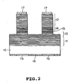
- Fig. 2 is a schematic sectional view of one of the preferred embodiments of the vertical-cavity surface-emitting lasers (VCSELs) in accordance with the present invention.
- VCSELs vertical-cavity surface-emitting lasers
- a VCSEL consists of a plurality of stacked layers on a GaAs substrate 16.
- electrodes 18 and anti-reflection (AR) films 19 are provided on one surface (i.e., a bottom surface) of the GaAs substrate 16, while on the other side thereof there are stacked a first semiconductor layer (an AlGaAs/AlGaAs reflection layer) 11, a second semiconductor layer (an InGaAsP/InGaAsP reflection layer) 13, an active layer 15, a third semiconductor layer (InGaAsP/InGaAsP reflection layer)14, and a fourth semiconductor layer (AlAs/AlGaAs reflection layer)12 in that order.
- a mesa structure is formed by etching down an upper surface of the top layer (i.e., the AlGaAs/AlGaAs reflection layer 12) to a certain point of the InGaAsP/InGaAsP reflection layer 13.
- electrodes 17 are provided on the upper surface of the AlGaAs/AlGaAs reflection layer 12.
- an emission region is constructed of the InGaAsP/InGaAsP reflection layers 13, 14 and the active layer 15.
- These layers 13, 14, 15 can be grown on the InP substrate, so that a fusion-interface can be formed between the InGaAsP/InGaAsP reflection layers 13 and the AlGaAs/AlGaAs reflection layer 11, and also another fusion-interface can be formed between the InGaAP/InGaAsP reflection layer 14 and the AlGaAs/AlGaAs reflection layer 12.
- the active layer 15 can be grown on the same substrate together with the InGaAsP/InGaAsP reflection layers 13, 14, so that it allows a measurement of oscillation wavelength before fusing the emission region with the substrate having the AlGaAs/AlGaAs reflection layer 11 or 12 thereon.
- the InGaAsP/InGaAsP reflection layer hardly attains the reflective index of 99% or more, the resonant modes can be determined at the time of after forming the InGaAsP/InGaAsP reflection layers on the top and bottom sides of the active layer 15, respectively.
- the InGaAsP/InGaAsP reflection layer 13 under the active layer 15 is provided, so that it becomes possible to increase an acceptable depth of etching at the time of forming the buried hetero-structure and also it can be performed in conjunction with a selectable chemical etching.
- the etching depth can be easily regulated uniformly and it becomes possible to increase the yields at the time of forming the buried hetero-structure, dramatically.
- reflection layers are described as multi-layers made from InGaAsP or AlGaAs.
- the InGaAsP/InGaAsP reflection layer does not mean not only multi-layer made from quarternary alloys but also that made from InGaAsP and InP.
- AlGaAs/AlGaAs reflection layer does not mean not only multi-layer made from ternary alloys but also that made from AlAs and GaAs.
- Figs. 3A to 3C are cross-sectional views of three epitaxial structures and Figs. 4A and 4B are cross-sectional views of wafer-fused structure for explaining the process for manufacturing the VCSEL of the present embodiment.
- n-AlAs layers and n-GaAs layers are epitaxially grown in alternating manner on the n-type GaAs substrate 30 to make 27 pairs thereof as a n-type AlAs/GaAs reflection layer 31 in which each layer has a thickness corresponding to a quarter of 1.55 ⁇ m optical length.
- a p-type InGaAsP/InP reflection layer 33 is formed on a p-type InP substrate 35 by an epitaxial growing P-InGaAsP layers and P-InP layers to make 10 pairs thereof, in which each layer has a thickness corresponding to a quarter of 1.55 ⁇ m optical length.
- an InGaAsP (bulk) active layer 34 is epitaxially formed as one having a thickness corresponding to 1.55 ⁇ m optical length, followed by epitaxially forming an n-type InGaAsP/InP reflection layer 32 using n-InGaAsP layers and n-InP layers in alternating manner as 10.5 pairs thereof, in which each layer has a thickness corresponding to a quarter of 1.55 ⁇ m optical length.
- a surface of the epitaxially layered structure on the GaAs substrate 30 is treated with a solution of HF, while a surface of the epitaxially layered structure on the InP substrate 35 is treated with solutions of H 2 SO 4 :H 2 O 2 :H 2 O (3:1:1) and HF, for removing naturally-oxidized films on their surfaces.
- the former surface is brought into intimate contact with the latter surface and loaded in a hydrogen atmosphere, followed by an annealing around 600 °C for 1 hour to form a wafer-fused structure.
- the InP substrate 35 is etched down by a solution of HCl:H 3 PO 4 (3:1) so as to expose a surface of the InGaAsP layer of the p-type InGaAsP/InP reflection layer 33.
- the exposed p-InGaAsP layer is etched down by a solution of H 2 SO 4 :H 2 O 2 :H 2 O (3:1:1) to make the p-InP layer appear.
- an AlAs/GaAs reflection layer 36 is formed on a p-type GaAs substrate 37 by epitaxially growing C-doped AlAs and GaAs layers in alternating manner to make a stack in which each layer has a thickness corresponding to a quarter of 1.55 ⁇ m optical length.
- a surface of the epitaxially layered structure is subjected to the same treatment as described above, and then the top surface of thereof (i.e., p-GaAs layer) is brought into contact with the p-InP layer positioned at the top of the above wafer-fused structure.
- the resulting structure is subjected to an annealing in a hydrogen atmosphere at a temperature of 600 °C for 1 hour. After that, the p-type GaAs substrate 37 is removed by a solution of ammonia water and hydrogen peroxide water to expose a surface of the reflection layer 36.
- Circular patterns of 5 ⁇ m in diameter are formed on the exposed surface of the reflection layer 36 by photolithography. Furthermore, the reflection layer 36 is subjected to a reactive ion beam etching (RIBE) using a Cl 2 based gas at a accelerating voltage of 400 V to etch down the InGaAs/InP layer 32 under the active layer, and then a surface thereof is washed by a solution of HCl:H 2 PO 4 (3:1) as a selective etching solution for InGaAsP to expose a surface of the InP layer.
- RIBE reactive ion beam etching
- AuZnNi/Au electrodes 41 are deposited on the top of the device, while AuGeNi/Au electrodes 43 are deposited on the underside of the device.
- AR coat layers 42 are formed on the underside of the device to be used as an output portion.
- the AlAs/GaAs multi-layered films are used as the reflection layers but not limited to. It is possible to provide one of the reflection layers as a dielectric multi-layered film.
- the bulk of InGaAsP was used as the active layer but not limited to.
- the same effects can be attained by providing a strained layer MQW active layer or non-strained MQW active layer made of InGaAsP/InGaAs.
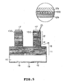
- Fig. 5 is a schematic sectional view of a vertical-cavity surface-emitting laser (VCSEL) as a second preferred embodiment of the present invention.
- the laser of the present embodiment has the same construction as that of the first embodiment except the p-type fourth semiconductor layer (i.e., AlGaAs/AlGaAs reflection layer) 12 which comprises two different types of AlGaAs layers 12a, 12b having different compositions.
- the p-type fourth semiconductor layer i.e., AlGaAs/AlGaAs reflection layer
- another type of AlGaAs layers 100 is further formed as a considerably thinner film provided between the above two different types of AlGaAs layers 12a, 12b.
- the AlGaAs layer 100 has a composition (hereinafter referred as a mid-composition) in which an amount of each constituent is almost in the middle of the range between that of the layers 12a, 12b.
- One of the two types of the AlGaAs layers which has a less Al content and a smaller band gap compared with that of the other type, is placed between the AlGaAs layers having larger band gaps. It is noted that the above AlaGAs layer 100 having the intermediate composition may be only formed between the smaller band group AlGaAs and the larger band gap AlGaAs placed on the active layer's side.
- the AlGaAs layer 100 having the mid-composition assists for holes to move onto the AlGaAs having a larger band gap after passing over the band-discontinuity of the valence band.
- the AlGaAs layer 100 is formed as an extremely thin film, as described above, so that it prevents the change in optical properties of the reflection layer to be caused by inserting a new layer. It means that a resistance of the p-type multiple layered structure to be provided as a reflection layer of the present invention, which tends to become higher even if the doping concentration is higher than usual, becomes lower than usual as a result of inserting the additional layer of AlGaAs formed as an extremely thin film made of the mid-composition. In this case, furthermore, the change in optical properties of the p-type multiple layered structure can be substantially disregarded.
- Figs. 6A to 6C are cross-sectional views of three epitaxial structures and Figs. 7A and 7B are cross-sectional views of wafer-fused structure for explaining the process for manufacturing the VCSEL of the present embodiment.
- n-AlAs layers and n-GaAs layers are epitaxially grown in alternating manner on the n-type GaAs substrate 60 to make 27 pairs thereof as a n-type AlAs/GaAs reflection layer 61, in which each of the layers has a thickness corresponding to a quarter of 1.55 ⁇ m optical length.
- a p-type InGaAsP/InP reflection layer 63 is formed on a p-type InP substrate 65 by an epitaxial growth of 10 pairs of P-InGaAsP layer and P-InP layer, in which each of the layers has a thickness corresponding to a quarter of 1.55 ⁇ m optical length.
- an InGaAsP (bulk) active layer 64 is epitaxially formed as one having a thickness corresponding to 1.55 ⁇ m optical length, followed by epitaxially forming an n-type InGaAsP/InP reflection layer 62 using n-InGaAsP layers and n-InP layers in alternating manner as 10.5 pairs thereof, in which each layer has a thickness corresponding to a quarter of 1.55 ⁇ m optical length.
- a surface of the epitaxially layered structure on the GaAs substrate 60 is treated with a solution of HF, while a surface of the epitaxially layered structure on the InP substrate 65 is treated with solutions of H 2 SO 4 :H 2 O 2 :H 2 O (3:1:1) and HF to remove naturally-oxidized films on their surfaces.
- the former surface is brought into intimate contact with the latter surface and loaded in a hydrogen atmosphere, followed by an annealing at 600°C for 1 hour to form a wafer-fused structure.
- the InP substrate 65 is etched down by a solution of HCl:H 3 PO 4 (3:1) so as to expose a surface of the InGaAsP layer of the p-type InGaAsP/InP reflection layer.
- the exposed p-InGaAsP layer is etched down by a solution of H 2 SO 4 :H 2 O 2 :H 2 O (3:1:1) to make a surface of the p-InP layer appear.
- an AlAs/AlGaAs/GaAs reflection layer 66 is formed on a p-type GaAs substrate 67 by epitaxially growing C-doped AlAs, GaAs, and Al 0.5 G 0.05 As layers in alternating manner on the GaAs substrate 67 to make a stack of 27 pairs thereof in which the AlAs and GaAs layers have the thickness of a quarter of 1.55 ⁇ m optical length, respectively, while the Al 0.5 G 0.05 As layer has a thickness of 10 nm.
- a surface of the epitaxially layered structure is subjected to the same treatment as described above, and then the top surface of thereof (i.e., p-GaAs layer) is brought into contact with the p-InP layer positioned at the top of the above wafer-fused structure. Then the resulting structure is subjected to an annealing in a hydrogen atmosphere at a temperature of 600 °C for 1 hour. After that, the p-type GaAs substrate 67 is removed by a solution of ammonia water and hydrogen peroxide water to expose a surface of the reflection layer 66.
- Circular patterns of 5 ⁇ m in diameter are formed on the exposed surface of the reflection layer 66 by photolithography, Furthermore, the reflection layer 66 is subjected to a reactive ion beam etching (RIBE) using a Cl 2 based gas at an accelerating voltage of 400 V to etch into the InGaAs/InP layer 62 under the active layer, and then a surface thereof is washed by a solution of HCl:H 2 PO 4 (3:1) as a selective etching solution for InGaAsP to expose a surface of the InP layer.
- RIBE reactive ion beam etching
- AuZnNi/Au electrodes 71 are deposited on the top of the device, while AuGeNi/Au electrodes 73 are deposited on the underside of the device.
- AR coat layers 72 are formed on the underside of the device to be used as an output portion.
- the AlAs/GaAs multi-layered films are used as the reflection layers but not limited to. It is possible to provide one of the reflection layers as a dielectric multi-layered film.
- the bulk of InGaAsP was used as the active layer but not limited to.
- the same effects can be attained by providing a strained layer MQW active layer or a non-strained MQW active layer made of InGaAsP/InGaAs.
- Fig. 8 is a schematic sectional view of a vertical-cavity surface-emitting laser (VCSEL) as a third preferred embodiment of the present invention.
- the laser of the present embodiment has the same construction as that of the second embodiment except in the follows.
- a n-type first semiconductor (AlGaAs/AlGaAs reflection layer) 11 comprises two different types of AlGaAs layers 11a, 11b having different compositions.
- another type of AlGaAs layers 100 is further formed as a considerably thinner film provided between the above two different types of AlGaAs layers 11a, 11b.
- a resistance of the n-type multiple layered structure is easy to be decreased as compared with that of the p-type one. In this case, however, it can be further decreased by inserting the above the additional layer of AlGaAs formed as an extremely thin film made of the mid-composition.
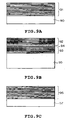
- Figs. 9A to 9C are cross-sectional views of three epitaxial structures and Figs. 10A and 10B are cross-sectional views of wafer-fused structure for explaining the process for manufacturing the VCSEL of the present embodiment.
- an AlAs/AlGaAs/GaAs reflection layer 91 is formed on a n-type GaAs substrate 90 by epitaxially growing n-type AlAs, GaAs, and Al 0.5 Ga 0.5 As layers in alternating manner on the GaAs substrate 90 to make a stack of 27 pairs thereof in which the AlAs and GaAs layers have the thickness corresponding to a quarter of 1.55 ⁇ m optical length, respectively, while the Al 0.5 Ga 0.5 As layer has a thickness of 10 nm.
- a p-type InGaAsP/InP reflection layer 93 is formed on a p-type InP substrate 95 by an epitaxial growth of 10 pairs of p-InGaAsP layer and p-InP layer, in which each of the layers has a thickness corresponding to a quarter of 1.55 ⁇ m optical length.
- an InGaAsP (bulk) active layer 94 is epitaxially formed as one having a thickness corresponding to 1.55 ⁇ m optical length, followed by epitaxially forming an n-type InGaAsP/InP reflection layer 92 using n-InGaAsP layers and n-InP layers in alternating manner as 10.5 pairs thereof, in which each of the layer has a thickness corresponding to a quarter of 1.55 ⁇ m optical length.
- a surface of the epitaxially layered structure on the GaAs substrate 90 is treated with a solution of HF, while a surface of the epitaxially layered structure on the InP substrate 95 is treated with solutions of H 2 SO 4 :H 2 O 2 :H 2 O (3:1:1) and HF to remove naturally-oxidized films on their surfaces.
- the former surface is brought into intimate contact with the latter surface and loaded in a hydrogen atmosphere, followed by an annealing at 600 °C for 1 hour to form a wafer-fused structure.
- the InP substrate 95 is etched down by a solution of HCl:H 3 PO 4 (3:1) so as to expose a surface of the InGaAsP layer of the p-type InGaAsP/InP reflection layer 93.
- the exposed p-InGaAsP layer is etched down by a solution of H 2 SO 4 :H 2 O 2 :H 2 O (3:1:1) to make a surface of the p-InP layer appear.
- an AlAs/AlGaAs/GaAs reflection layer 96 is formed on a p-type GaAs substrate 97 by epitaxially growing C-doped AlAs, GaAs, and AlGaAs layers in alternating manner on the GaAs substrate 97 to make a stack of 27 pairs thereof, in which each of the layers has a thickness corresponding to a quarter of 1.55 ⁇ m optical length.
- a surface of the epitaxially layered structure is subjected to the same treatment as described above, and then the top surface of thereof (i.e., p-GaAs layer) is brought into contact with the p-InP layer positioned at the top of the above wafer-fused structure.
- the resulting structure is subjected to an annealing in a hydrogen atmosphere at a temperature of 600 °C for 1 hour. After that, the p-type GaAs substrate 97 is removed by a mixture solution of ammonia water and hydrogen peroxide water to expose a surface of the reflection layer 96.
- Circular patterns of 5 ⁇ m in diameter are formed on the exposed surface of the reflection layer 96 by the step of photolithography. Furthermore, the reflection layer 96 is subjected to a reactive ion beam etching (RIBE) using a Cl 2 based gas at an accelerating voltage of 400 V to etch into the InGaAs/InP layer 92 under the active layer, and then a surface thereof is washed by a solution of HCl:H 2 PO 4 (3:1) as a selective etching solution for InGaAsP to expose a surface of the InP layer.
- RIBE reactive ion beam etching
- AuZnNi/Au electrodes 901 are deposited on the top of the device, while AuGeNi/Au electrodes 903 are deposited on the underside of the device.
- AR coat layers 902 are formed on the underside of the device to be used as an output portion.
- the AlAs/GaAs multi-layered films are used as the reflection layers but not limited to. It is possible to provide one of the reflection layers as a dielectric multi-layered film.
- the bulk of InGaAsP was used as the active layer but not limited to.
- the same effects can be attained by providing a strained layer MQW active layer or a non-strained MQW active layer made of InGaAsP/InGaAs.
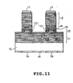
- Fig. 11 is a schematic sectional view of a vertical-cavity surface-emitting laser (VCSEL) as a fourth preferred embodiment of the present invention.
- the laser of the present embodiment has the same construction as that of the second embodiment except that an insulation layer 101 is formed by performing an ion-injection on the InGaAP/InGaAsP reflection layer 14. Therefore the active layer receives a high current injection as a current crowding effect, so that a less threshold current can be observed.
- the ion species is selected from light ions such as hydrogen, in general, ions are introduced deeply through the whole reflection layer and laterally distributed to damage the active layer. In this embodiment, however, there is no possibility of causing such a damage.
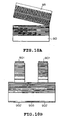
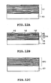
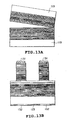
- Figs. 12A-12C and 13A-13B are cross-sectional views of the structures for explaining each step of the process for manufacturing a log-wavelength VCSEL of the present embodiment.
- a first reflection layer 111 is formed on a n-type GaAs substrate 113 by epitaxially growing n-GaAs and AlAs layers with a dopant of 3 x 10 18 cm -3 in alternating manner to make a stack of 25 pairs thereof on the GaAs substrate 113, in which each of layer has a thickness corresponding to a quarter of 1.55 ⁇ m optical length.
- a fourth reflection layer 120 is formed on a p-GaAs substrate 121 by epitaxially growing p-GaAs, AlGaAs, and AlAs layers in alternating manner to make a stack of 30 pairs thereof on the p-GaAs substrate 121, in which each of layer has a thickness of a quarter of 1.55 ⁇ m optical length.
- P-InGaAsP layer and P-InP layers are epitaxially grown in alternating manner on a p-type InP substrate 119 to make 5 pairs thereof as a p-type InGaAsP/InP reflection layer 116 with a thickness corresponding to a quarter of 1.55 ⁇ m optical length.
- an InGaAsP (bulk) active layer 114 is epitaxially formed as one having a thickness corresponding to 1.55 ⁇ m optical length, followed by epitaxially forming an n-type InGaAsP/InP reflection layer 118 using n-InGaAsP layers and n-InP layers in alternating manner as 5.5 pairs thereof, in which each of the layers has a thickness corresponding to a quarter of 1.55 ⁇ m optical length.
- Circular photoresist patterns of 10 ⁇ m in diameter are formed on the top of the epitaxially grown layers on the InP substrate 119, and then oxygen ions of 2 x 10 14 cm -3 are introduced therein at an acceleration voltage of 80 keV to make insulation regions 112. After removing the photoresist, the resulting structure is subjected to an annealing in a hydrogen atmosphere at temperature of 450 °C.
- Naturally-oxidized films on the first reflection layer 111 and the n-type InGaAsP/InP reflection layer 118 are removed by treating with a solution of HF, then the former surface is brought into intimate contact with the latter surface and loaded in a hydrogen atmosphere, followed by an annealing at 600 °C to form a wafer-fused structure as shown in Fig. 13A.
- the InP substrate 119 is removed by means of etching.
- a naturally-oxidized film of the fourth reflection layer 120 on the p-GaAs substrate 121 is removed by a solution of HF. Then a surface of the reflection layer 120 is brought into intimate contact with a surface of the p-InGaAsP/p-InP reflection layer 116 and loaded in a hydrogen atmosphere, followed by an annealing at 600 °C to form a wafer-fused structure.
- the resulting wafer-fused structure is subjected to a mixture solution of ammonia water and hydrogen peroxide water to remove the p-type GaAs substrate 121 and to expose a surface of the AlAs layer. Then the exposed AlAs layer is further etched by a HF solution.
- the resulting structure is subjected to a reactive ion beam etching (RIBE) for the purpose of electrically dividing elements.
- RIBE reactive ion beam etching
- a p-type AuZnNi/Au electrodes 131 are deposited on the top of the device, while AuGeNi/Au electrodes 133 are deposited on the underside of the device.
- AR coat layers 132 are formed on the underside of the device to be used as an output portion.
- the light-current characteristics of the long-wavelength VCSEL obtained by the above process revealed that the laser was oscillated at the threshold current of 4 mA with an oscillation wavelength of 1.55 ⁇ m, In this case, furthermore, there was no current crowded region in the p-type reflection layer with high resistance, so that the device resistance takes a small value as 20 ⁇ at a current in approximity to the threshold.
- the semiconductor multi-layered films are used as the reflection layers but not limited to. It is also possible to provide one of the reflection layers as a dielectric multi-layered film.
- the electrode on the side of the dielectric multi-layered film may be formed as in the same way as that of the conventional VCSEL that uses the dielectric multi-layered film.
- oxygen ions are introduced for preparing the current crowed region. In this case, however, it is possible to use other ions to get the same effects as that of the oxygen-injection.
- the bulk of InGaAsP was used as the active layer but not limited to.
- the same effects can be attained by providing a strained layer MQW active layer or a non-strained MQW active layer made of InGaAsP/InGaAs.
- Fig. 14 is a schematic sectional view of a vertical-cavity surface-emitting laser as a fifth preferred embodiment of the present invention.
- the laser of the present embodiment has the same construction as that of the second embodiment except that non-doping layers are formed between the active layer 15 and InGaAP/InGaAsP reflection layers 13, 14, respectively, followed by introducing impurities into each of them to form conductive layers 102.
- the active layer receives a current with a current crowding effect, so that a less threshold current can be observed.
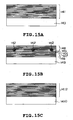
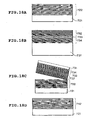
- Figs. 15A-15C and Figs. 16A-16C are cross-sectional views of the structures for explaining each step of the process for manufacturing a log-wavelength VCSEL of the present embodiment.
- a first reflection layer 141 is formed on a n-type GaAs substrate 143 by epitaxially growing n-GaAs and AlAs layers in alternating manner to make a stack of 25 pairs thereof on the GaAs substrate 143, in which each of layer has a thickness corresponding to a quarter of 1.55 ⁇ m optical length.
- a second reflection layer 1412 is formed on a p-GaAs substrate 1410 by epitaxially growing p-GaAs, AlGaAs, and AlAs layers in alternating manner to make a stack of 30 pairs thereof on the p-GaAs substrate 1410, in which each of layer has a thickness corresponding to a quarter of 1.55 ⁇ m optical length.
- p-InGaAsP layer and p-InP layers are epitaxially grown in alternating manner on a p-type InP substrate 149 to make 5 pairs thereof as a p-type InGaAsP/InP reflection layer 146, in which each of the layer has a thickness corresponding to a quarter of optical length. Then a non-doped InP cladding layer 147 is formed on the reflection layer 146.
- a multiple quantum well (MQW) active layer 144 is formed by piling up InGaAsP (1.3 ⁇ m composition) layers and InGaAs layers in alternating manner to make a 5.5 pairs thereof on the InP cladding layer 147. Then a non-doped InP cladding layer 145 is formed on the MQW active layer 144, and also n-InGaAs layers and n-InP layers are epitaxially grown in alternating manner on the non-doped cladding layer 145 to make 5.5 pairs thereof as an n-type InGaAs/InP reflection layer 148, in which each of the layer has a thickness corresponding to a quarter of optical length.
- InGaAsP 1.3 ⁇ m composition
- Circular photoresist patterns of 10 ⁇ m in diameter are formed on the top of the epitaxially grown layers on the InP substrate 149, and then Si ions are introduced therein at an acceleration voltage of 100 keV to make doped regions 142 with the dose of 2 x 10 16 cm -3 , After removing the photoresist, the resulting structure is subjected to an annealing in a hydrogen atmosphere at temperature of 450 °C.
- Naturally-oxidized films on the epitaxially grown layers on the n-GaAs and p-InP substrates 143, 149 are removed by treating with a solution of HF, then the former surface is brought into intimate contact with the latter surface and loaded in a hydrogen atmosphere, followed by an annealing at 600 °C to form a wafer-fused structure as shown in Fig. 16A.
- the InP substrate 149 is removed by means of etching.
- Circular photoresist patterns of 10 ⁇ m in diameter are formed on the resulting structure, and then Be ions are introduced therein at an acceleration voltage of 100 keV to make doped regions 151 with the dose of 2 ⁇ 10 16 cm -3 .
- the resulting structure is subjected to an annealing in a hydrogen atmosphere at temperature of 450 °C.
- Naturally-oxidized films on the epitaxially grown layers on the p-GaAs substrate 1410 are removed by treating with a solution of HF, then it is brought into intimate contact with the p-InGaAsP/p-InP reflection layer and loaded in a hydrogen atmosphere, followed by an annealing at 600 °C for 1 hour.
- a mixture solution of ammonia water and hydrogen peroxide the p-GaAs substrate 1410 is removed by means of etching.
- the AlAs layer, a part of the reflection layer is etched down by an aqueous solution of HF.
- p-type AuZnNi/Au electrodes 154 are deposited on the top of the device, while AuGeNi/Au electrodes 153 are deposited on the underside of the device.
- AR coat layers 152 are formed on the underside of the device to be used as an output portion.
- the distributed Bragg reflectors (DBR) layer is subjected to a reactive ion beam etching (RIBE) as shown in Fig. 16C.
- RIBE reactive ion beam etching
- the light-current characteristics of the long-wavelength VCSEL obtained by the above process revealed that the laser was oscillated at the threshold current of 6 mA.
- the semiconductor multi-layered films are used as the reflection layers but not limited to. It is possible to provide one of the reflection layers as a dielectric multi-layered film.
- the electrode on the side of the dielectric multi-layered film may be formed as in the same way as that of the conventional VCSEL that uses the dielectric one.
- a dopant is introduced into the cladding layer.
- the bulk of InGaAsP was used as the active layer but not limited to.
- the same effects can be attained by providing a strained layer MQW active layer or a non-strained MQW active layer made of InGaAsP/InGaAs.
- Fig. 17 is a schematic sectional view of a vertical-cavity surface-emitting laser (VCSEL) as a sixth preferred embodiment of the present invention.
- the laser of the present embodiment has a buried hetero-structure as shown in the figure.
- a VCSEL consists of a plurality of stacked layers on an n-type GaAs substrate 721.
- AuGeNi/Au electrodes 753 and anti-reflection films 754 are provided on one surface (i.e., a bottom surface) of the GaAs substrate 721, while on the other surface thereof (i.e., an upper surface) there are stacked an n-type AlAs/GaAs reflection layer 722, an n-type InGaAsP/InP reflection layer 732, an InGaAsP active layer 733, a p-type InGaAsP/InP reflection layer 734, and a p-type AlAs/Al 0.5 Ga 0.5 As/GaAs reflection layer 742 in that order.
- a mesa structure is formed by etching down from an upper surface of the top layer (i.e., the p-type AlAs/Al 0.5 Ga 0.5 As/GaAs reflection layer 742) to a certain point of the n-type InGaAsP/InP reflection layer 722. Furthermore, a buried layer of n-InP/p-InP/n-InP/p-InP 751 is formed on the mesa structure. In addition, an AuZnNi/Au electrodes 752 is provided on the upper surface of the p-type AlAs/Al 0.5 Ga 0.5 As/GaAs reflection layer 742.
- Figs. 18A to 18D are cross-sectional views of the structures for explaining each step of the process for manufacturing the VCSEL having the above buried hetero-structure.
- an AlAs/GaAs reflection layer 722 is formed on a n-type GaAs substrate 721. That is, AlAs layers and GaAs layers are epitaxially grown in alternating manner on the n-type GaAs substrate 721 to make 27 pairs thereof as the n-type AlAs/GaAs reflection layer 722, in which each of the layers has a thickness corresponding to a value obtained by dividing the emission wavelength (1.55 ⁇ m) by a refractive index and 4 (i.e., a thickness corresponding to a quarter of optical length for the emission wavelength).
- a p-type InGaAsP/InP reflection layer 734 is formed on a p-type InP substrate 731 by an epitaxial growth of 10.5 pairs of p-InGaAsP layer and p-InP layer in that order, in which each of the layers has a thickness corresponding to a quarter of 1.55 ⁇ m optical length.
- an InGaAsP (bulk) active layer 733 is epitaxially formed as one having a thickness corresponding to 1.55 ⁇ m optical length, followed by epitaxially forming an n-type InGaAsP/InP reflection layer 732 using n-InGaAsP layers and n-InP layers in alternating manner as 10 pairs thereof, in which each of the layers has a thickness corresponding to a quarter of 1.55 ⁇ m optical length.
- a surface of the epitaxial layer 722 on the GaAs substrate 721 is treated with HF, while a surface of the epitaxial layer 732 is treated with solutions of H 2 SO 4 :H 2 O 2 :H 2 O (3:1:1) and HF to remove naturally-oxidized films on their surfaces, and then, as shown in Fig. 18C, the former surface is brought into intimate contact with the latter surface and loaded in a hydrogen atmosphere, following by an annealing at 600 °C for 1 hour.
- the InP substrate 731 is etched by a solution of HCl:H 3 PO 4 (3:1) so as to expose a surface of the p-type InGaAsP layer of the p-type InGaAsP/InP reflection layer 734.
- the exposed p-type InGaAsP layer is etched by a solution of H 2 SO 4 :H 2 O 2 :H 2 O (3:1:1) to make a surface of the p-InP layer appear.
- a p-type AlAs/Al 0.5 Ga 0.5 As/GaAs reflection layer 742 is formed by the steps of: epitaxially growing p-type AlAs layers, p-Al 0.5 Ga 0.5 As layers, and P-GaAs layers one after the other by turns, in which each of the p-type AlAs and P-GaAs layers is formed as one having a thickness corresponding to a quarter of 1.55 ⁇ m optical length, while each of the p-Al 0.5 Ga 0.5 As layers is formed as a comparatively very thin film.
- a surface of the obtained reflection layer 742 is subjected to the same treatment as described above. Then the p-GaAs layer positioned at the top of the epitaxial layer 742 on the p-type GaAs substrate 741 is brought into contact with the p-InP layer positioned at the top of the epitaxial layer 734 and loaded in a hydrogen atmosphere, followed by an annealing at 600 °C for 1 hour.
- the p-type GaAs substrate 741 is removed from the epitaxial layer 742 by treating with a mixture solution of a ammonia water and hydrogen peroxide, and then circular patterns of 5 ⁇ m in diameter are formed by the step of photolithography. Furthermore, the n-InGaAsP/InP reflection layer is subjected to a reactive ion beam etching (RIBE) using a Cl 2 based gas at an accelerating voltage of 400 V to etch into the n-InGaAsP/InP reflection layer under the active layer 733, and then a surface thereof is washed by a solution of HCl:H 3 PO 4 (3:1) as a selective etching solution for n-InGaAsP, resulting in a mesa structure.
- RIBE reactive ion beam etching
- an n-InP/p-InP/n-InP/p-InP buried layer 751 is formed on the mesa structure by growing thin layers of a n-InP, a p-InP, a n-InP, and a p-InP layer in that order, using a technique of metal organic chemical vapor deposition (MOCVD).
- MOCVD metal organic chemical vapor deposition
- AuZnNi/Au electrodes 752 are formed on the top of the device, while AuGeNi/Au electrodes 753 are formed on the underside of the device by evaporation, and then a AR coat layers 754 are formed on the underside thereof to be used as an output portion.
- the light-current characteristics of the VCSEL obtained by the above process revealed that the laser was oscillated at the threshold current of 0.9 mA. In this case, furthermore, up to 10 mA, the device showed a single transverse mode.
- the bulk of InGaAsP was used as the active layer but not limited to.
- the same effects can be attained by providing a strained layer MQW active layer or a non-strained MQW active layer made of InGaAsP/InGaAs.
- the p-type AlAs/Al 0.5 Ga 0.5 As/GaAs reflection layer that basically comprises AlAs and GaAs which are piled repeatedly.
- the multi-layer construction may be prepared by stacking three different type of layers by turns.
- each of the reflection layers is provided as a multi-layered film.
- one of these reflection layers may be a dielectric multi-layered film (SiO 2 /TiO 2 , Si/AlO 3 , Si/SiO 2 , or the like).
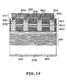
- Fig. 19 is a schematic cross sectional view of the seventh embodiment of the vertical-cavity surface-emitting laser (VCSEL) in accordance with the present invention.
- the device comprises a p-GaAs/AlAs reflector 851, a p-InP/InGaAsP reflector 852, a n-InP/InGaAsP reflector 853, an active layer 854, a n-InP buried layer 855, a Fe-doped InP buried layer 856, a reflector as a SiO 2 /TiO 2 dielectric multi-layered film 857, a p-type electrode 858, an anti-reflection (AR) coat film 859, and a n-type electrode 860.
- a p-GaAs/AlAs reflector 851 a p-InP/InGaAsP reflector 852, a n-InP/InGaAsP reflector 853, an active layer 854,
- the VCSEL is manufactured by the process including the steps of: epitaxially growing the layers of AlAs and GaAs by turns to form 25 pairs thereof on a p-type GaAs substrate, in which each layer has a thickness corresponding to a quarter of a predetermined optical length to form the p-GaAs/AlAs reflection layer 851; epitaxially growing the layers of n-InGaAsP and n-InP by turns to form 10.5 pairs thereof on a InP substrate to form the n-InP/InGaAsP reflector 853; forming an InGaAsP bulk active layer 854 with a thickness corresponding to an optical length, and epitaxially growing the layers of p-InGaAsP and p-InP by turns to form 10.5 pairs thereof to form the p-InP/InGaAsP reflection layer 852.
- the obtained structure is further subjected to the following steps of treating a surface of the epitaxial layer on the GaAs substrate with HF and treating a surface of the epitaxial layer on the InP substrate with HF and a solution of H 2 SO 4 :H 2 O 2 :H 2 O (3:1) to remove a naturally oxidized film; bringing these surfaces into intimate contact with each other; and subjecting in a hydrogen atmosphere to anneal at 600 °C for 1 hour, followed by removing the InP substrate using a solution of HCl:H 2 PO 4 (3:1).
- the n-InGaAsP/InP reflection layer 852 is subjected to a reactive ion beam etching (RIBE) using a gas of the mixture of ethane (C 2 H 2 ) and hydrogen to etch into the InP layer under the active layer, and then the InP layer is etched by HCl. Subsequently, the InGaAsP layer is etched down to a surface of the InP layer. After that, the Fe-doped InP layer 856 and the n-type InP layer are grown in order.
- RIBE reactive ion beam etching
- n-type electrodes 860 are formed on the top of the InP layers, respectively, and also the SiO 2 /TiO 2 dielectric multi-layered film is subsequently prepared by evaporation. Meanwhile, p-type electrodes 858 are formed on the underside of the GaAs substrate by evaporation, and then a AR coat layers 859 are formed on the underside thereof to be used as an output portion.
- the light-current characteristics of the VCSEL obtained by the above process revealed that the laser was oscillated at the threshold current of 0.9 mA. In this case, furthermore, up to 10 mA, the device showed a single transverse mode.
- each of the reflection layers is provided as a multi-layered film.
- one of these reflection layers may be a dielectric multi-layered film.
- the bulk of InGaAsP was used as the active layer but not limited to.
- the same effects can be attained by providing a strained layer MQW active layer or a non-strained MQW active layer made of InGaAsP/InGaAs.
- Fig. 20 is a schematic cross sectional view of the eighth embodiment of the vertical-cavity surface-emitting laser (VCSEL) in accordance with the present invention.
- the device comprises a p-GaAs/AlAs reflector 971, a p-InP/InGaAsP reflector 972, a InGaAsP bulk active layer 980, a n-InP/InGaAsP reflector 973, an InAlAs layer 974, a GaAs/AlAs layer 975, an InAlAs oxidized layer 976, a n-type contact 977, a p-type contact 978, and an anti-reflection (AR) coat film 979.
- AR anti-reflection
- the VCSEL is manufactured by the process including the following steps. At first, the layers of AlAs and GaAs are epitaxially grown by turns to form 25 pairs thereof on a p-type GaAs substrate, in which each layer has a thickness corresponding to a quarter of 1.55 ⁇ m optical length, to form the p-GaAs/AlAs reflection layer 971. On the other hand, the layers of n-InGaAsP and n-InP are epitaxially grown by turns to form 9 pairs thereof on a InP. substrate, in which each layer has a thickness of a quarter of 1.55 ⁇ m optical length, to form the n-InP/InGaAsP reflector 953.
- an InGaAsP bulk active layer 980 with a thickness corresponding to a 1.55 ⁇ m optical length is formed, and also the layers of p-InAlAs and p-InGaAsP are grown to form one pair thereof as the InAlAs layer 974. Furthermore, the layers of p-InP and p-InGaAsP are epitaxially grown by turns to form 9.5 pairs thereof to form the p-InP/InGaAsP reflector 972.
- the obtained structure is further subjected to the following steps of treating a surface of the epitaxial layer on the GaAs substrate with HF and treating a surface of the epitaxial layer on the InP substrate with solutions of HF and H 2 SO 4 :H 2 O 2 :H 2 O (3:1) to remove a naturally oxidized film, bringing these surfaces into intimate contact with each other and subjecting in a hydrogen atmosphere to anneal at 600 °C for 1 hour, followed by removing the InP substrate using a solution of HCl:H 2 PO 4 (3:1).
- n-GaAs/AlAs layer 975 is formed by epitaxially growing AlAs and GaAs layers on a GaAs substrate in alternating manner to make a stack of 20 pairs of the layers in which each of them has a thickness corresponding to a quarter of 1.55 ⁇ m optical length.
- the obtained structure is further subjected to the following steps of treating a surface of the epitaxial layer on the GaAs substrate with HF and treating a surface of the epitaxial layer on the InP substrate with solutions of HF and H 2 SO 4 :H 2 O 2 :H 2 O (3:1) to remove a naturally oxidized film, bringing these surfaces into intimate contact with each other and subjecting in a hydrogen atmosphere to anneal at 600 °C for 1 hour, followed by removing the GaAs substrate using a solution of HCl:H 2 PO 4 (3:1).
- SiO 2 circular patterns of 5 ⁇ m in diameter are formed by the step of photolithography.
- a reactive ion beam etching (RIBE) is performed using a gas of the mixture of argon and chloride to etch into the InGaAsP/InP layer under the active layer.
- a current crowding region (InAlAs oxidized layer) 976 is formed by laterally oxidizing the InAlAs in a water vapor at a temperature of 525 °C.
- the n-type electrodes 977 are formed, while p-type electrodes 978 are formed on the underside of the GaAs substrate.
- a AR coat layers 979 are formed on the underside thereof to be used as an output portion.
- the light-current characteristics of the VCSEL obtained by the above process revealed that the laser was oscillated at the threshold current of 0.6 mA.
- the cladding layer may be made of InGaAsP or InP with an appropriate thickness.
- wafer-fusion interfaces can be formed between the reflection layers of the first and second semiconductor multi-layered films and between the reflection layers of the third and fourth semiconductor multi-layered films, respectively, which are arranged on the upper or under side of the active layer. This fact allows a longer distance between the active layer and each of the fusion-interfaces without increasing a resonant cavity length, resulting in good crystallinity of the active layer. Then, a threshold current becomes low.
- the active layer can be grown on the same substrate together with the second and third reflection layers, so that it allows a measurement of oscillation wavelength before fusing the emission region with the substrate having the first or fourth reflection layer thereon.
- the InGaAsP based semiconductor multi-layered structure under the active layer so that it becomes possible to increase an acceptable depth of etching at the time of forming the buried hetero-structure and also it can be performed in conjunction with a selectable chemical etching.
- the etching depth can be easily regulated uniformly and it becomes possible to increase the yields at the time of forming the buried hetero-structure, dramatically. Therefore, the VCSEL can emit at a single transverse mode light under the condition of high-carrier injection density.
- the bulk of InGaAsP was used as the active layer but not limited to.
- the same effects can be attained by providing a strained layer MQW active layer or a non-strained MQW active layer made of InGaAsP/InGaAs.
Landscapes
- Physics & Mathematics (AREA)
- Optics & Photonics (AREA)
- Condensed Matter Physics & Semiconductors (AREA)
- General Physics & Mathematics (AREA)
- Electromagnetism (AREA)
- Chemical & Material Sciences (AREA)
- Engineering & Computer Science (AREA)
- Nanotechnology (AREA)
- Life Sciences & Earth Sciences (AREA)
- Biophysics (AREA)
- Crystallography & Structural Chemistry (AREA)
- Semiconductor Lasers (AREA)
Claims (18)
- Laser à semi-conducteur à émission de surface et à cavité verticale comprenant :une première feuille (11) semi-conductrice à couches multiples formée d'une pluralité de couches en Alx1Ga1-x1As (0 ≤ x1 ≤ 1) et d'une pluralité de couches en Alx2Ga1-x2As (0 ≤ x2 ≤ 1) disposées en alternance, dans laquelle chaque couche individuelle a une épaisseur égale à une valeur obtenue en divisant la longueur d'onde optique d'émission du laser par l'indice de réfraction correspondant de la couche individuelle et par 4 ;une interface à fusion de pastille entre la première feuille à couches multiples et une seconde feuille (13) semi-conductrice à couches multiples ;la seconde feuille semi-conductrice à couches multiples qui est formée d'une pluralité de couches en Inx3Ga1-x3Asy3P1-y3 (0 ≤ x3, y3 ≤ 1) et d'une pluralité de couches en Inx4Ga1-x4Asy4P1-y4 (0 ≤ x4, y4 ≤ 1) disposées en alternance, dans laquelle chaque couche individuelle a une épaisseur égale à une valeur obtenue en divisant la longueur d'onde optique d'émission du laser par l'indice de réfraction correspondant de la couche individuelle et par 4 ;une couche (15) active ayant une couche en Inx5Ga1-x5Asy5P1-y5 (0 ≤ x5, y5 ≤ 1) ;une troisième feuille (14) semi-conductrice à couches multiples formée d'une pluralité de couches en Inx6Ga1-x6Asy6P1-y6 (0 ≤ x6, y6 ≤ 1) et d'une pluralité de couches en Inx7Ga1-x7Asy7P1-y7 (0 ≤ x7, y7 ≤ 1) disposées en alternance, dans laquelle chaque couche individuelle a une épaisseur égale à une valeur obtenue en divisant la longueur d'onde optique d'émission du laser par l'indice de réfraction correspondant de la couche individuelle et par 4 ;la deuxième feuille semi-conductrice à couches multiples, la couche active et la troisième feuille semi-conductrice à couches multiples étant formées par épitaxie les unes sur les autres ;une interface à fusion de pastille entre la troisième feuille à couches multiples et une quatrième feuille (12) semi-conductrice à couches multiples ; etla quatrième feuille semi-conductrice à couches multiples qui est formée d'une pluralité de couches en Alx8Ga1-x8As (0 ≤ x8 ≤ 1) et d'une pluralité de couches en Alx9Ga1-x9As (0 ≤ x9 ≤ 1) disposées en alternance, dans laquelle chaque couche individuelle a une épaisseur égale à une valeur obtenue en divisant la longueur d'onde optique d'émission du laser par l'indice de réfraction correspondant de la couche individuelle et par 4, dans lequella première feuille (11) semi-conductrice à couches multiples, la deuxième feuille (12) semi-conductrice à couches multiples, la couche (15) active, la troisième feuille (14) semi-conductrice à couches multiples et la quatrième feuille (12) semi-conductrice à couches multiples sont disposées dans cet ordre sur un substrat (16) en GaAs.
- Laser à semi-conducteur à émission de surface et à cavité verticale suivant la revendication 1, dans lequel
la première feuille (11) semi-conductrice à couches multiples comprend en outre une pluralité de couches (100) en Alx10Ga1-x10As (0 ≤ x10 ≤ 1) de manière que chaque couche (100) en Alx10Ga1-x10As soit plus mince que la couche en Alx1Ga1-x1As et que la couche en Alx2Ga1-x2As et soit prévue entre la couche (11a) en Alx1Ga1-x1As et la couche (11b) en Alx2Ga1-x2As. - Laser à semi-conducteur à émission de surface et à cavité verticale suivant la revendication 1, dans lequel
la quatrième feuille (12) semi-conductrice à couches multiples comprend en outre une pluralité de couches (100) en Alx11Ga1-x11As (0 ≤ x11 ≤ 1) de manière que chaque couche en Alx11Ga1-x11As soit plus mince que la couche (12a) en Alx8Ga1-x8As et que la couche (12b) en Alx9Ga1-x9As et se trouve entre la couche en Alx8Ga1-x8As et la couche en Alx9Ga1-x9As. - Laser à semi-conducteur à émission de surface et à cavité verticale suivant la revendication 1, dans lequel la deuxième feuille (13) semi-conductrice à couches multiples comprend au moins une partie (101) de grande résistance servant de couche isolante formée par injection d'ion.
- Laser à semi-conducteur à émission de surface et à cavité verticale suivant la revendication 1, dans lequel chacune de la deuxième feuille (13) semi-conductrice à couches multiples et de la troisième feuille (14) semi-conductrice à couches multiples comprend une partie (102) conductrice servant de couche conductrice formée par une injection d'ion.
- Laser à semi-conducteur à émission de surface et à cavité verticale suivant la revendication 1, comprenant en outre :une structure mésa formée par attaque chimique vers le bas à partir de la quatrième feuille (12) semi-conductrice à couches multiples jusqu'à un point déterminé à l'avance de la deuxième feuille (13) semi-conductrice à couches multiples etune hétéro-structure (751) enterrée formée sur la structure mésa, dans laquellel'hétéro-structure enterrée est préparée en faisant croítre un semi-conducteur choisi dans un groupe de InP et d'autres semi-conducteurs qui ont des constantes de réseau s'adaptant à celui de InP.
- Laser à semi-conducteur à émission de surface et à cavité verticale suivant la revendication 1, comprenant en outre au moins une couche choisie parmi soit :dans lequelune couche en Inx12Al1-x13Ga1-x12-x13As (0 ≤ x12, x13 ≤ 1) formée entre la deuxième feuille (13) semi-conductrice à couches multiples et la couche (15) active ; soit,une couche en Inx12Alx13Ga1-x12-x13As (0 ≤ x12, x13 ≤ 1) formée entre la troisième feuille (14) semi-conductrice à couches multiples et la couche (15) active,
la couche sélectionnée comprend une partie oxydée. - Laser à semi-conducteur à émission de surface et à cavité verticale suivant la revendication 1, comprenant en outre au moins une couche choisie parmi soit :une couche de placage consistant en Inx14Ga1-x14As1-y14P1-y14 (0 ≤ x14, y14 ≤ 1) formée entre la couche (15) active et la deuxième feuille (11) semi-conductrice à couches multiples ; soitune couche de placage consistant en Inx14Ga1-x14As1-y14P1-y14 (0 ≤ x14, y14 ≤ 1) formée entre la couche active et la troisième feuille semi-conductrice à couches multiples.
- Laser à semi-conducteur à émission de surface et à cavité verticale suivant la revendication 1, comprenantune première feuille (11) semi-conductrice à couches multiples formée d'une pluralité de couches en Alx1Ga1-x1As (0 ≤ x1 ≤ 1) et d'une pluralité de couches en Alx2Ga1-x2As (0 ≤ x2 ≤ 1) disposées en alternance, dans laquelle chaque couche individuelle a une épaisseur égale à une valeur obtenue en divisant la longueur d'onde optique d'émission du laser par l'indice de réfraction correspondant de la couche individuelle et par 4 ;une interface à fusion de pastille entre la première feuille à couches multiples et une seconde feuille (13) semi-conductrice à couches multiples ;la seconde feuille semi-conductrice à couches multiples qui est formée d'une pluralité de couches en Inx3Ga1-x3Asy3P1-y3 (0 ≤ x3, y3 ≤ 1) et d'une pluralité de couches en Inx4Ga1-x4Asy4P1-y4 (0 ≤ x4, y4 ≤ 1) disposées en alternance, dans laquelle chaque couche individuelle a une épaisseur égale à une valeur obtenue en divisant la longueur d'onde optique d'émission du laser par l'indice de réfraction correspondant de la couche individuelle et par 4 ;une couche (15) active ayant une couche en Inx5Ga1-x5Asy5P1-y5 (0 ≤ x5, y5 ≤ 1);une troisième feuille (14) semi-conductrice à couches multiples formée d'une pluralité de couches en Inx6Ga1-x6Asy6P1-y6 (0 ≤ x6, y6 ≤ 1) et d'une pluralité de couches en Inx7Ga1-x7Asy7P1-y7 (0 ≤ x7, y7 ≤ 1) disposées en alternance, dans laquelle chaque couche individuelle a une épaisseur égale à une valeur obtenue en divisant la longueur d'onde optique d'émission du laser par l'indice de réfraction correspondant de la couche individuelle et par 4 ;la deuxième feuille semi-conductrice à couches multiples, la couche active et la troisième feuille semi-conductrice à couches multiples étant formées par épitaxie les unes sur les autres ; etune feuille diélectrique à couches multiples, dans laquellela première feuille (11) semi-conductrice à couches multiples, la deuxième feuille (12) semi-conductrice à couches multiples, la couche (15) active, la troisième feuille (14) semi-conductrice à couches multiples et la feuille (12) diélectrique à couches multiples sont disposées dans cet ordre sur un substrat (16) en GaAs.
- Laser à semi-conducteur à émission de surface et à cavité verticale suivant l'une des revendications 1 ou 9, dans lequel
la couche (15) active est une structure (144) à puits quantiques multiples. - Procédé de fabrication d'un laser à semi-conducteur à émission de surface et à cavité verticale qui consiste :à faire croítre une première feuille (31) semi-conductrice à couches multiples sur un premier substrat (30) en GaAs ;à faire croítre par épitaxie les uns sur les autres une troisième feuille (33) semi-conductrice à couches multiples, une couche (34) active, une deuxième feuille (32) semi-conductrice à couches multiples dans cet ordre, sur un substrat (35) en InP ;à faire croítre une quatrième feuille (36) semi-conductrice à couches multiples sur un deuxième substrat (37) en GaAs ;à fusionner la première feuille (31) semi-conductrice à couches multiples à la deuxième feuille (32) semi-conductrice à couches multiples sous l'action de la chaleur et de la pression puis à faire suivre de l'enlèvement du substrat (35) en InP ; età fusionner la troisième feuille (33) semi-conductrice à couches multiples et la quatrième feuille (36) semi-conductrice à couches multiples sous l'effet de la chaleur et de la pression puis à faire suivre de l'enlèvement du deuxième substrat (37) en GaAs, dans lequella première feuille semi-conductrice à couches multiples est formée en faisant croítre par épitaxie une pluralité de couches en Alx-1Ga1-x1As (0 ≤ x1 ≤ 1) et une pluralité de couches en Alx2Ga1-x2As (0 ≤ x2 ≤ 1) alternativement couche par couche, chaque couche individuelle ayant une épaisseur égale à une valeur obtenue en divisant la longueur d'onde optique d'émission du laser par l'indice de réfraction correspondant de la couche individuelle et par 4 ;la troisième feuille semi-conductrice à couches multiples est formée en faisant croítre par épitaxie une pluralité de couches en Inx3Ga1-x3Asy3P1-y3 (0 ≤ x3, y3 ≤ 1) et une pluralité de couches en Inx4Ga1-x4Asy4P1-y4 (0 ≤ x4, y4 ≤ 1) en alternance couche par couche, chaque couche individuelle ayant une épaisseur égale à une valeur obtenue en divisant la longueur d'onde optique d'émission du laser par l'indice de réfraction correspondant de la couche individuelle et par 4 ;la couche active est formée d'au moins une couche en Inx5Ga1-x5Asy5P1-y5 (0 ≤ x5, y5 ≤ 1);la deuxième feuille semi-conductrice à couches multiples est formée en faisant croítre par épitaxie une pluralité de couches en Inx6Ga1-x6Asy6P1-y6 (0 ≤ x6, y6 ≤ 1) et une pluralité de couches en InxyGa1-x7Asy7P1-y7 (0 ≤ xy, y7 ≤ 1) en alternance couche par couche, chaque couche individuelle ayant une épaisseur égale à une valeur obtenue en divisant la longueur d'onde optique d'émission du laser par l'indice de réfraction correspondant de la couche individuelle et par 4 ; etla quatrième feuille semi-conductrice à couches multiples est formée en faisant croítre par épitaxie une pluralité de couches en Alx8Ga1-x8As (0 ≤ x8 ≤ 1) et une pluralité de couches en Alx9Ga1-x9As (0 ≤ x9 ≤ 1) en alternance couche par couche, chaque couche individuelle ayant une épaisseur égale à une valeur obtenue en divisant la longueur d'onde optique d'émission du laser par l'indice de réfraction correspondant de la couche individuelle et par 4.
- Procédé suivant la revendication 11, dans lequel
le stade de croissance de la première feuille (31) semi-conductrice à couches multiples sur le substrat (30) en GaAs comprend en outre un stade de croissance d'une couche (100) en Alx10Ga1-x10As (0 ≤ x10 ≤ 1) entre la couche en Alx1Ga1-x1As et la couche en Alx2Ga1-x2As, la couche en Alx10Ga1-x10As étant plus mince que la couche en Alx1Ga1-x1As et que la couche en Alx2Ga1-x2As. - Procédé suivant la revendication 11, dans lequel
le stade de croissance de la quatrième feuille (36) semi-conductrice à couches multiples sur le deuxième substrat (37) en GaAs comprend en outre un stade de croissance d'une couche (100) en Alx11G1-x11As (0 ≤ x11 ≤ 1) entre la couche en Alx8Ga1-x8As et la couche en Alx8Ga1-x8As, la couche en Alx11Ga1-x11As étant plus mince que la couche en Alx8Ga1-x8As et que la couche en Alx8Ga1-x8As. - Procédé suivant la revendication 11, dans lequel
avant d'enlever le substrat (35) en InP, on forme au moins une partie (101) de grande résistance en tant que couche isolante dans au moins l'une des deuxièmes feuilles (32) semi-conductrices à couches multiples et troisièmes feuilles (33) semi-conductrices à couches multiples par injection d'ion. - Procédé suivant la revendication 11, dans lequel
avant de fusionner la troisième feuille (33) semi-conductrice à couches multiples et la quatrième feuille (36) semi-conductrice à couches multiples, on forme au moins une partie (102) conductrice en tant que couche conductrice dans chacune des deuxièmes feuilles (32) semi-conductrices à couches multiples et troisièmes feuilles (33) semi-conductrices à couches multiples par injection d'ion. - Procédé suivant la revendication 11, dans lequelaprès avoir enlevé le deuxième substrat (37) en GaAs, on forme une structure mesa en attaquant chimiquement vers le bas à partir de la quatrième feuille (36) semi-conductrice à couches multiples jusqu'à un point déterminé à l'avance de la deuxième feuille (32) semi-conductrice à couches multiples ; eton forme une hétéro-structure (751) enterrée sur la structure mesa en faisant croítre un semi-conducteur choisi dans le groupe de InP et d'autres semi-conducteurs qui ont des constantes de réseau s'adaptant à celles de InP.
- Procédé suivant la revendication 11, dans lequelavant d'enlever le substrat (35) en InP, on forme une première couche en Inx12Alx13Ga1x12x13As (0 ≤ x12, x13 ≤ 1) entre la deuxième feuille (32) semi-conductrice à couches multiples et la couche (34) active et on forme une deuxième couche en Inx12Alx13Ga1-x12-x13As (0 ≤ x12, x13 ≤ 1) entre la troisième feuille (33) semi-conductrice à couches multiples et la couche (34) active etaprès avoir formé une structure mesa, on forme une partie oxydée dans la première et la deuxième couche en Inx12Alx13Ga1-x12-x13As.
- Procédé suivant la revendication 11, comprenant au moins un stade de formation d'une couche de placage consistant en Inx14Ga1-x14As1-x14P1-y14 (0 ≤ x14, y14 < 1) sur au moins l'une de l'interface comprise entre la couche (34) active et la deuxième feuille (32) semi-conductrice à couches multiples et de l'interface comprise entre la couche (34) active et la troisième feuille (33) semi-conductrice à couches multiples.
Applications Claiming Priority (3)
| Application Number | Priority Date | Filing Date | Title |
|---|---|---|---|
| JP338565/95 | 1995-12-26 | ||
| JP33856595 | 1995-12-26 | ||
| JP33856595 | 1995-12-26 |
Publications (3)
| Publication Number | Publication Date |
|---|---|
| EP0784363A2 EP0784363A2 (fr) | 1997-07-16 |
| EP0784363A3 EP0784363A3 (fr) | 1998-05-06 |
| EP0784363B1 true EP0784363B1 (fr) | 2000-10-11 |
Family
ID=18319378
Family Applications (1)
| Application Number | Title | Priority Date | Filing Date |
|---|---|---|---|
| EP96309451A Expired - Lifetime EP0784363B1 (fr) | 1995-12-26 | 1996-12-23 | Laser à émission de surface à cavité verticale et son procédé de fabrication |
Country Status (3)
| Country | Link |
|---|---|
| US (2) | US5864575A (fr) |
| EP (1) | EP0784363B1 (fr) |
| DE (1) | DE69610610T2 (fr) |
Families Citing this family (35)
| Publication number | Priority date | Publication date | Assignee | Title |
|---|---|---|---|---|
| US6148016A (en) * | 1997-11-06 | 2000-11-14 | The Regents Of The University Of California | Integrated semiconductor lasers and photodetectors |
| GB2333895B (en) * | 1998-01-31 | 2003-02-26 | Mitel Semiconductor Ab | Pre-fusion oxidized and wafer-bonded vertical cavity laser |
| US6549553B1 (en) | 1998-02-25 | 2003-04-15 | Nippon Telegraph And Telephone Corporation | Vertical-cavity surface-emitting semiconductor laser |
| US6117699A (en) * | 1998-04-10 | 2000-09-12 | Hewlett-Packard Company | Monolithic multiple wavelength VCSEL array |
| US7167495B2 (en) * | 1998-12-21 | 2007-01-23 | Finisar Corporation | Use of GaAs extended barrier layers between active regions containing nitrogen and AlGaAs confining layers |
| US7408964B2 (en) | 2001-12-20 | 2008-08-05 | Finisar Corporation | Vertical cavity surface emitting laser including indium and nitrogen in the active region |
| US6975660B2 (en) | 2001-12-27 | 2005-12-13 | Finisar Corporation | Vertical cavity surface emitting laser including indium and antimony in the active region |
| US7257143B2 (en) * | 1998-12-21 | 2007-08-14 | Finisar Corporation | Multicomponent barrier layers in quantum well active regions to enhance confinement and speed |
| US7286585B2 (en) | 1998-12-21 | 2007-10-23 | Finisar Corporation | Low temperature grown layers with migration enhanced epitaxy adjacent to an InGaAsN(Sb) based active region |
| US7058112B2 (en) | 2001-12-27 | 2006-06-06 | Finisar Corporation | Indium free vertical cavity surface emitting laser |
| US6922426B2 (en) | 2001-12-20 | 2005-07-26 | Finisar Corporation | Vertical cavity surface emitting laser including indium in the active region |
| US20030219917A1 (en) * | 1998-12-21 | 2003-11-27 | Johnson Ralph H. | System and method using migration enhanced epitaxy for flattening active layers and the mechanical stabilization of quantum wells associated with vertical cavity surface emitting lasers |
| US7435660B2 (en) * | 1998-12-21 | 2008-10-14 | Finisar Corporation | Migration enhanced epitaxy fabrication of active regions having quantum wells |
| US7095770B2 (en) | 2001-12-20 | 2006-08-22 | Finisar Corporation | Vertical cavity surface emitting laser including indium, antimony and nitrogen in the active region |
| US6320206B1 (en) | 1999-02-05 | 2001-11-20 | Lumileds Lighting, U.S., Llc | Light emitting devices having wafer bonded aluminum gallium indium nitride structures and mirror stacks |
| US6280523B1 (en) * | 1999-02-05 | 2001-08-28 | Lumileds Lighting, U.S., Llc | Thickness tailoring of wafer bonded AlxGayInzN structures by laser melting |
| US6975663B2 (en) * | 2001-02-26 | 2005-12-13 | Ricoh Company, Ltd. | Surface-emission laser diode operable in the wavelength band of 1.1-7μm and optical telecommunication system using such a laser diode |
| WO2001031756A1 (fr) * | 1999-10-29 | 2001-05-03 | E20 Communications, Inc. | Lasers integres modules a cavite verticale, a emission par la surface et a pompage optique |
| US6424669B1 (en) * | 1999-10-29 | 2002-07-23 | E20 Communications, Inc. | Integrated optically pumped vertical cavity surface emitting laser |
| US6631154B2 (en) | 2000-08-22 | 2003-10-07 | The Regents Of The University Of California | Method of fabricating a distributed Bragg reflector having enhanced thermal and electrical properties |
| US20020075926A1 (en) | 2000-08-22 | 2002-06-20 | Coldren Larry A. | Current leveling layer integrated with aperture for intracavity device |
| AUPR137700A0 (en) * | 2000-11-09 | 2000-11-30 | Australian National University, The | A steerable vertical cavity surface emitting laser |
| US6556610B1 (en) | 2001-04-12 | 2003-04-29 | E20 Communications, Inc. | Semiconductor lasers |
| US6717964B2 (en) | 2001-07-02 | 2004-04-06 | E20 Communications, Inc. | Method and apparatus for wavelength tuning of optically pumped vertical cavity surface emitting lasers |
| KR100446615B1 (ko) * | 2001-10-09 | 2004-09-04 | 삼성전자주식회사 | 반도체 레이저 다이오드 및 그 제조방법 |
| JP4066654B2 (ja) * | 2001-12-19 | 2008-03-26 | 富士ゼロックス株式会社 | 面発光型半導体レーザ装置及びその製造方法 |
| US6822995B2 (en) * | 2002-02-21 | 2004-11-23 | Finisar Corporation | GaAs/AI(Ga)As distributed bragg reflector on InP |
| US7295586B2 (en) | 2002-02-21 | 2007-11-13 | Finisar Corporation | Carbon doped GaAsSb suitable for use in tunnel junctions of long-wavelength VCSELs |
| US6798806B1 (en) * | 2002-09-03 | 2004-09-28 | Finisar Corporation | Hybrid mirror VCSELs |
| US7433381B2 (en) * | 2003-06-25 | 2008-10-07 | Finisar Corporation | InP based long wavelength VCSEL |
| US7860137B2 (en) | 2004-10-01 | 2010-12-28 | Finisar Corporation | Vertical cavity surface emitting laser with undoped top mirror |
| CN101432936B (zh) | 2004-10-01 | 2011-02-02 | 菲尼萨公司 | 具有多顶侧接触的垂直腔面发射激光器 |
| KR100990702B1 (ko) * | 2006-08-23 | 2010-10-29 | 가부시키가이샤 리코 | 면 발광 레이저 어레이, 광학 주사 장치 및 화상 형성 장치 |
| JP2008053353A (ja) * | 2006-08-23 | 2008-03-06 | Ricoh Co Ltd | 面発光レーザアレイ、それに用いられる面発光レーザ素子および面発光レーザアレイの製造方法 |
| TWI694649B (zh) * | 2019-08-05 | 2020-05-21 | 聯勝光電股份有限公司 | 高散熱的面射型雷射結構 |
Family Cites Families (9)
| Publication number | Priority date | Publication date | Assignee | Title |
|---|---|---|---|---|
| US5206871A (en) * | 1991-12-27 | 1993-04-27 | At&T Bell Laboratories | Optical devices with electron-beam evaporated multilayer mirror |
| JP3244529B2 (ja) * | 1992-04-16 | 2002-01-07 | アジレント・テクノロジーズ・インク | 面発光型第2高調波生成素子 |
| US5343487A (en) * | 1992-10-01 | 1994-08-30 | Optical Concepts, Inc. | Electrical pumping scheme for vertical-cavity surface-emitting lasers |
| JP3097938B2 (ja) * | 1992-10-06 | 2000-10-10 | 日本電信電話株式会社 | 面発光半導体レーザ |
| SE501635C2 (sv) * | 1993-08-20 | 1995-04-03 | Asea Brown Boveri | Förfarande och anordning för utsändande av ljus med integrerad excitationskälla |
| JPH07335967A (ja) | 1994-06-07 | 1995-12-22 | Oki Electric Ind Co Ltd | 面発光型光半導体素子及びその製造方法 |
| US5432809A (en) * | 1994-06-15 | 1995-07-11 | Motorola, Inc. | VCSEL with Al-free cavity region |
| JPH0878776A (ja) * | 1994-09-06 | 1996-03-22 | Fuji Xerox Co Ltd | 半導体レーザ装置 |
| US5493577A (en) * | 1994-12-21 | 1996-02-20 | Sandia Corporation | Efficient semiconductor light-emitting device and method |
-
1996
- 1996-12-23 EP EP96309451A patent/EP0784363B1/fr not_active Expired - Lifetime
- 1996-12-23 DE DE69610610T patent/DE69610610T2/de not_active Expired - Lifetime
- 1996-12-24 US US08/777,975 patent/US5864575A/en not_active Expired - Lifetime
-
1998
- 1998-09-28 US US09/162,235 patent/US6127200A/en not_active Expired - Fee Related
Also Published As
| Publication number | Publication date |
|---|---|
| US6127200A (en) | 2000-10-03 |
| EP0784363A2 (fr) | 1997-07-16 |
| EP0784363A3 (fr) | 1998-05-06 |
| DE69610610D1 (de) | 2000-11-16 |
| DE69610610T2 (de) | 2001-05-03 |
| US5864575A (en) | 1999-01-26 |
Similar Documents
| Publication | Publication Date | Title |
|---|---|---|
| EP0784363B1 (fr) | Laser à émission de surface à cavité verticale et son procédé de fabrication | |
| US6320893B1 (en) | Surface emitting semiconductor laser | |
| US6898226B2 (en) | Surface emitting semiconductor laser and process for producing the same | |
| US8189642B1 (en) | VCSEL semiconductor device | |
| JP4265875B2 (ja) | 面発光半導体レーザの製造方法 | |
| JP4602701B2 (ja) | 面発光レーザ及び光伝送システム | |
| JP4594814B2 (ja) | フォトニック結晶レーザ、フォトニック結晶レーザの製造方法、面発光レーザアレイ、光伝送システム、及び書き込みシステム | |
| JPH0669585A (ja) | 面発光半導体レーザ及びその製造方法 | |
| JP2003133640A (ja) | 面発光半導体レーザ素子 | |
| JPH10284806A (ja) | フォトニックバンド構造を有する垂直共振器レーザ | |
| US8389308B2 (en) | Method for producing surface emitting semiconductor device | |
| US20090180509A1 (en) | Surface emitting semiconductor laser and method of manufacturing the same | |
| EP0939471B1 (fr) | Laser à cavité verticale à émission par la surface | |
| US5420066A (en) | Method for producing semiconductor laser device using etch stop layer | |
| JP2003168845A (ja) | 半導体レーザ素子及びこれを用いた光モジュール、及び光システム | |
| JPH06252504A (ja) | 面発光レーザとその製造方法 | |
| US6728287B2 (en) | Surface emitting semiconductor laser device capable of improving heat radiation efficiency and its manufacture method | |
| KR101013422B1 (ko) | 면발광형 반도체 레이저소자 및 그 제조방법 | |
| KR20020015857A (ko) | 다중 파장 표면광 레이저 및 그 제조방법 | |
| JP4443674B2 (ja) | InP系半導体レーザ素子及びその作製方法 | |
| JP4722404B2 (ja) | 長波長帯面発光半導体レーザ | |
| JP3440977B2 (ja) | 面発光半導体レーザおよびその製造方法 | |
| JP2005191260A (ja) | 半導体レーザおよびその製造方法および光送信用モジュールおよび光通信システム | |
| JP2003115635A (ja) | 面発光型半導体レーザ素子 | |
| JP2005085876A (ja) | 面発光半導体レーザおよびその製造方法および光送信モジュール |
Legal Events
| Date | Code | Title | Description |
|---|---|---|---|
| PUAI | Public reference made under article 153(3) epc to a published international application that has entered the european phase |
Free format text: ORIGINAL CODE: 0009012 |
|
| AK | Designated contracting states |
Kind code of ref document: A2 Designated state(s): DE FR GB |
|
| PUAL | Search report despatched |
Free format text: ORIGINAL CODE: 0009013 |
|
| AK | Designated contracting states |
Kind code of ref document: A3 Designated state(s): DE FR GB |
|
| 17P | Request for examination filed |
Effective date: 19980626 |
|
| 17Q | First examination report despatched |
Effective date: 19981008 |
|
| GRAG | Despatch of communication of intention to grant |
Free format text: ORIGINAL CODE: EPIDOS AGRA |
|
| 17Q | First examination report despatched |
Effective date: 19981008 |
|
| GRAG | Despatch of communication of intention to grant |
Free format text: ORIGINAL CODE: EPIDOS AGRA |
|
| GRAH | Despatch of communication of intention to grant a patent |
Free format text: ORIGINAL CODE: EPIDOS IGRA |
|
| RIC1 | Information provided on ipc code assigned before grant |
Free format text: 7H 01S 5/10 A, 7H 01S 5/32 B, 7H 01L 33/00 B |
|
| GRAH | Despatch of communication of intention to grant a patent |
Free format text: ORIGINAL CODE: EPIDOS IGRA |
|
| GRAA | (expected) grant |
Free format text: ORIGINAL CODE: 0009210 |
|
| AK | Designated contracting states |
Kind code of ref document: B1 Designated state(s): DE FR GB |
|
| REF | Corresponds to: |
Ref document number: 69610610 Country of ref document: DE Date of ref document: 20001116 |
|
| ET | Fr: translation filed | ||
| PLBE | No opposition filed within time limit |
Free format text: ORIGINAL CODE: 0009261 |
|
| STAA | Information on the status of an ep patent application or granted ep patent |
Free format text: STATUS: NO OPPOSITION FILED WITHIN TIME LIMIT |
|
| 26N | No opposition filed | ||
| REG | Reference to a national code |
Ref country code: GB Ref legal event code: IF02 |
|
| PGFP | Annual fee paid to national office [announced via postgrant information from national office to epo] |
Ref country code: GB Payment date: 20121217 Year of fee payment: 17 |
|
| PGFP | Annual fee paid to national office [announced via postgrant information from national office to epo] |
Ref country code: FR Payment date: 20130114 Year of fee payment: 17 Ref country code: DE Payment date: 20121228 Year of fee payment: 17 |
|
| REG | Reference to a national code |
Ref country code: DE Ref legal event code: R119 Ref document number: 69610610 Country of ref document: DE |
|
| GBPC | Gb: european patent ceased through non-payment of renewal fee |
Effective date: 20131223 |
|
| REG | Reference to a national code |
Ref country code: FR Ref legal event code: ST Effective date: 20140829 |
|
| REG | Reference to a national code |
Ref country code: DE Ref legal event code: R119 Ref document number: 69610610 Country of ref document: DE Effective date: 20140701 |
|
| PG25 | Lapsed in a contracting state [announced via postgrant information from national office to epo] |
Ref country code: DE Free format text: LAPSE BECAUSE OF NON-PAYMENT OF DUE FEES Effective date: 20140701 |
|
| PG25 | Lapsed in a contracting state [announced via postgrant information from national office to epo] |
Ref country code: GB Free format text: LAPSE BECAUSE OF NON-PAYMENT OF DUE FEES Effective date: 20131223 Ref country code: FR Free format text: LAPSE BECAUSE OF NON-PAYMENT OF DUE FEES Effective date: 20131231 |