EP0785570B1 - Fabrication des transisors naturels dans un procédé de mémoire non-volatile - Google Patents
Fabrication des transisors naturels dans un procédé de mémoire non-volatile Download PDFInfo
- Publication number
- EP0785570B1 EP0785570B1 EP96830021A EP96830021A EP0785570B1 EP 0785570 B1 EP0785570 B1 EP 0785570B1 EP 96830021 A EP96830021 A EP 96830021A EP 96830021 A EP96830021 A EP 96830021A EP 0785570 B1 EP0785570 B1 EP 0785570B1
- Authority
- EP
- European Patent Office
- Prior art keywords
- polysilicon
- mask
- dielectric layer
- layer
- level
- Prior art date
- Legal status (The legal status is an assumption and is not a legal conclusion. Google has not performed a legal analysis and makes no representation as to the accuracy of the status listed.)
- Expired - Lifetime
Links
Images


Classifications
-
- H—ELECTRICITY
- H10—SEMICONDUCTOR DEVICES; ELECTRIC SOLID-STATE DEVICES NOT OTHERWISE PROVIDED FOR
- H10B—ELECTRONIC MEMORY DEVICES
- H10B41/00—Electrically erasable-and-programmable ROM [EEPROM] devices comprising floating gates
-
- H—ELECTRICITY
- H10—SEMICONDUCTOR DEVICES; ELECTRIC SOLID-STATE DEVICES NOT OTHERWISE PROVIDED FOR
- H10B—ELECTRONIC MEMORY DEVICES
- H10B41/00—Electrically erasable-and-programmable ROM [EEPROM] devices comprising floating gates
- H10B41/40—Electrically erasable-and-programmable ROM [EEPROM] devices comprising floating gates characterised by the peripheral circuit region
-
- H—ELECTRICITY
- H10—SEMICONDUCTOR DEVICES; ELECTRIC SOLID-STATE DEVICES NOT OTHERWISE PROVIDED FOR
- H10B—ELECTRONIC MEMORY DEVICES
- H10B41/00—Electrically erasable-and-programmable ROM [EEPROM] devices comprising floating gates
- H10B41/40—Electrically erasable-and-programmable ROM [EEPROM] devices comprising floating gates characterised by the peripheral circuit region
- H10B41/42—Simultaneous manufacture of periphery and memory cells
- H10B41/43—Simultaneous manufacture of periphery and memory cells comprising only one type of peripheral transistor
- H10B41/48—Simultaneous manufacture of periphery and memory cells comprising only one type of peripheral transistor with a tunnel dielectric layer also being used as part of the peripheral transistor
Definitions
- the present invention relates to a process for fabricating integrated circuits comprising nonvolatile memory floating gate cells with a double level of polysilicon wherein natural or low threshold integrated transistors are also fabricated.
- Fabrication processes of integrated structures comprising nonvolatile memory cells, that is, arrays of cells arranged in rows and columns, using a double level of polysilicon with a gate dielectric layer and an isolating interpoly dielectric layer between the two levels of polysilicon, are well known and widely used by the industry.
- Such fabrication processes optionally use a first step of masking and of implantation to define "well" regions having a type of conductivity different than that of the semiconductor substrate, in order to realize n and p channel devices integrated on the same chip.
- well known processes take therefore advantage of a mask for defining the active areas of different integrated devices (transistors, floating gate memory cells, etc.).
- the process utilizes a further masking step to realize field isolation implants, that is, to dope the semiconductor in the zones where is subsequently grown a thick oxide layer of definition and isolation of the distinct active areas.
- the process may include an anti "punch-through” (APT) implant of on all the active areas of the same type of conductivity.
- APT anti "punch-through”
- This relatively deep implant that is performed with high energy implantation, also serves to determine a certain threshold, although of a minimum value, of the so-called natural transistors or better said of low threshold transistors that are eventually realized (in order to permit their substantial cut-off).
- a relatively "heavy" implant for incrementing the threshold (EPM) is carried out within the so-called matrix area, where the floating gate memory cells are to be realized. Thereafter, over the active areas a thin layer of gate oxide is grown.
- a masking and etching step is commonly carried out for a first step of definition of the polysilicon of first level, so as to define the floating gates of the memory cells.
- Such thin isolating dielectric layer can be constituted by a multilayer, typically a first oxidation layer, plus a deposited thin layer of silicon nitride and a third layer produced by thermal oxidation of the nitride layer
- This interpoly isolating multilayer is commonly called O.N.O..
- MATRIX mask a mask commonly referred to as MATRIX mask, to remove the dielectric interpoly layer from all the surface but the area occupied by the memory cells (MATRIX).
- MATRIX mask a mask commonly referred to as MATRIX mask
- this second level doped polysilicon layer is directly laid over the existing portions of polysilicon layer of first level.
- LVS implant an implant of light voltage shift
- a further masking and etching (POLY 2) step defines the polysilicon of second level.
- the etching through this (POLY 2) mask stops on the dielectric interpoly layer while in the outer circuitry area the etching proceeds to define also the polysilicon of first level beneath. In this way the channel length of the outer circuitry transistors, including also eventual "natural" or low threshold transistors, in accordance with what has been said regarding the ATP implant is defined.
- this important result is attained, by exploiting the same MATRIX mask used for etching the dielectric interpoly layer, adequately modified in such a way to define through such a modified MATRIX mask also the channel length of natural transistors outside the area occupied by the matrix of memory cells.
- masking of the channel area within the active area of a relative natural transistor to be realized outside the zone occupied by the memory cells matrix from the threshold adjustment implant that is usually performed in the channel area of the "enhancement" transistors of the outer circuitry as well as in the area of the so-called direct contacts between the polysilicon of second level and the semiconductor, etc. is advantageously provided by means of the MATRIX mask.
- a natural transistor is therefore realized in a quite nonconventional manner if compared to the other transistors of normally "enhanced" threshold, starting from the MATRIX masking step of the fabrication process.
- Such a MATRIX mask defines the channel length of the natural transistor by defining the zone where the isolating dielectric layer between the two superimposed layers of doped polycrystalline silicon remains.
- the dielectric layer left over the surface of the doped polycrystalline silicon of first level is exploited during the subsequent phase of masking and defining the doped polycrystalline silicon layer of second level, as a mask during the selective etching of the polycrystalline silicon of first level in the areas unprotected by the masking dielectric layer purposely left on part of its surface by the etching carried out through the apertures of the MATRIX mask.
- the channel length of the natural transistor is defined by the MATRIX mask. This is made possible by ensuring that in the active area of the natural transistor and in the direction of the channel length, the POLY 2 definition mask be narrower than the width of the interpoly dielectric layer previously defined.
- the two defined layers of polycrystalline silicon are shortcircuited with each other over the field oxide adjacent to the sides of the active area of the transistor, orthogonal to the direction of the channel length.
- the patterned polycrystalline silicon of second level electrically performs a simple interconnection function.
- the superimposition of the polysilicon of second level over the polysilicon of first level be greater than at least 0.5 ⁇ m, so as to obviate the misalignments tolerances between the two definition masks of the two polysilicon levels, namely: POLY 1 and POLY 2, respectively.
- the MATRIX mask is exploited also for masking the channel area of the natural transistor from the LVS implant, that may be carried out after etching the interpoly dielectric layer, prior to the removal of the MATRIX mask.
- the process therefore continues with the definition step of the poly silicon of second level by the mask POLY 2.
- the etching will stop over the interpoly dielectric layer while it will continue across the polycrystalline silicon layer of first level beyond the masking edge of the interpoly dielectric layer, thus conclusively defining the transistor's channel, that is the length of gate structure.
- the fabrication process may continue in the usual way of known processes with the etching of the gate oxide and the subsequent implantation and diffusion of the source and drain regions of the integrated devices.
- the process of the invention may include, according to a common technique, the steps of forming well regions of a second type of conductivity in a semiconducting substrate of a first type of conductivity.
- LOCOS being a trademark of the Dutch company Philips
- PLANOX a trademark of the present applicant
- a light implant at high energy may be performed, commonly referred to as antipunch-through (APT).
- APT antipunch-through
- the antipunch-through implant may be an implant of boron ions conducted at 100KeV, with a dose of approximately 1x10 12 .
- EPM relatively heavy implant
- a thin layer of gate oxide is formed over the active areas.
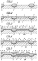
- an oxidation thermal treatment which may also be preceded by a deposition of silicon nitride according to a well known technique, is carried out to form an isolating dielectric layer 9, which in the area 8 at the far right side of the figures where it is shown the formation of a direct contact, is superimposed to the existent gate dielectric layer 4.
- the oxidation thermal treatment determines the diffusion of the dopant implanted in the EPM phase; diffusion that is symbolically highlighted in Fig. 5.
- the so-called MATRIX mask is formed which, as shown in the left side of the cross sections where it is shown the formation of the natural transistor (7), the MATRIX mask, as modified according to the invention, defines a central or channel area of the transistor.
- the interpoly dielectric layer 9 is etched and optionally a light implant LVS is performed in the channel zone of the transistors of the outer circuitry (not shown in the figures) as well as in the areas of direct contacts 8.
- LVS light implant
- the MATRIX mask shields the channel area of the natural transistor from the LVS implant.
- the channel area of the natural transistor is thus covered by the interpoly dielectric layer 9.
- a definition mask 12 of the polycrystalline silicon layer of second level is formed, as shown in Fig. 8. Over the channel area of the natural transistor this mask 12 has a width substantially smaller than the width of the MATRIX mask that practically defines the channel length of the transistor.
- the etching of the polysilicon through the mask 12 produces, as illustrated in the cross sections of Fig. 8, the definition of the gate structure of the natural transistor since the dielectric interpoly layer 9 acts as a mask of the selective etching of the polysilicon, for the underlying polysilicon of first level over the channel region of the natural transistor.
- Fig. 9 is a cross section that shows the structure after the removal of the POLY 2 mask 12 and the subsequent implant and diffusion of the source and drain regions of the integrated structures.
- the patterned layer 11 of polysilicon of second level in the area of the natural transistor is short circuited with the layer 5 of polysilicon of first level by direct superposition to the latter over the adjacent field oxide, for this reason the interpoly dielectric layer 9 that remains between poly 1 and poly 2 above the channel area of the natural transistor has not any influence.
- the invention allows for the realization of natural or low threshold transistors by exploiting the MATRIX mask, suitably modified, to define the channel length of natural transistors and thus eliminating the need for an additional masking step as required in the known processes for realizing also said low threshold transistors in addition to the normal enhancement-type transistors for the outer or ancillary circuitry of the memory array.
- the process of the invention can be performed according to the following characteristics and parameters: Implant Dose Energy Type Variation APT 1E12 100KeV B +/-0.5% EPM 6.5E12 120KeV B +/-0.5% LVS 1E12 45KeV B +/-0.5% S/D n+ 5E12 60KeV As +/- 1% S/D P+ 3E12 70KeV BF 2 +/- 1% Layer Thickness Variation Poly 1 1350 ⁇ +/- 225 ⁇ Poly 2 2000 ⁇ +/- 200 ⁇ SiW 2500 ⁇ +/- 250 ⁇ Ox interpoly 200 ⁇ +/- 20% Ox gate 190 ⁇ +/- 20%
Landscapes
- Engineering & Computer Science (AREA)
- Manufacturing & Machinery (AREA)
- Semiconductor Memories (AREA)
Claims (4)
- Procédé de fabrication d'un transistor naturel ou transistor à seuil bas (7) dans un circuit intégré comprenant également une matrice de cellules mémoire à grille flottante non volatiles comportant un double niveau de silicium polycristallin (5, 11), une couche diélectrique de grille (4) et une couche diélectrique interpoly (9) d'isolement entre les deux niveaux de silicium polycristallin, le procédé comprenant les étapes consistant à définir par un oxyde de champ (3) des zones actives, à former une couche d'oxyde de grille (4) sur les zones actives, à déposer et graver une couche de premier niveau (5) de silicium polycristallin dopé pour former les grilles flottantes (6) des cellules mémoires, à former ladite couche diélectrique (9) d'isolement interpoly sur les parties gravées de la couche de premier niveau de silicium polycristallin, à former un masque sur la zone de matrice mémoire, et en outre :former ledit masque dans des régions externes à la matrice mémoire pour définir la longueur de canal d'au moins un transistor naturel ou à seuil bas (7) à former en dehors de la zone de matrice mémoire ;graver sélectivement la couche diélectrique (9) d'isolement interpoly dans les zones non masquées par ledit masque ;enlever ledit masque et déposer une couche de second niveau (11) de silicium polycristallin dopé sur toute la structure ;graver au moyen d'un masque alloué (12) la couche de second niveau (11) de silicium polycristallin en gravant sélectivement le silicium polycristallin et en continuant à graver à travers la couche de premier niveau (8) de silicium polycristallin dans les zones actives du transistor naturel (7) en utilisant la couche diélectrique précédemment gravée (9) d'isolement interpoly comme masque, jusqu'à exposer la couche diélectrique de grille sous-jacente (4) ;graver sélectivement la couche diélectrique (9) d'isolement interpoly et la couche diélectrique de grille (4) en utilisant les couches de premier et second niveaux de silicium polycristallin comme masques ;d'où il résulte que, dans la région de canal du transistor naturel (7), la largeur du masque alloué (12) telle que mesurée dans la direction de la longueur de canal est inférieure à celle du masque définissant la longueur de canal, le masque alloué étant en outre conçu de sorte que la partie gravée de la couche de premier niveau de silicium polycristallin dans la zone du transistor naturel est recouverte à débordement et en contact avec la partie gravée de la couche de second niveau de silicium polycristallin sur l'oxyde de champ adjacent à la zone active du transistor.
- Procédé selon la revendication 1, comprenant en outre l'étape consistant à réaliser une implantation de décalage à basse tension dans les zones actives des transistors de type à enrichissement à former à l'extérieur de la zone de matrice en implantant à travers des ouvertures dans la couche diélectrique (9) et ledit masque sur la couche diélectrique (9) dans les zones actives des transistors de type à enrichissement.
- Procédé selon la revendication 1, comprenant en outre l'étape consistant à former des régions de caissons dans un substrat semi-conducteur.
- Procédé selon la revendication 1, dans lequel la couche diélectrique interpoly (9) est un multicouche oxydenitrure-oxyde.
Priority Applications (3)
| Application Number | Priority Date | Filing Date | Title |
|---|---|---|---|
| EP96830021A EP0785570B1 (fr) | 1996-01-22 | 1996-01-22 | Fabrication des transisors naturels dans un procédé de mémoire non-volatile |
| DE69625169T DE69625169D1 (de) | 1996-01-22 | 1996-01-22 | Herstellung von natürlichen Transistoren in einem Verfahren für nichtflüchtige Speicher |
| US08/784,967 US5923975A (en) | 1996-01-22 | 1997-01-16 | Fabrication of natural transistors in a nonvolatile memory process |
Applications Claiming Priority (1)
| Application Number | Priority Date | Filing Date | Title |
|---|---|---|---|
| EP96830021A EP0785570B1 (fr) | 1996-01-22 | 1996-01-22 | Fabrication des transisors naturels dans un procédé de mémoire non-volatile |
Publications (2)
| Publication Number | Publication Date |
|---|---|
| EP0785570A1 EP0785570A1 (fr) | 1997-07-23 |
| EP0785570B1 true EP0785570B1 (fr) | 2002-12-04 |
Family
ID=8225790
Family Applications (1)
| Application Number | Title | Priority Date | Filing Date |
|---|---|---|---|
| EP96830021A Expired - Lifetime EP0785570B1 (fr) | 1996-01-22 | 1996-01-22 | Fabrication des transisors naturels dans un procédé de mémoire non-volatile |
Country Status (3)
| Country | Link |
|---|---|
| US (1) | US5923975A (fr) |
| EP (1) | EP0785570B1 (fr) |
| DE (1) | DE69625169D1 (fr) |
Families Citing this family (9)
| Publication number | Priority date | Publication date | Assignee | Title |
|---|---|---|---|---|
| DE69732293D1 (de) * | 1997-08-27 | 2005-02-24 | St Microelectronics Srl | Herstellungsverfahren eines nativen MOS-P-Kanal-Transistors mit Verfahren für nichtflüchtige Speicher |
| US6162683A (en) * | 1997-12-19 | 2000-12-19 | Texas Instruments Incorporated | System and method for forming an inter-layer dielectric in floating gate memory devices |
| US6228782B1 (en) * | 1999-05-11 | 2001-05-08 | Advanced Micro Devices, Inc. | Core field isolation for a NAND flash memory |
| US6159802A (en) * | 1999-07-14 | 2000-12-12 | United Microelectronics Corp. | Method of forming a stack-gate of a non-volatile memory on a semiconductor wafer |
| US6806123B2 (en) | 2002-04-26 | 2004-10-19 | Micron Technology, Inc. | Methods of forming isolation regions associated with semiconductor constructions |
| US6756619B2 (en) * | 2002-08-26 | 2004-06-29 | Micron Technology, Inc. | Semiconductor constructions |
| US7244651B2 (en) * | 2003-05-21 | 2007-07-17 | Texas Instruments Incorporated | Fabrication of an OTP-EPROM having reduced leakage current |
| EP1492126A1 (fr) * | 2003-06-27 | 2004-12-29 | Dialog Semiconductor GmbH | Mémoire DRAM analogique ou à multi-niveau comprenant un transistor du typ naturel |
| US6958271B1 (en) * | 2003-08-04 | 2005-10-25 | Advanced Micro Devices, Inc. | Method of fabricating a dual-level stacked flash memory cell with a MOSFET storage transistor |
Family Cites Families (9)
| Publication number | Priority date | Publication date | Assignee | Title |
|---|---|---|---|---|
| DE3105925C2 (de) * | 1981-02-18 | 1983-01-05 | Westfaelische Metall Industrie Kg Hueck & Co, 4780 Lippstadt | Fahrzeugscheinwerfer, dessen Reflektor um zwei senkrecht zueinander verlaufende Achsen verstellbar ist |
| JPS5974677A (ja) * | 1982-10-22 | 1984-04-27 | Ricoh Co Ltd | 半導体装置及びその製造方法 |
| JP2509697B2 (ja) * | 1989-04-28 | 1996-06-26 | 株式会社東芝 | 半導体装置およびその製造方法 |
| KR930007527B1 (ko) * | 1990-09-22 | 1993-08-12 | 삼성전자 주식회사 | 스토리지 셀 어레이와 주변회로를 갖는 불휘발성 반도체 메모리 장치의 제조방법 및 그 구조 |
| KR960009995B1 (ko) * | 1992-07-31 | 1996-07-25 | 삼성전자 주식회사 | 반도체 장치의 제조 방법 및 그 구조 |
| US5412238A (en) * | 1992-09-08 | 1995-05-02 | National Semiconductor Corporation | Source-coupling, split-gate, virtual ground flash EEPROM array |
| US5554551A (en) * | 1994-11-23 | 1996-09-10 | United Microelectronics Corporation | Method of manufacture of an EEPROM cell with self-aligned thin dielectric area |
| KR0161402B1 (ko) * | 1995-03-22 | 1998-12-01 | 김광호 | 불휘발성 메모리 제조방법 |
| KR0144906B1 (ko) * | 1995-03-31 | 1998-07-01 | 김광호 | 불휘발성 메모리 소자 및 그 제조방법 |
-
1996
- 1996-01-22 DE DE69625169T patent/DE69625169D1/de not_active Expired - Lifetime
- 1996-01-22 EP EP96830021A patent/EP0785570B1/fr not_active Expired - Lifetime
-
1997
- 1997-01-16 US US08/784,967 patent/US5923975A/en not_active Expired - Lifetime
Also Published As
| Publication number | Publication date |
|---|---|
| EP0785570A1 (fr) | 1997-07-23 |
| US5923975A (en) | 1999-07-13 |
| DE69625169D1 (de) | 2003-01-16 |
Similar Documents
| Publication | Publication Date | Title |
|---|---|---|
| US5164806A (en) | Element isolating structure of semiconductor device suitable for high density integration | |
| US6514830B1 (en) | Method of manufacturing high voltage transistor with modified field implant mask | |
| JP4210347B2 (ja) | 高耐圧トランジスタ及びその製造方法 | |
| JP4846889B2 (ja) | 集積回路の製造方法 | |
| US4775642A (en) | Modified source/drain implants in a double-poly non-volatile memory process | |
| US6159795A (en) | Low voltage junction and high voltage junction optimization for flash memory | |
| US6211003B1 (en) | Semiconductor integrated circuit device and process for manufacturing the same | |
| US6027971A (en) | Methods of forming memory devices having protected gate electrodes | |
| US20030013309A1 (en) | Dual depth trench isolation | |
| US5329482A (en) | Semiconductor memory device and method for producing it | |
| US20020052073A1 (en) | Semiconductor device and manufacturing method thereof | |
| US6888191B2 (en) | Semiconductor device and fabrication process therefor | |
| KR100839053B1 (ko) | 다양한 기술 및 애플리케이션에 대해 쉽게 수정가능한주변 트랜지스터를 갖는 셀프-얼라인 콘택 비휘발성메모리에 대한 구조 및 프로세스 | |
| US5350706A (en) | CMOS memory cell array | |
| US20040137686A1 (en) | Method of forming an embedded memory including forming three silicon or polysilicon layers | |
| US5663080A (en) | Process for manufacturing MOS-type integrated circuits | |
| US6207991B1 (en) | Integrated non-volatile and CMOS memories having substantially the same thickness gates and methods of forming the same | |
| EP0785570B1 (fr) | Fabrication des transisors naturels dans un procédé de mémoire non-volatile | |
| JP2000133729A (ja) | 非サリサイド処理不揮発性メモリセル、非サリサイド処理高電圧トランジスタ、及びサリサイド処理接合低電圧トランジスタを含む電子デバイスの製法および電子デバイス | |
| US5872034A (en) | EPROM in double poly high density CMOS | |
| KR100387721B1 (ko) | 반도체소자의 제조방법 | |
| US6008093A (en) | Method of making a mask ROM | |
| EP0902466B1 (fr) | Procédé de fabrication d'un transistor MOS naturel à canal p avec un procédé pour mémoires non volatiles | |
| KR100295936B1 (ko) | 비휘발성반도체메모리장치및그제조방법 | |
| KR0138234B1 (ko) | 고전압 모오스 트랜지스터의 구조 |
Legal Events
| Date | Code | Title | Description |
|---|---|---|---|
| PUAI | Public reference made under article 153(3) epc to a published international application that has entered the european phase |
Free format text: ORIGINAL CODE: 0009012 |
|
| AK | Designated contracting states |
Kind code of ref document: A1 Designated state(s): DE FR GB IT |
|
| 17P | Request for examination filed |
Effective date: 19971121 |
|
| RAP3 | Party data changed (applicant data changed or rights of an application transferred) |
Owner name: STMICROELECTRONICS S.R.L. |
|
| 17Q | First examination report despatched |
Effective date: 20000919 |
|
| GRAG | Despatch of communication of intention to grant |
Free format text: ORIGINAL CODE: EPIDOS AGRA |
|
| GRAG | Despatch of communication of intention to grant |
Free format text: ORIGINAL CODE: EPIDOS AGRA |
|
| GRAH | Despatch of communication of intention to grant a patent |
Free format text: ORIGINAL CODE: EPIDOS IGRA |
|
| GRAH | Despatch of communication of intention to grant a patent |
Free format text: ORIGINAL CODE: EPIDOS IGRA |
|
| GRAA | (expected) grant |
Free format text: ORIGINAL CODE: 0009210 |
|
| AK | Designated contracting states |
Kind code of ref document: B1 Designated state(s): DE FR GB IT |
|
| REG | Reference to a national code |
Ref country code: GB Ref legal event code: FG4D |
|
| REF | Corresponds to: |
Ref document number: 69625169 Country of ref document: DE Date of ref document: 20030116 |
|
| PG25 | Lapsed in a contracting state [announced via postgrant information from national office to epo] |
Ref country code: DE Free format text: LAPSE BECAUSE OF FAILURE TO SUBMIT A TRANSLATION OF THE DESCRIPTION OR TO PAY THE FEE WITHIN THE PRESCRIBED TIME-LIMIT Effective date: 20030305 |
|
| ET | Fr: translation filed | ||
| PLBE | No opposition filed within time limit |
Free format text: ORIGINAL CODE: 0009261 |
|
| 26N | No opposition filed |
Effective date: 20030905 |
|
| PGFP | Annual fee paid to national office [announced via postgrant information from national office to epo] |
Ref country code: GB Payment date: 20051223 Year of fee payment: 11 |
|
| GBPC | Gb: european patent ceased through non-payment of renewal fee |
Effective date: 20070122 |
|
| PG25 | Lapsed in a contracting state [announced via postgrant information from national office to epo] |
Ref country code: GB Free format text: LAPSE BECAUSE OF NON-PAYMENT OF DUE FEES Effective date: 20070122 |
|
| PGFP | Annual fee paid to national office [announced via postgrant information from national office to epo] |
Ref country code: IT Payment date: 20080122 Year of fee payment: 13 |
|
| PGFP | Annual fee paid to national office [announced via postgrant information from national office to epo] |
Ref country code: FR Payment date: 20090128 Year of fee payment: 14 |
|
| REG | Reference to a national code |
Ref country code: FR Ref legal event code: ST Effective date: 20100930 |
|
| PG25 | Lapsed in a contracting state [announced via postgrant information from national office to epo] |
Ref country code: FR Free format text: LAPSE BECAUSE OF NON-PAYMENT OF DUE FEES Effective date: 20100201 |
|
| PG25 | Lapsed in a contracting state [announced via postgrant information from national office to epo] |
Ref country code: IT Free format text: LAPSE BECAUSE OF NON-PAYMENT OF DUE FEES Effective date: 20090122 |