EP0785603B1 - Dispositif laser à semiconducteur et méthode de fabrication - Google Patents
Dispositif laser à semiconducteur et méthode de fabrication Download PDFInfo
- Publication number
- EP0785603B1 EP0785603B1 EP97105580A EP97105580A EP0785603B1 EP 0785603 B1 EP0785603 B1 EP 0785603B1 EP 97105580 A EP97105580 A EP 97105580A EP 97105580 A EP97105580 A EP 97105580A EP 0785603 B1 EP0785603 B1 EP 0785603B1
- Authority
- EP
- European Patent Office
- Prior art keywords
- layer
- etching stop
- gaas
- stop layer
- double heterostructure
- Prior art date
- Legal status (The legal status is an assumption and is not a legal conclusion. Google has not performed a legal analysis and makes no representation as to the accuracy of the status listed.)
- Expired - Lifetime
Links
Images


Classifications
-
- H—ELECTRICITY
- H01—ELECTRIC ELEMENTS
- H01S—DEVICES USING THE PROCESS OF LIGHT AMPLIFICATION BY STIMULATED EMISSION OF RADIATION [LASER] TO AMPLIFY OR GENERATE LIGHT; DEVICES USING STIMULATED EMISSION OF ELECTROMAGNETIC RADIATION IN WAVE RANGES OTHER THAN OPTICAL
- H01S5/00—Semiconductor lasers
- H01S5/30—Structure or shape of the active region; Materials used for the active region
- H01S5/32—Structure or shape of the active region; Materials used for the active region comprising PN junctions, e.g. hetero- or double- heterostructures
- H01S5/323—Structure or shape of the active region; Materials used for the active region comprising PN junctions, e.g. hetero- or double- heterostructures in AIIIBV compounds, e.g. AlGaAs-laser, InP-based laser
- H01S5/32308—Structure or shape of the active region; Materials used for the active region comprising PN junctions, e.g. hetero- or double- heterostructures in AIIIBV compounds, e.g. AlGaAs-laser, InP-based laser emitting light at a wavelength less than 900 nm
- H01S5/32325—Structure or shape of the active region; Materials used for the active region comprising PN junctions, e.g. hetero- or double- heterostructures in AIIIBV compounds, e.g. AlGaAs-laser, InP-based laser emitting light at a wavelength less than 900 nm red laser based on InGaP
-
- H—ELECTRICITY
- H01—ELECTRIC ELEMENTS
- H01S—DEVICES USING THE PROCESS OF LIGHT AMPLIFICATION BY STIMULATED EMISSION OF RADIATION [LASER] TO AMPLIFY OR GENERATE LIGHT; DEVICES USING STIMULATED EMISSION OF ELECTROMAGNETIC RADIATION IN WAVE RANGES OTHER THAN OPTICAL
- H01S5/00—Semiconductor lasers
- H01S5/20—Structure or shape of the semiconductor body to guide the optical wave ; Confining structures perpendicular to the optical axis, e.g. index or gain guiding, stripe geometry, broad area lasers, gain tailoring, transverse or lateral reflectors, special cladding structures, MQW barrier reflection layers
- H01S5/22—Structure or shape of the semiconductor body to guide the optical wave ; Confining structures perpendicular to the optical axis, e.g. index or gain guiding, stripe geometry, broad area lasers, gain tailoring, transverse or lateral reflectors, special cladding structures, MQW barrier reflection layers having a ridge or stripe structure
- H01S5/223—Buried stripe structure
- H01S5/2231—Buried stripe structure with inner confining structure only between the active layer and the upper electrode
-
- H—ELECTRICITY
- H10—SEMICONDUCTOR DEVICES; ELECTRIC SOLID-STATE DEVICES NOT OTHERWISE PROVIDED FOR
- H10F—INORGANIC SEMICONDUCTOR DEVICES SENSITIVE TO INFRARED RADIATION, LIGHT, ELECTROMAGNETIC RADIATION OF SHORTER WAVELENGTH OR CORPUSCULAR RADIATION
- H10F30/00—Individual radiation-sensitive semiconductor devices in which radiation controls the flow of current through the devices, e.g. photodetectors
- H10F30/20—Individual radiation-sensitive semiconductor devices in which radiation controls the flow of current through the devices, e.g. photodetectors the devices having potential barriers, e.g. phototransistors
- H10F30/21—Individual radiation-sensitive semiconductor devices in which radiation controls the flow of current through the devices, e.g. photodetectors the devices having potential barriers, e.g. phototransistors the devices being sensitive to infrared, visible or ultraviolet radiation
- H10F30/22—Individual radiation-sensitive semiconductor devices in which radiation controls the flow of current through the devices, e.g. photodetectors the devices having potential barriers, e.g. phototransistors the devices being sensitive to infrared, visible or ultraviolet radiation the devices having only one potential barrier, e.g. photodiodes
- H10F30/223—Individual radiation-sensitive semiconductor devices in which radiation controls the flow of current through the devices, e.g. photodetectors the devices having potential barriers, e.g. phototransistors the devices being sensitive to infrared, visible or ultraviolet radiation the devices having only one potential barrier, e.g. photodiodes the potential barrier being a PIN barrier
-
- H—ELECTRICITY
- H10—SEMICONDUCTOR DEVICES; ELECTRIC SOLID-STATE DEVICES NOT OTHERWISE PROVIDED FOR
- H10F—INORGANIC SEMICONDUCTOR DEVICES SENSITIVE TO INFRARED RADIATION, LIGHT, ELECTROMAGNETIC RADIATION OF SHORTER WAVELENGTH OR CORPUSCULAR RADIATION
- H10F71/00—Manufacture or treatment of devices covered by this subclass
- H10F71/127—The active layers comprising only Group III-V materials, e.g. GaAs or InP
- H10F71/1272—The active layers comprising only Group III-V materials, e.g. GaAs or InP comprising at least three elements, e.g. GaAlAs or InGaAsP
-
- H—ELECTRICITY
- H10—SEMICONDUCTOR DEVICES; ELECTRIC SOLID-STATE DEVICES NOT OTHERWISE PROVIDED FOR
- H10H—INORGANIC LIGHT-EMITTING SEMICONDUCTOR DEVICES HAVING POTENTIAL BARRIERS
- H10H20/00—Individual inorganic light-emitting semiconductor devices having potential barriers, e.g. light-emitting diodes [LED]
- H10H20/01—Manufacture or treatment
- H10H20/011—Manufacture or treatment of bodies, e.g. forming semiconductor layers
- H10H20/013—Manufacture or treatment of bodies, e.g. forming semiconductor layers having light-emitting regions comprising only Group III-V materials
-
- H—ELECTRICITY
- H10—SEMICONDUCTOR DEVICES; ELECTRIC SOLID-STATE DEVICES NOT OTHERWISE PROVIDED FOR
- H10P—GENERIC PROCESSES OR APPARATUS FOR THE MANUFACTURE OR TREATMENT OF DEVICES COVERED BY CLASS H10
- H10P14/00—Formation of materials, e.g. in the shape of layers or pillars
- H10P14/20—Formation of materials, e.g. in the shape of layers or pillars of semiconductor materials
- H10P14/22—Formation of materials, e.g. in the shape of layers or pillars of semiconductor materials using physical deposition, e.g. vacuum deposition or sputtering
-
- H—ELECTRICITY
- H10—SEMICONDUCTOR DEVICES; ELECTRIC SOLID-STATE DEVICES NOT OTHERWISE PROVIDED FOR
- H10P—GENERIC PROCESSES OR APPARATUS FOR THE MANUFACTURE OR TREATMENT OF DEVICES COVERED BY CLASS H10
- H10P14/00—Formation of materials, e.g. in the shape of layers or pillars
- H10P14/20—Formation of materials, e.g. in the shape of layers or pillars of semiconductor materials
- H10P14/29—Formation of materials, e.g. in the shape of layers or pillars of semiconductor materials characterised by the substrates
- H10P14/2901—Materials
- H10P14/2907—Materials being Group IIIA-VA materials
- H10P14/2911—Arsenides
-
- H—ELECTRICITY
- H10—SEMICONDUCTOR DEVICES; ELECTRIC SOLID-STATE DEVICES NOT OTHERWISE PROVIDED FOR
- H10P—GENERIC PROCESSES OR APPARATUS FOR THE MANUFACTURE OR TREATMENT OF DEVICES COVERED BY CLASS H10
- H10P14/00—Formation of materials, e.g. in the shape of layers or pillars
- H10P14/20—Formation of materials, e.g. in the shape of layers or pillars of semiconductor materials
- H10P14/32—Formation of materials, e.g. in the shape of layers or pillars of semiconductor materials characterised by intermediate layers between substrates and deposited layers
- H10P14/3202—Materials thereof
- H10P14/3214—Materials thereof being Group IIIA-VA semiconductors
- H10P14/3218—Phosphides
-
- H—ELECTRICITY
- H10—SEMICONDUCTOR DEVICES; ELECTRIC SOLID-STATE DEVICES NOT OTHERWISE PROVIDED FOR
- H10P—GENERIC PROCESSES OR APPARATUS FOR THE MANUFACTURE OR TREATMENT OF DEVICES COVERED BY CLASS H10
- H10P14/00—Formation of materials, e.g. in the shape of layers or pillars
- H10P14/20—Formation of materials, e.g. in the shape of layers or pillars of semiconductor materials
- H10P14/32—Formation of materials, e.g. in the shape of layers or pillars of semiconductor materials characterised by intermediate layers between substrates and deposited layers
- H10P14/3202—Materials thereof
- H10P14/3214—Materials thereof being Group IIIA-VA semiconductors
- H10P14/3221—Arsenides
-
- H—ELECTRICITY
- H10—SEMICONDUCTOR DEVICES; ELECTRIC SOLID-STATE DEVICES NOT OTHERWISE PROVIDED FOR
- H10P—GENERIC PROCESSES OR APPARATUS FOR THE MANUFACTURE OR TREATMENT OF DEVICES COVERED BY CLASS H10
- H10P14/00—Formation of materials, e.g. in the shape of layers or pillars
- H10P14/20—Formation of materials, e.g. in the shape of layers or pillars of semiconductor materials
- H10P14/32—Formation of materials, e.g. in the shape of layers or pillars of semiconductor materials characterised by intermediate layers between substrates and deposited layers
- H10P14/3242—Structure
- H10P14/3244—Layer structure
- H10P14/3251—Layer structure consisting of three or more layers
-
- H—ELECTRICITY
- H10—SEMICONDUCTOR DEVICES; ELECTRIC SOLID-STATE DEVICES NOT OTHERWISE PROVIDED FOR
- H10P—GENERIC PROCESSES OR APPARATUS FOR THE MANUFACTURE OR TREATMENT OF DEVICES COVERED BY CLASS H10
- H10P14/00—Formation of materials, e.g. in the shape of layers or pillars
- H10P14/20—Formation of materials, e.g. in the shape of layers or pillars of semiconductor materials
- H10P14/34—Deposited materials, e.g. layers
- H10P14/3402—Deposited materials, e.g. layers characterised by the chemical composition
- H10P14/3414—Deposited materials, e.g. layers characterised by the chemical composition being group IIIA-VIA materials
- H10P14/3421—Arsenides
-
- H—ELECTRICITY
- H10—SEMICONDUCTOR DEVICES; ELECTRIC SOLID-STATE DEVICES NOT OTHERWISE PROVIDED FOR
- H10P—GENERIC PROCESSES OR APPARATUS FOR THE MANUFACTURE OR TREATMENT OF DEVICES COVERED BY CLASS H10
- H10P14/00—Formation of materials, e.g. in the shape of layers or pillars
- H10P14/20—Formation of materials, e.g. in the shape of layers or pillars of semiconductor materials
- H10P14/36—Formation of materials, e.g. in the shape of layers or pillars of semiconductor materials characterised by treatments done before the formation of the materials
-
- H—ELECTRICITY
- H01—ELECTRIC ELEMENTS
- H01S—DEVICES USING THE PROCESS OF LIGHT AMPLIFICATION BY STIMULATED EMISSION OF RADIATION [LASER] TO AMPLIFY OR GENERATE LIGHT; DEVICES USING STIMULATED EMISSION OF ELECTROMAGNETIC RADIATION IN WAVE RANGES OTHER THAN OPTICAL
- H01S2304/00—Special growth methods for semiconductor lasers
- H01S2304/02—MBE
-
- H—ELECTRICITY
- H01—ELECTRIC ELEMENTS
- H01S—DEVICES USING THE PROCESS OF LIGHT AMPLIFICATION BY STIMULATED EMISSION OF RADIATION [LASER] TO AMPLIFY OR GENERATE LIGHT; DEVICES USING STIMULATED EMISSION OF ELECTROMAGNETIC RADIATION IN WAVE RANGES OTHER THAN OPTICAL
- H01S5/00—Semiconductor lasers
- H01S5/04—Processes or apparatus for excitation, e.g. pumping, e.g. by electron beams
- H01S5/042—Electrical excitation ; Circuits therefor
- H01S5/0421—Electrical excitation ; Circuits therefor characterised by the semiconducting contacting layers
-
- H—ELECTRICITY
- H01—ELECTRIC ELEMENTS
- H01S—DEVICES USING THE PROCESS OF LIGHT AMPLIFICATION BY STIMULATED EMISSION OF RADIATION [LASER] TO AMPLIFY OR GENERATE LIGHT; DEVICES USING STIMULATED EMISSION OF ELECTROMAGNETIC RADIATION IN WAVE RANGES OTHER THAN OPTICAL
- H01S5/00—Semiconductor lasers
- H01S5/20—Structure or shape of the semiconductor body to guide the optical wave ; Confining structures perpendicular to the optical axis, e.g. index or gain guiding, stripe geometry, broad area lasers, gain tailoring, transverse or lateral reflectors, special cladding structures, MQW barrier reflection layers
- H01S5/2054—Methods of obtaining the confinement
- H01S5/2081—Methods of obtaining the confinement using special etching techniques
- H01S5/209—Methods of obtaining the confinement using special etching techniques special etch stop layers
-
- H—ELECTRICITY
- H01—ELECTRIC ELEMENTS
- H01S—DEVICES USING THE PROCESS OF LIGHT AMPLIFICATION BY STIMULATED EMISSION OF RADIATION [LASER] TO AMPLIFY OR GENERATE LIGHT; DEVICES USING STIMULATED EMISSION OF ELECTROMAGNETIC RADIATION IN WAVE RANGES OTHER THAN OPTICAL
- H01S5/00—Semiconductor lasers
- H01S5/30—Structure or shape of the active region; Materials used for the active region
- H01S5/32—Structure or shape of the active region; Materials used for the active region comprising PN junctions, e.g. hetero- or double- heterostructures
- H01S5/3211—Structure or shape of the active region; Materials used for the active region comprising PN junctions, e.g. hetero- or double- heterostructures characterised by special cladding layers, e.g. details on band-discontinuities
-
- Y—GENERAL TAGGING OF NEW TECHNOLOGICAL DEVELOPMENTS; GENERAL TAGGING OF CROSS-SECTIONAL TECHNOLOGIES SPANNING OVER SEVERAL SECTIONS OF THE IPC; TECHNICAL SUBJECTS COVERED BY FORMER USPC CROSS-REFERENCE ART COLLECTIONS [XRACs] AND DIGESTS
- Y02—TECHNOLOGIES OR APPLICATIONS FOR MITIGATION OR ADAPTATION AGAINST CLIMATE CHANGE
- Y02E—REDUCTION OF GREENHOUSE GAS [GHG] EMISSIONS, RELATED TO ENERGY GENERATION, TRANSMISSION OR DISTRIBUTION
- Y02E10/00—Energy generation through renewable energy sources
- Y02E10/50—Photovoltaic [PV] energy
- Y02E10/544—Solar cells from Group III-V materials
-
- Y—GENERAL TAGGING OF NEW TECHNOLOGICAL DEVELOPMENTS; GENERAL TAGGING OF CROSS-SECTIONAL TECHNOLOGIES SPANNING OVER SEVERAL SECTIONS OF THE IPC; TECHNICAL SUBJECTS COVERED BY FORMER USPC CROSS-REFERENCE ART COLLECTIONS [XRACs] AND DIGESTS
- Y02—TECHNOLOGIES OR APPLICATIONS FOR MITIGATION OR ADAPTATION AGAINST CLIMATE CHANGE
- Y02P—CLIMATE CHANGE MITIGATION TECHNOLOGIES IN THE PRODUCTION OR PROCESSING OF GOODS
- Y02P70/00—Climate change mitigation technologies in the production process for final industrial or consumer products
- Y02P70/50—Manufacturing or production processes characterised by the final manufactured product
-
- Y—GENERAL TAGGING OF NEW TECHNOLOGICAL DEVELOPMENTS; GENERAL TAGGING OF CROSS-SECTIONAL TECHNOLOGIES SPANNING OVER SEVERAL SECTIONS OF THE IPC; TECHNICAL SUBJECTS COVERED BY FORMER USPC CROSS-REFERENCE ART COLLECTIONS [XRACs] AND DIGESTS
- Y10—TECHNICAL SUBJECTS COVERED BY FORMER USPC
- Y10S—TECHNICAL SUBJECTS COVERED BY FORMER USPC CROSS-REFERENCE ART COLLECTIONS [XRACs] AND DIGESTS
- Y10S148/00—Metal treatment
- Y10S148/095—Laser devices
Definitions
- the present invention relates to a method for producing a compound semiconductor device such as the semiconductor laser device and a light emitting diode (LED). More particularly, the present invention relates to a semiconductor laser device having an excellent temperature property allowing continuous oscillation of visible light beams at room temperature, and to a method for producing a compound semiconductor device in which a semiconductor layer of a III-V group compound is formed on a GaAs substrate with high crystallinity.
- a compound semiconductor device such as the semiconductor laser device and a light emitting diode (LED). More particularly, the present invention relates to a semiconductor laser device having an excellent temperature property allowing continuous oscillation of visible light beams at room temperature, and to a method for producing a compound semiconductor device in which a semiconductor layer of a III-V group compound is formed on a GaAs substrate with high crystallinity.
- a semiconductor laser device capable of oscillating light beams in the range of short wavelengths.
- an (Al Y Ga 1-Y ) 0.5 In 0.5 P crystal (0 ⁇ Y ⁇ 1) which lattice-matches a GaAs substrate has called attention in industries as a material for a visible light beam semiconductor laser capable of radiating light beams having a wavelength of the 600 nm band.
- the (Al Y Ga 1-Y ) 0.5 In 0.5 P (0 ⁇ Y ⁇ 1) is hereinafter referred to as AlGaInP unless otherwise specified.
- MBE molecular beam epitaxy
- MOCVD metal organic chemical vapor deposition
- Figure 4 is a sectional view of a conventional AlGaInP group visible light semiconductor laser device produced by the MBE method.
- a first conductivity type GaAs buffer layer 72, a first conductivity type GaInP buffer layer 73, a first conductivity type AlGaInP clad layer 74, a GaInP active layer 75, a second conductivity type AlGaInP second clad layer 76 and a second conductivity type GaInP layer 90 are formed on a first conductivity type GaAs substrate 71 in such a manner that one layer is grown on another in this order by the MBE method.
- an insulation silicon nitride film 91 which has a 10 ⁇ m wide stripe groove extending to reach the second conductivity type GaInP layer 90.
- Electrodes 85 and 84 are formed on the insulation silicon nitride film 91 and on the back surface of the substrate 71, respectively.
- the semiconductor laser device shown in Figure 4 is a gain guided semiconductor laser device in which current is confined by the insulation silicon nitride film 91 having the stripe groove.
- This semiconductor laser device has an oscillation threshold level of 93 mA and can continuously oscillate visible light beams at room temperature.
- This type of the semiconductor laser device can not effectively diffuse heat generated in the active layer at the time of oscillation due to the low thermal conductivity of the AlGaInP crystal.
- the maximum temperature for continuous oscillation is as low as 35°C.
- a semiconductor laser device having not only a structure of effective heat emission but also a double hetero structure composed of AlGaInP crystal layers lattice-matched with a GaAs substrate will be produced if an AlGaAs crystal layer with comparatively high thermal conductivity and effective heat emission can be formed on the AlGaInP crystal layers by the MBE method.
- the AlGaAs crystal layer with high crystallinity may not be formed on the AlGaInP crystal layers lattice-matched with the GaAs substrate by the MBE method if the surface of the AlGaInP crystal layer is contaminated by impurities.
- the molecular beam radiation must be switched from P to As.
- the above contamination occurs at the time when the layer growth is temporarily stopped for this switching after the growth of the AlGaInP crystal layers is completed.
- impurities such as oxygen and steam in the atmosphere inside a MBE apparatus attach themselves to the surface of the crystal layer on which the growth is temporarily stopped.
- the temperature of the substrate must be raised to about 620°C or higher.
- In and P in the AlGaInP layers actively evaporate, causing to deteriorate the surface of the AlGaInP crystal layers. It is not possible to grow the AlGaAs crystal layer with high crystallinity on the deteriorated surface of the AlGaInP crystal layers.
- the semiconductor laser device having the AlGaInP crystal layers grown by the MBE method is normally of a gain-guided type as shown in Figure 4.
- the horizontal transverse mode of laser beams can not be fully controlled. Therefore, the development of an index-guided semiconductor laser device which can stabilize the horizontal transverse mode of laser beams is required also for the semiconductor laser device having AlGaInP crystals.
- Figure 5 is a sectional view of a conventional index-guided semiconductor laser device.
- a first conductivity type GaAs buffer layer 72, a first conductivity type AlGaInP first clad layer 74, a GaInP active layer 75, a second conductivity type AlGaInP second clad layer 76, a second conductivity type GaAs layer 78 and a second conductivity type InGaAs layer 100 are formed on a first conductivity type GaAs substrate 71 in such a manner that one layer is grown on another in this order by the MBE method.
- the GaInP active layer 75, the second conductivity type AlGaInP second clad layer 76, the second conductivity type GaAs layer 78 and the second conductivity type InGaAs layer 100 are etched to form a 10 ⁇ m wide ridge. This ridged surface is covered with a silicon oxide layer 101 except the top portion thereof. Electrodes 85 and 84 are then formed over the top ridged surface and on the back surface of the substrate 71, respectively.
- the semiconductor laser device of this structure is disadvantageous in that heat generated in the active layer 75 is not efficiently emitted outside the device due to the presence of recesses on the ridged surface formed by etching, as a result preventing continuous oscillation at room temperature.
- JP-A-63 104 493 on which the preamble of claim 1 is based, discloses a semiconductor laser device comprising an AlGaInP double hetero-structure disposed on a GaAs substrate.
- a GaAs layer is disposed over the double hetero-structure, and this layer is provided with a stripe groove that extends through the GaAs layer to reach the upper surface of the double hetero-structure.
- An AlGaAs layer is disposed over the GaAs layer so as to fill the stripe groove.
- a first aspect of the present invention provides a semiconductor laser device comprising: a GaAs substrate; a double heterostructure composed of (Al k Ga 1-k ) 0.5 In 0.5 P (0 ⁇ k ⁇ 1) crystals formed on the GaAs substrate; a GaAs optical absorption layer for absorbing light generated in the double heterostructure, formed over the double heterostructure and having a striped groove extending therethrough, and a regrowing Al y Ga 1-y As (0 ⁇ y ⁇ 1) layer formed on the GaAs optical absorption layer in such a manner so as to fill up the stripe groove, the regrowing Al y Ga 1-y As layer having a band gap energy greater than an optical energy generated within the double heterostructure so as to unify the horizontal transverse mode, characterised in that the laser device further comprises an (Al x Ga 1-x ) 0.5 In 0.5 P (0 ⁇ x ⁇ 1) etching stop layer formed between the double heterostructure and the optical absorption layer, the etching stop layer having a band
- a second (Al y Ga 1-y ) 0.5 In 0.5 P (0 ⁇ y ⁇ 1) etching stop layer is formed between the top surface of the GaAs optical absorption layer and the bottom surface of the regrowing Al y Ga 1-y As layer.
- a second aspect of the present invention provides a method of producing a semiconductor laser device comprising the steps of: forming a double heterostructure composed of (Al k Ga 1-k ) 0.5 In 0.5 P (0 ⁇ k ⁇ 1) crystals on a GaAs substrate, forming an (Al x Ga 1-x ) 0.5 In 0.5 P (0 ⁇ x ⁇ 1) etching stop layer on the double heterostructure, the etching stop layer having a band gap energy greater than an optical energy enerated within the double heterostructure; forming a GaAs optical absorption layer for absorbing light generated in the double heterostructure on the etching stop layer, forming a stripe groove extending through the GaAs optical absorption layer to reach the etching stop layer, radiating As molecular beams onto the layered substrate in a MBE apparatus while heating the layered substrate to exceed a temperature at which In and P in the etching stop layer evaporate so as to change the exposed portion at and near the upper surface of the etching stop layer
- a third aspect of the present invention provides a method of producing a semiconductor laser device comprising the steps of: forming a double heterostructure composed of (Al k Ga 1-k ) 0.5 In 0.5 P (0 ⁇ k ⁇ 1) crystals on a GaAs substrate, forming an (Al x Ga 1-x ) 0.5 In 0.5 P (0 ⁇ x ⁇ 1) first etching stop layer on the double heterostructure, the first etching stop layer having a band gap energy greater than an optical energy generated within the double heterostructure, forming a GaAs optical absorption layer for absorbing light generated in the double heterostructure on the (Al x Ga 1-x ) 0.5 In 0.5 P first etching stop layer, forming an (Al y Ga 1-y ) 0.5 In 0.5 P (0 ⁇ y ⁇ 1) second etching stop layer on the GaAs optical absorption layer, forming a stripe groove extending through the (Al y Ga 1-y ) 0.5 In 0.5 P second etching
- a fourth aspect of the present invention provides a method of producing a semiconductor laser device, the method comprising the steps of: forming a double heterostructure composed of (Al k Ga 1-k ) 0.5 In 0.5 P (0 ⁇ k ⁇ 1) crystals on a GaAs substrate, forming an (Al x Ga 1-x ) 0.5 In 0.5 P (0 ⁇ x ⁇ 1) etching stop layer on the double heterostructure, the etching stop layer having a band gap energy greater than an optical energy generated within the double heterostructure, forming a GaAs optical absorption layer for absorbing light generated in the double heterostructure on the etching stop layer, forming a stripe groove in the GaAs optical absorption layer having a depth not to reach the etching stop layer, radiating As molecular beams onto the multi-layered substrate in a MBE apparatus while heating the substrate to exceed a temperature at which the portion of the GaAs layer remaining evaporates so that the etching stop layer is exposed inside the stripe groove and the portion
- the method for producing the compound semiconductor device according to the present invention can provide a high quality compound semiconductor device having the Al X Ga 1-X As crystal layer of high crystallinity formed on the (Al Y Ga 1-Y ) 0.5 In 0.5 P crystal layer.
- the surface of the GaInP etching stop layer is purified in the MBE apparatus and the thermally stable GaAs layer is formed thereon before the AlGaAs layer is formed.
- the method of the present invention can present a visible light semiconductor laser device which can reduce optical absorption loss at the stripe groove and have a low threshold current.
- the semiconductor laser device includes the AlGaAs layer having relatively high thermal conductivity, which enables heat generated inside the double hetero structure comprising AlGaInP to be efficiently diffused outside the semiconductor laser device. Further, the semiconductor laser device of this invention, which is of the index-guided having the stripe groove inside, is provided with an excellent temperature property, allowing continuous oscillation of visible light beams of the unified horizontal transverse mode at room temperature.
- the GaInP etching stop layer does not include an active Al, which can prevent the layer from being easily contaminated.
- the invention described herein makes possible the objectives of (1) providing a method for producing a high quality compound semiconductor device in which an Al X Ga 1-X As crystal layer of high crystallinity is easily formed on a deteriorated surface of an (Al Y Ga 1-Y ) 0.5 In 0.5 P crystal layer, and (2) providing a semiconductor laser device having a structure of presenting excellent heat diffusion and capable of continuously oscillating visible light beams at room temperature.
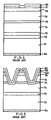
- Figure 1(d) is a sectional view of one example of the semiconductor laser device according to the present invention.
- the semiconductor laser device comprises a first conductivity type GaAs buffer layer 32, a first conductivity type GaInP buffer layer 33, a first conductivity type AlGaInP clad layer 34, a GaInP active layer 35, a second conductivity type AlGaInP clad layer 36, an (Al 0.7 Ga 0.3 ) 0.5 In 0.5 P first etching stop layer 37, a GaAs optical absorption layer 38 and an (Al 0.4 Ga 0.6 ) 0.5 In 0.5 P second etching stop layer 39 formed on a first conductivity type GaAs substrate 31 in this order.
- a stripe groove (5 ⁇ m width) is formed through the (Al 0.4 Ga 0.6 ) 0.5 In 0.5 P second etching stop layer 39 and the GaAs optical absorption layer 38 to reach the (Al 0.7 Ga 0.3 ) 0.5 In 0.5 P first etching stop layer 37.
- An Al 0.7 Ga 0.3 As layer 40 of a thickness of several molecules is formed on the surface of the first etching stop layer 37 exposed inside the stripe groove. Also, a Al 0.4 Ga 0.6 As layer 46 of a thickness of several molecules is formed on the surface of the second etching stop layer 39.
- a second conductivity type Al 0.7 Ga 0.3 As regrowing clad layer 41 is formed over the GaAs layer 38, the Al 0.7 Ga 0.3 As layer 40 and the Al 0.4 Ga 0.6 As layer 46 in such a manner that the stripe groove is filled up.
- the first conductivity type AlGaInP clad layer 34, the GaInP active layer 35 and the second conductivity type AlGaInP clad layer 36 constitute a double hetero structure, and therefore most light beams generated inside the active layer 35 are confined within this double hetero structure.
- the band gap energy in the GaAs layer 38 positioned on the both sides of the stripe groove is smaller than the energy of light beams generated in the active layer 35. Therefore, the GaAs layer 38 comparatively easily absorbs the light beams.
- the Al 0.7 Ga 0.3 As regrowing clad layer 41 is made to have a sufficiently large band gap and a sufficiently small refractive index required to confine the light beams generated in the active layer 35 within the double hetero structure. This results in producing an effective refractive index difference between the inside and the outside of the stripe groove formed above the double hetero structure, and thus the horizontal transverse mode of laser beams is unified.
- a second conductivity type GaAs cap layer 42 is formed on the second conductivity type Al 0.7 Ga 0.3 As regrowing clad layer 41, and electrodes 45 and 44 are formed on the surface of the second conductivity type GaAs cap layer 42 and on the back surface of the substrate 31, respectively.
- the first conductivity type GaAs buffer layer 32, the first conductivity type GaInP buffer layer 33, the first conductivity type AlGaInP clad layer 34, the GaInP active layer 35, the second conductivity type AlGaInP clad layer 36, the (Al 0.7 Ga 0.3 ) 0.5 In 0.5 P first etching stop layer 37, the GaAs optical absorption layer 38 and the (Al 0.4 Ga 0.6 ) 0.5 In 0.5 P second etching stop layer 39 are formed on the first conductivity type GaAs substrate 31 in such a manner that one layer is continuously grown on another in this order by the MBE method.
- the substrate temperature at this stage is in the range of about 480°C and about 570°C.
- the substrate 31 should not be moved outside the MBE apparatus to in order to keep the growing layers clean.
- the total thickness of the second conductivity type AlGaInP second clad layer 36 and the second conductivity type (Al 0.7 Ga 0.3 ) 0.5 In 0.5 P first etching stop layer 37 is as small as about 200 nm so that light beams generated in the active layer 35 can be transmitted to the GaAs optical absorption layer 38.
- the layered substrate is taken out of the MBE apparatus. Some portions of the (Al 0.4 Ga 0.6 ) 0.5 In 0.5 P second etching stop layer 39 and the GaAs optical absorption layer 38 are selectively etched using a photo mask 43 to form a stripe groove extending to reach the (Al 0.7 Ga 0.3 ) 0.5 In 0.5 P first etching stop layer 37 ( Figure 1(b)).
- impurities such as oxygen and steam in the atmosphere attach and contaminate the surface of the (Al 0.7 Ga 0.3 ) 0.5 In 0.5 P second conductivity type first etching stop layer 37.
- the contaminated surface of the layer 37 deteriorates the crystallinity of other layers to be grown thereon.
- the layered substrate is returned to the MBE apparatus where the layer 37 and the layer 39 are exposed to a sufficient amount of As molecular beams while the substrate temperature is raised to 620°C. The condition is maintained for several minutes.
- the Al 0.7 Ga 0.3 As layer 40 and the Al 0.4 Ga 0.6 As layer 46 formed in this step are thermally stable at a temperature below about 680°C, seldom causing evaporation of the composing elements. Thus, the evaporation of In and P from these layers 37 and 39 which is normally active at around 620°C can be avoided by being covered with these thin layers 40 and 46.
- the substrate temperature at radiation of As molecular beams is not limited to 620°C but can be about 580°C or higher at which In evaporates to form the Al 0.7 Ga 0.3 As layer 40 and the Al 0.4 Ga 0.6 As layer 46. P also evaporates in the temperature range where In evaporates. Therefore, both In and P are replaced with As under radiation of a sufficient amount of As molecular beams to form the layer 40 and the layer 46. At this time, in order to maintain the layer 40 and the layer 46 stable throughout the above stage, the substrate temperature is preferably about 680°C or lower.
- the second conductivity type Al 0.7 Ga 0.3 As regrowing clad layer 41 and the second conductivity type GaAs cap layer 42 are grown on the top surface of the layered substrate in such a manner that the stripe groove is filled up.
- the (Al 0.7 Ga 0.3 ) 0.5 In 0.5 P etching stop layer 37 and the (Al 0.4 Ga 0.6 ) 0.5 In 0.5 P etching stop layer 39 are significantly deteriorated caused by the evaporation of In and P therein at the temperature required to grow the second conductivity type regrowing clad layer 41.
- this deterioration can be avoided since these layers 37 and 39 are covered with the thermally stable Al 0.7 Ga 0.3 As layer 40 and Al 0.4 Ga 0.6 As layer 46, respectively.
- the Al 0.7 Ga 0.3 As regrowing clad layer 41 is formed to have a band gap energy greater than the energy of light beams generated in the active layer 35 by adjusting the Al content in the layer.
- the light beams generated in the active layer 35 can thus be confined within the double hetero structure.
- Electrodes 45 and 44 are formed on the top surface of the layered structure and on the back surface of the substrate 31, respectively, to produce the index guided semiconductor laser device as shown in Figure 1(d).
- the semiconductor laser device of this example comprising the double hetero structure including the AlGaInP crystal layers can continuously radiate light beams of a wavelength of 670 nm at room temperature.
- the index-guided semiconductor laser device having a stripe groove inside the device can radiate the laser beams of the unified horizontal transverse mode.
- the semiconductor laser device of this example is provided with the second conductivity type AlGaAs regrowing clad layer 41 including AlGaAs which has relatively high thermal conductivity, allowing heat generated in the active layer 35 to be efficiently diffused outside the semiconductor laser device.
- the semiconductor laser device of this example can show an excellent temperature property compared with the one shown in Figure 4.
- the (Al 0.7 Ga 0.3 ) 0.5 In 0.5 P layer 37 and the (Al 0.4 Ga 0.6 ) 0.5 In 0.5 P layer 39 were used as the etching stop layers.
- other composition ratio of AlGaInP than the above can also be used to form an AlGaInP etching stop layer which lattice-matches the substrate. This means that the lattice-matching with the substrate is possible for an etching stop layer formed of AlGaInP with an extensive variation of the composition ratio thereof, compared with, for example, AlGaAs.
- reduction of luminous efficiency caused by the failure in lattice-matching on the bottom portion of the stripe groove can be avoided, and laser beams of high optical output can be produced.
- the AlGaAs layer formed on the surface of the AlGaInP layer is not liable to be contaminated by impurities such as oxygen compared with, for example, an AlAs layer not including Ga.
- a semiconductor laser device was produced by the same method as described above but excluding the step of radiating As molecular beams and raising the substrate temperature to 620°C.
- the threshold current increased and therefore continuous oscillation at room temperature was not possible. This is because the surface of the second conductivity type AlGaInP first etching stop layer 37 was not purified and failed to grow a high quality AlGaAs regrowing clad layer 41 thereon.
- the Al 0.7 Ga 0.3 As layer 40 and the Al 0.4 Ga 0.6 As layer 46 being thin layers with a thickness of several molecules, do not give direct optical and electrical effects onto the properties of the semiconductor laser device.
- the semiconductor laser device of this example is provided with the(Al 0.4 Ga 0.6 ) 0.5 In 0.5 P layer as the second etching stop layer formed on the optical absorption layer 38.
- the crystallinity of the part of the AlGaAs regrowing layer 41 located above the optical absorption layer 38 then shows the same excellence as that of the part thereof grown above the stripe groove.
- the light beams generated in the active layer 35 are seldom transmitted into the part of the layer 41 located above the optical absorption layer 38, and therefore, a semiconductor laser device without the second etching stop layer 39 can obtain the same stable oscillation at room temperature as that of Example 1.
- Figure 1(d) is a sectional view of another example of the semiconductor laser device according to the present invention.
- the main differences between this example and Example 1 shown in Figure 1(d) are that in this example the (Al 0.4 Ga 0.6 ) 0.5 In 0.5 P layer is not formed on the optical absorption layer 38 and that an AlAs layer 49 is formed instead of the Al 0.7 Ga 0.3 As layer 40 of Example 1 on the etching stop layer in the bottom portion of the stripe groove.
- a first conductivity type GaAs buffer layer 32, a first conductivity type GaInP buffer layer 33, a first conductivity type AlGaInP first clad layer 34, a GaInP active layer 35, a second conductivity type AlGaInP second clad layer 36, an (Al 0.7 Ga 0.3 ) 0.5 In 0.5 P etching stop layer 37 and a GaAs optical absorption layer 38 are formed on a first conductivity type GaAs substrate 31 in such a manner that one layer is grown on another in this order by the MBE method.
- the total thickness of the second conductivity type AlGaInP second clad layer 36 and the second conductivity type (Al 0.7 Ga 0.3 ) 0.5 In 0.5 P etching stop layer 37 is as small as about 250 nm so that light beams generated in the active layer 35 can be transmitted to the GaAs optical absorption layer 38.
- GaAs optical absorption layer 38 is selectively etched using a photo mask 43 to form a stripe groove with the depth not to reach the (Al 0.7 Ga 0.3 ) 0.5 In 0.5 P etching stop layer 37 ( Figure 2(b)), leaving an about 100 nm thick GaAs layer between the bottom surface of the stripe groove and the top surface of the etching stop layer 37.
- the layered substrate is returned to the MBE apparatus where the layered substrate 31 covered with the GaAs layer is exposed to a sufficient amount of As molecular beams while the substrate temperature is raised to 720°C. The condition is maintained for several minutes.
- the GaAs remaining in the bottom portion of the stripe groove evaporates, and Ga, In and P present near the surface of the resultantly exposed (Al 0.7 Ga 0.3 ) 0.5 In 0.5 P etching stop layer 37 are replaced with As in the As molecular beams, changing the portions near the surface of the layer 37 to an AlAs layer 49 of a thickness of several molecules ( Figure 2(c)).
- This thin AlAs layer 49 is thermally stable at about 720°C, not causing significant evaporation of the composing elements. Thus, the evaporation of In and P from (Al 0.7 Ga 0.3 ) 0.5 In 0.5 P etching stop layer 37 which is normally active at around 720°C is avoided by being covered with this AlAs layer 49.
- the substrate temperature during the above step was 720°C, but in order to form the AlAs layer 49 it may be about 680°C or higher at which Ga and As evaporate. In and P also evaporate in the temperature range where Ga and As evaporate. Therefore, Ga, In and P present in the exposed portion of the (Al 0.7 Ga 0.3 ) 0.5 In 0.5 P layer 37 are replaced with As under radiation of a sufficient amount of As molecular beams to form the AlAs layer 49. At this time, in order to maintain the stability of the AlAs layer 49 throughout the above stage, the substrate temperature is preferably about 740°C or lower.
- the surface of the (Al 0.7 Ga 0.3 ) 0.5 In 0.5 P layer 37 is not exposed to the atmosphere, preventing it from being contaminated. Also, the surface of the GaAs layer contaminated by the exposition to the atmosphere can be purified by evaporating near the surface of the GaAs layer in the MBE apparatus.
- the AlAs layer 49 can prevent deterioration of the (Al 0.7 Ga 0.3 ) 0.5 In 0.5 P layer 37 caused by the evaporation of In and P which is normally active at a temperature about 580°C or higher.
- a second conductivity type Al 0.7 Ga 0.3 As regrowing clad layer 41 and a second conductivity type GaAs cap layer 42 are formed on the top surface of the layered substrate 31 in this order.
- the Al content in the Al 0.7 Ga 0.3 As regrowing clad layer 41 is determined so that the refractive index is low enough to confine the light beams generated in the active layer 35 within the same layer 35.
- Electrodes 45 and 44 are formed on the top face of the multi-layered structure and on the back surface of the substrate 31, respectively, to produce the index-guided semiconductor laser device as shown in Figure 2(d).
- Figure 3(d) is a sectional view of still another example of the semiconductor laser device according to the present invention.
- the semiconductor laser device comprises a first conductivity type GaAs buffer layer 52, a first conductivity type GaInP buffer layer 53, a first conductivity type AlGaInP first clad layer 54, a GaInP active layer 55, a second conductivity type AlGaInP second clad layer 56 (150 nm thickness), a GaInP first etching stop layer 57 (7 nm thickness), a GaAs optical absorption layer 58 and a GaInP second etching stop layer 59 formed on a first conductivity type GaAs substrate 51 in this order.
- the first conductivity type AlGaInP first clad layer 54, the GaInP active layer 55 and the second conductivity type AlGaInP second clad layer 56 constitute a double hetero structure.
- a stripe groove (5 ⁇ m width) is formed through the GaInP second etching stop layer 59 and the GaAs optical absorption layer 58 to reach the surface of the GaInP first etching stop layer 57.
- a second conductivity type Al 0.7 Ga 0.3 As regrowing clad layer 61 is formed over the layered structure in such a manner that the stripe groove is filled up.
- the Al content in the Al 0.7 Ga 0.3 As regrowing clad layer 61 is determined so that the refractive index is low enough (about 3.3) to confine the light beams generated in the active layer 55 within the double hetero structure.
- the thermal conductivity of this regrowing clad layer 61 is about 0.1 W/cm ⁇ deg.
- Electrodes 65 and 64 are formed on the top surface of the cap layer 62 and the back surface of the substrate 51, respectively.
- the first conductivity type GaAs buffer layer 52, the first conductivity type GaInP buffer layer 53, the first conductivity type AlGaInP first clad layer 54, the GaInP active layer 55, the second conductivity type AlGaInP second clad layer 56, the GaInP first etching stop layer 57, the GaAs optical absorption layer 58 and the GaInP second etching stop layer 59 are formed on the first conductivity type GaAs substrate 51 in such a manner that one layer is grown on another in this order.
- the substrate temperature at growing the layers is in the range of about 450°C and about 570°C.
- the substrate 51 should not be moved outside the MBE apparatus in order to keep the growing layers clean.
- the thickness of the second conductivity type AlGaInP second clad layer 56 is as small as about 150 nm so that light beams generated in the active layer 55 can be transmitted to the GaAs optical absorption layer 58.
- impurities such as oxygen and steam in the atmosphere attach the surface of the GaInP first etching stop layer 57.
- the GaInP layers 57 and 59 are exposed to a sufficient amount of As molecular beams so as to purify the surfaces thereof while the substrate temperature is raised to 620°C. The condition is maintained for several minutes.
- the GaAs layer 60 is thermally stable seldom causing evaporation of composing elements at a temperature below about 680°C.
- the substrate temperature at the stage of forming the GaAs layer 60 is not limited to 620°C but can be about 580°C or higher at which In evaporates to form the GaAs layer 60. P also evaporates in the temperature range where In evaporates. Therefore, both In and P are replaced with As under radiation of a sufficient amount of As molecular beams to form the GaAs layer 60. At this time, in order to maintain the stability of the GaAs layer 60 throughout the above stage, the substrate temperature is preferably about 680°C or lower.
- the GaAs layer 60 by forming the GaAs layer 60, the deterioration of the GaInP layers 57 and 59 caused by evaporation of In and P therein which is especially significant at a temperature of about 580°C or higher can be avoided at a temperature of about 680°C.
- a second conductivity type Al 0.7 Ga 0.3 As regrowing clad layer 61 and a second conductivity type GaAs cap layer 62 are grown on the top surface of the layered substrate in such a manner that the stripe groove is filled up.
- the GaAs layers 57 and 59 are significantly deteriorated caused by the evaporation of In and P therein at the temperature required to grow the Al 0.7 Ga 0.3 As regrowing clad layer 61. In this example, however, this deterioration can be avoided since these layers 57 and 59 are covered with the thermally stable GaAs layer 60.
- the Al 0.7 Ga 0.3 As regrowing clad layer 61 is formed to have a band gap energy (2.1 eV) greater than the energy of light beams (about 1.9 eV) generated in the active layer 55 by adjusting the Al content in the layer.
- the light beams generated in the active layer 55 can thus be confined within the double hetero structure.
- the band gap energy of the GaAs layer 58 having the stripe groove therethrough is smaller than the energy of light beams generated in the active layer 55, which light beams are therefore easily absorbed by the GaAs layer 58.
- an effective difference of the refractive indexes between the inside and the outside of the stripe groove located above the double hetero structure is produced, and thus the horizontal transverse mode of laser beams is unified.
- Electrodes 65 and 64 are formed on the top surface of the multi-layered structure and on the back surface of the substrate 51 to produce the index-guided semiconductor laser device as shown in Figure 3(d).
- the semiconductor laser device of this example can continuously radiate 670 nm wavelength light beams at room temperature, wherein the horizontal transverse mode of laser beams is unified.
- the GaAs layer 60 being a thin layer of a thickness of several molecules, does not directly give optical and electrical effects onto the properties of the semiconductor laser device.
- the semiconductor laser device of this example is provided with the second conductivity type AlGaAs regrowing clad layer 61 including AlGaAs which has relatively high thermal conductivity, allowing heat generated in the active layer 55 to be efficiently diffused outside the semiconductor laser device.
- the semiconductor laser device of this example can show an excellent temperature property compared with the one shown in Figure 4.
- a semiconductor laser device was produced by the same producing method described above but excluding the step of radiating As molecular beams and raising the substrate temperature to 620°C.
- the threshold current increased and continuous oscillation at room temperature was not possible. This is because the surface of the second conductivity type GaInP first etching stop layer 57 was not purified, failing in growing a high quality AlGaAs regrowing clad layer thereon.
- the semiconductor laser device of this example is provided with the GaInP layer as the second etching stop layer 59 formed on the GaAs layer 60.
- the crystallinity of the part of the AlGaAs regrowing layer 61 located above the optical absorption layer 58 then shows the same excellence as that of the part thereof grown above the stripe groove where the optical absorption layer 58 is removed.
- the light beams generated in the active layer 55 are seldom transmitted into the part of the layer 61 located above the optical absorption layer 58, and, therefore, a semiconductor laser device without the second etching stop layer 59 can obtain the same stable oscillation at room temperature as that of Example 7.
- the threshold current slightly increases. It is preferable therefore to also provide the GaInP second etching stop layer 59 on the optical absorption layer 58 so as to obtain a semiconductor laser device capable of stably oscillating at room temperature with the low threshold current.
- the GaInP first etching stop layer 57 of this example is 7 nm thick. It was found that a semiconductor laser device having the layer of a thickness of 20 nm failed to stably oscillate at room temperature. The reason is that when the thickness of the GaInP first etching stop layer 57 is large compared with the de Broglie wavelength, the optical absorption of the layer 57 increases, which increases the waveguide loss and therefore raises the threshold current.
- the thickness of the GaInP first etching stop layer 57 must be smaller than the electronic de Broglie wavelength. Practically, the thickness is preferably in the range of about 3 nm and about 15 nm.
- the band gap energy of the GaInP first etching stop layer 57 can be made greater than that of the active layer 55 by forming a quantum state in the layer 57, so as to reduce the optical absorption.
- the GaInP layer used as the etching stop layers which does not include the active Al has an advantage of being less contaminated by oxygen, steam and the like than the AlGaInP layer. Therefore, the semiconductor laser device of this example which has the GaInP etching stop layers disposed above the double hetero structure including AlGaInP layers is advantageous in being less contaminated during the producing process and also being capable of continuously oscillating visible light beams at room temperature.
- a layer made of GaAs was used as the optical absorption layer 58, but other materials which easily absorb the light beams generated in the active layer 55 such as AlGaAs may also be used.
- the double hetero structure are composed of the first conductivity type AlGaInP first clad layer, the GaInP active layer and the second conductivity type AlGaInP second clad layer.
- the structure may be formed of semiconductor layers of other compositions of the AlGaInP group: for example, layers formed of an AlInP three element mixed crystal as the first and the second clad layers, a layer formed of an AlGaInP four element mixed crystal as the active layer, or a layer having the quantum well structure or the superlattice structure can be used.
- An SCH structure can also be formed by providing between the clad layers and the active layer a guide which is small in gain and absorption loss.
Landscapes
- Physics & Mathematics (AREA)
- Condensed Matter Physics & Semiconductors (AREA)
- General Physics & Mathematics (AREA)
- Electromagnetism (AREA)
- Optics & Photonics (AREA)
- Geometry (AREA)
- Semiconductor Lasers (AREA)
- Physical Deposition Of Substances That Are Components Of Semiconductor Devices (AREA)
Claims (5)
- Dispositif laser à semi-conducteur comprenant :caractérisé en ce que le dispositif laser comprend, en outre, une couche d'arrêt d'attaque de (AlxGa1-x)0,5In0,5P (0≤x≤1) (37, 57) formée entre la double hétérostructure et la couche d'absorption optique (38, 58), la couche d'arrêt d'attaque (37, 57) ayant une énergie de bande interdite supérieure à une énergie optique générée au sein de la double hétérostructure, la rainure en bande s'étendant à travers la couche d'absorption optique (38, 58) jusqu'à la couche d'arrêt d'attaque, et la partie de ladite couche d'arrêt d'attaque (37, 57) située sous ladite rainure en bande, au niveau et à proximité de la surface supérieure de ladite couche d'arrêt d'attaque (37, 57), étant transformée en une couche de AlxGa1-xAs (0≤x≤1) (40, 49, 60) ayant une épaisseur de plusieurs molécules, préalablement à la recroissance de ladite couche de AlyGa1-yAs (0≤y≤1) (41, 61).un substrat de GaAs (31, 51);une double hétérostructure composée de cristaux de (AlkGa1-k)0,5In0,5P (0≤k≤1) formée sur le substrat de GaAs (31, 51);une couche d'absorption optique de GaAs (38, 58) destinée à absorber une lumière générée dans la double hétérostructure, qui est formée sur la double hétérostructure (37, 57) et à travers laquelle s'étend une rainure en bande; etune couche de AlyGa1-yAs (0≤y≤1) de recroissance (41, 61) formée sur la couche d'absorption optique de GaAs (38, 58) de manière à remplir complètement la rainure en bande, la couche de AlyGa1-yAs de recroissance (41, 61) ayant une énergie de bande interdite supérieure à une énergie optique générée au sein de la double hétérostructure, afin d'unifier le mode transversal horizontal;
- Dispositif laser à semi-conducteur tel que défini dans la revendication 1, dans lequel une seconde couche d'arrêt d'attaque de (AlyGa1-y)0,5In0,5P (0≤y≤1) (39, 59) est formée entre la surface supérieure de la couche d'absorption optique de GaAs (38, 58) et la surface inférieure de la couche de AlyGa1-yAs de recroissance (41, 61).
- Procédé pour produire un dispositif laser à semi-conducteur, comprenant les étapes qui consistent à:former une double hétérostructure composée de cristaux de (AlkGa1-k)0,5In0,5P (0≤k≤1) sur un substrat de GaAs (31, 51);former une couche d'arrêt d'attaque de (AlxGa1-x)0,5In0,5P (0≤x≤1) (37, 57) sur la double hétérostructure, la couche d'arrêt d'attaque (37, 57) ayant une énergie de bande interdite supérieure à une énergie optique générée au sein de la double hétérostructure;former une couche d'absorption optique de GaAs (38, 58) destinée à absorber une lumière générée dans la double hétérostructure, sur la couche d'arrêt d'attaque (37, 57);former une rainure en bande qui s'étend à travers la couche d'absorption optique de GaAs (38, 58) pour atteindre la couche d'arrêt d'attaque (37, 57);projeter des faisceaux moléculaires de As sur le substrat multicouche dans un appareil d'épitaxie par faisceaux moléculaires (MBE) tout en chauffant le substrat multicouche jusqu'à une température supérieure à une température à laquelle In et P de la couche d'arrêt d'attaque (37, 57) s'évaporent, afin de transformer la partie exposée au niveau et à proximité de la surface supérieure de la couche d'arrêt d'attaque dans la rainure en bande en une couche de AlxGa1-xAs (0≤x≤1) ayant une épaisseur de plusieurs molécules; etformer une couche de AlyGa1-yAs (0≤y≤1) (41, 49) sur la couche de AlxGa1-xAs (40, 60) et la couche d'absorption optique de GaAs (38, 58) de manière à remplir complètement la rainure en bande dans l'appareil de MBE, la couche de AlyGa1-yAs (41, 49) ayant une énergie de bande interdite supérieure à une énergie optique générée au sein de la double hétérostructure, afin d'unifier le mode transversal horizontal.
- Procédé pour produire un dispositif laser à semi-conducteur, comprenant les étapes qui consistent à:former une double hétérostructure composée de cristaux de (AlkGa1-k)0,5In0,5P (0≤k≤1) sur un substrat de GaAs (31, 51);former une première couche d'arrêt d'attaque de (AlxGa1-x)0,5In0,5P (0≤x≤1) (37, 57) sur la double hétérostructure, la première couche d'arrêt d'attaque (37, 57) ayant une énergie de bande interdite supérieure à une énergie optique générée au sein de la double hétérostructure;former une couche d'absorption optique de GaAs (38, 58) destinée à absorber une lumière générée dans la double hétérostructure, sur la première couche d'arrêt d'attaque de (AlxGa1-x)0,5In0,5P (37, 57);former une seconde couche d'arrêt d'attaque de (AlyGa1-y)0,5In0,5P (0≤y≤1) (39, 59) sur la couche d'absorption optique de GaAs (38, 58);former une rainure en bande qui s'étend à travers la seconde couche d'arrêt d'attaque de (AlyGa1-y)0,5In0,5P (39, 59) et la couche d'absorption optique de GaAs (38, 58) pour atteindre la première couche d'arrêt d'attaque de (AlxGa1-x)0,5In0,5P (37, 57);projeter des faisceaux moléculaires de As sur le substrat multicouche dans un appareil d'épitaxie par faisceaux moléculaires (MBE) tout en chauffant le substrat multicouche jusqu'à une température supérieure à une température à laquelle In et P des première et seconde couches d'arrêt d'attaque (37, 39, 57, 59) s'évaporent, afin de transformer respectivement les parties exposées au niveau et à proximité des surfaces supérieures des première et seconde couches d'arrêt d'attaque (37, 39, 57, 59) en une couche de AlxGa1-xAs (0≤x≤1) (40, 60) et une couche de AlyGa1-yAs (0≤y≤1) (46, 60) ayant une épaisseur de plusieurs molécules; etformer une couche de AlLGa1-LAs (0≤L≤1) (41, 61) sur la couche de AlxGa1-xAs (40, 60) et la couche de AlyGa1-yAs (46, 60) de manière à remplir complètement la rainure en bande dans l'appareil de MBE, la couche de AlLGa1-LAs (41, 61) ayant une énergie de bande interdite supérieure à une énergie optique générée au sein de la double hétérostructure, afin d'unifier le mode transversal horizontal.
- Procédé pour produire un dispositif laser à semi-conducteur, comprenant les étapes qui consistent à:former une double hétérostructure composée de cristaux de (AlkGa1-k)0,5In0,5P (0≤k≤1) sur un substrat de GaAs (31);former une couche d'arrêt d'attaque de (AlxGa1-x)0,5In0,5P (0≤x≤1) (37) sur la double hétérostructure, la couche d'arrêt d'attaque (37) ayant une énergie de bande interdite supérieure à une énergie optique générée au sein de la double hétérostructure;former une couche d'absorption optique de GaAs (38) destinée à absorber une lumière générée dans la double hétérostructure, sur la couche d'arrêt d'attaque (37);former dans la couche d'absorption optique de GaAs (38) une rainure en bande ayant une profondeur n'atteignant pas la couche d'arrêt d'attaque (37);projeter des faisceaux moléculaires de As sur le substrat multicouche dans un appareil d'épitaxie par faisceaux moléculaires (MBE) tout en chauffant le substrat jusqu'à une température supérieure à une température à laquelle la partie résiduelle de la couche de GaAs (38) s'évapore, afin que la couche d'arrêt d'attaque (37) soit exposée à l'intérieur de la rainure en bande et que la partie située au niveau et à proximité de la surface exposée de la couche d'arrêt d'attaque (37) soit transformée en une couche de AlAs ayant une épaisseur de plusieurs molécules; etformer une couche de AlyGa1-yAs (0≤y≤1) (41) sur la couche de AlAs et la couche d'absorption optique de GaAs (38) de manière à remplir complètement la rainure en bande dans l'appareil de MBE, la couche de AlyGa1-yAs (41) ayant une énergie de bande interdite supérieure à une énergie optique générée au sein de la double hétérostructure, afin d'unifier le mode transversal horizontal.
Applications Claiming Priority (11)
| Application Number | Priority Date | Filing Date | Title |
|---|---|---|---|
| JP120858/90 | 1990-05-09 | ||
| JP12085890 | 1990-05-09 | ||
| JP2120858A JP2537295B2 (ja) | 1990-05-09 | 1990-05-09 | 半導体レ―ザ素子及びその製造方法 |
| JP12991690 | 1990-05-18 | ||
| JP2129914A JPH0828326B2 (ja) | 1990-05-18 | 1990-05-18 | 化合物半導体層の製造方法 |
| JP2129916A JP2533962B2 (ja) | 1990-05-18 | 1990-05-18 | 半導体レ―ザ素子及びその製造方法 |
| JP129914/90 | 1990-05-18 | ||
| JP12991490 | 1990-05-18 | ||
| JP129916/90 | 1990-05-18 | ||
| EP91304161A EP0456485B1 (fr) | 1990-05-09 | 1991-05-09 | Méthode de production d'un composant à semi-conducteur |
| EP95115775A EP0695006B1 (fr) | 1990-05-09 | 1991-05-09 | Méthode de production d'un composé laser à semi-conducteur |
Related Parent Applications (3)
| Application Number | Title | Priority Date | Filing Date |
|---|---|---|---|
| EP95115775A Division EP0695006B1 (fr) | 1990-05-09 | 1991-05-09 | Méthode de production d'un composé laser à semi-conducteur |
| EP95115775.9 Division | 1991-05-09 | ||
| EP91304161.2 Division | 1991-05-09 |
Publications (3)
| Publication Number | Publication Date |
|---|---|
| EP0785603A2 EP0785603A2 (fr) | 1997-07-23 |
| EP0785603A3 EP0785603A3 (fr) | 1997-11-26 |
| EP0785603B1 true EP0785603B1 (fr) | 2003-04-02 |
Family
ID=27314128
Family Applications (3)
| Application Number | Title | Priority Date | Filing Date |
|---|---|---|---|
| EP91304161A Expired - Lifetime EP0456485B1 (fr) | 1990-05-09 | 1991-05-09 | Méthode de production d'un composant à semi-conducteur |
| EP95115775A Expired - Lifetime EP0695006B1 (fr) | 1990-05-09 | 1991-05-09 | Méthode de production d'un composé laser à semi-conducteur |
| EP97105580A Expired - Lifetime EP0785603B1 (fr) | 1990-05-09 | 1991-05-09 | Dispositif laser à semiconducteur et méthode de fabrication |
Family Applications Before (2)
| Application Number | Title | Priority Date | Filing Date |
|---|---|---|---|
| EP91304161A Expired - Lifetime EP0456485B1 (fr) | 1990-05-09 | 1991-05-09 | Méthode de production d'un composant à semi-conducteur |
| EP95115775A Expired - Lifetime EP0695006B1 (fr) | 1990-05-09 | 1991-05-09 | Méthode de production d'un composé laser à semi-conducteur |
Country Status (3)
| Country | Link |
|---|---|
| US (2) | US5255279A (fr) |
| EP (3) | EP0456485B1 (fr) |
| DE (3) | DE69129047T2 (fr) |
Families Citing this family (14)
| Publication number | Priority date | Publication date | Assignee | Title |
|---|---|---|---|---|
| JP2706369B2 (ja) * | 1990-11-26 | 1998-01-28 | シャープ株式会社 | 化合物半導体の成長方法及び半導体レーザの製造方法 |
| JP2708992B2 (ja) * | 1991-12-20 | 1998-02-04 | シャープ株式会社 | AlGaInP系半導体発光装置の製造方法 |
| JPH07162089A (ja) * | 1993-12-13 | 1995-06-23 | Mitsubishi Electric Corp | 可視光レーザダイオード及びその製造方法 |
| TW291585B (fr) * | 1994-07-04 | 1996-11-21 | Mitsubishi Chem Corp | |
| US5656539A (en) * | 1994-07-25 | 1997-08-12 | Mitsubishi Denki Kabushiki Kaisha | Method of fabricating a semiconductor laser |
| US5656829A (en) * | 1994-08-30 | 1997-08-12 | Showa Denko K.K. | Semiconductor light emitting diode |
| US5787104A (en) * | 1995-01-19 | 1998-07-28 | Matsushita Electric Industrial Co., Ltd. | Semiconductor light emitting element and method for fabricating the same |
| JP3373386B2 (ja) * | 1997-03-19 | 2003-02-04 | 富士通株式会社 | 半導体装置及びその製造方法 |
| US6888175B1 (en) | 1998-05-29 | 2005-05-03 | Massachusetts Institute Of Technology | Compound semiconductor structure with lattice and polarity matched heteroepitaxial layers |
| US6803603B1 (en) * | 1999-06-23 | 2004-10-12 | Kabushiki Kaisha Toshiba | Semiconductor light-emitting element |
| CN1324719C (zh) * | 2004-04-01 | 2007-07-04 | 光磊科技股份有限公司 | 一种发光二极管 |
| FR2876841B1 (fr) * | 2004-10-19 | 2007-04-13 | Commissariat Energie Atomique | Procede de realisation de multicouches sur un substrat |
| US8692286B2 (en) * | 2007-12-14 | 2014-04-08 | Philips Lumileds Lighing Company LLC | Light emitting device with bonded interface |
| CN102037575B (zh) * | 2008-03-27 | 2013-04-10 | 宋俊午 | 发光元件及其制造方法 |
Family Cites Families (15)
| Publication number | Priority date | Publication date | Assignee | Title |
|---|---|---|---|---|
| US4493142A (en) * | 1982-05-07 | 1985-01-15 | At&T Bell Laboratories | III-V Based semiconductor devices and a process for fabrication |
| JPS60192380A (ja) * | 1984-03-13 | 1985-09-30 | Mitsubishi Electric Corp | 半導体レ−ザ装置 |
| DE3683521D1 (de) * | 1985-04-02 | 1992-03-05 | Fujitsu Ltd | Thermisches aetzen eines verbindungshalbleiters. |
| JPH0728084B2 (ja) * | 1985-07-26 | 1995-03-29 | ソニー株式会社 | 半導体レーザー |
| JPS63104493A (ja) * | 1986-10-22 | 1988-05-09 | Nec Corp | 半導体レ−ザ素子 |
| US5068204A (en) * | 1987-03-27 | 1991-11-26 | Misawa Co. Ltd. | Method of manufacturing a light emitting element |
| JPS63284878A (ja) * | 1987-04-30 | 1988-11-22 | シーメンス、アクチエンゲゼルシヤフト | 埋込み活性層をもつレーザダイオードの製造方法 |
| JPS6437869A (en) * | 1987-08-03 | 1989-02-08 | Sanyo Electric Co | Solid-state image sensing device |
| JPS6437871A (en) * | 1987-08-04 | 1989-02-08 | Seiko Epson Corp | Solid-state image sensor |
| JPS6437870A (en) * | 1987-08-04 | 1989-02-08 | Seiko Epson Corp | Solid-state image sensing device and manufacture thereof |
| JPS6437873A (en) * | 1987-08-04 | 1989-02-08 | Hitachi Ltd | Semiconductor device and manufacture thereof |
| JPH01134985A (ja) * | 1987-11-19 | 1989-05-26 | Mitsubishi Electric Corp | 半導体レーザ装置 |
| JPH0828554B2 (ja) * | 1989-10-20 | 1996-03-21 | 三菱電機株式会社 | 半導体レーザ及びその製造方法 |
| US5058120A (en) * | 1990-02-28 | 1991-10-15 | Kabushiki Kaisha Toshiba | Visible light emitting semiconductor laser with inverse mesa-shaped groove section |
| JPH0513881A (ja) * | 1990-11-28 | 1993-01-22 | Matsushita Electric Ind Co Ltd | 半導体レーザの製造方法 |
-
1991
- 1991-05-09 EP EP91304161A patent/EP0456485B1/fr not_active Expired - Lifetime
- 1991-05-09 DE DE69129047T patent/DE69129047T2/de not_active Expired - Fee Related
- 1991-05-09 EP EP95115775A patent/EP0695006B1/fr not_active Expired - Lifetime
- 1991-05-09 DE DE69133230T patent/DE69133230T2/de not_active Expired - Fee Related
- 1991-05-09 DE DE69120865T patent/DE69120865T2/de not_active Expired - Fee Related
- 1991-05-09 US US07/698,001 patent/US5255279A/en not_active Expired - Lifetime
- 1991-05-09 EP EP97105580A patent/EP0785603B1/fr not_active Expired - Lifetime
-
1993
- 1993-06-21 US US08/080,004 patent/US5360762A/en not_active Expired - Lifetime
Also Published As
| Publication number | Publication date |
|---|---|
| EP0456485B1 (fr) | 1996-07-17 |
| US5360762A (en) | 1994-11-01 |
| EP0695006A1 (fr) | 1996-01-31 |
| DE69133230D1 (de) | 2003-05-08 |
| DE69129047D1 (de) | 1998-04-09 |
| EP0785603A2 (fr) | 1997-07-23 |
| DE69133230T2 (de) | 2003-12-11 |
| DE69120865D1 (de) | 1996-08-22 |
| EP0456485A2 (fr) | 1991-11-13 |
| EP0456485A3 (en) | 1992-04-15 |
| DE69129047T2 (de) | 1998-09-03 |
| EP0785603A3 (fr) | 1997-11-26 |
| EP0695006B1 (fr) | 1998-03-04 |
| DE69120865T2 (de) | 1997-01-23 |
| US5255279A (en) | 1993-10-19 |
Similar Documents
| Publication | Publication Date | Title |
|---|---|---|
| US6563851B1 (en) | Laser diode having an active layer containing N and operable in a 0.6 μm wavelength band | |
| EP0785603B1 (fr) | Dispositif laser à semiconducteur et méthode de fabrication | |
| JP3585817B2 (ja) | レーザダイオードおよびその製造方法 | |
| US7384479B2 (en) | Laser diode having an active layer containing N and operable in a 0.6 μm wavelength | |
| US5166945A (en) | Visible light surface emitting laser device | |
| US5270246A (en) | Manufacturing method of semiconductor multi-layer film and semiconductor laser | |
| US5588016A (en) | Semiconductor laser device | |
| US7176045B2 (en) | Laser diode operable in 1.3 μm or 1.5 μm wavelength band with improved efficiency | |
| EP0293000B1 (fr) | Dispositif émetteur de lumière | |
| US6884291B1 (en) | Laser diode having an active layer containing N and operable in a 0.6 μm wavelength band | |
| JP4078891B2 (ja) | 化合物半導体エピタキシャルウェハの製造方法および化合物半導体エピタキシャルウェハ | |
| EP0915542B1 (fr) | Laser à semiconducteur avec des couches de blocage du courant améliorées et méthode de fabrication | |
| CA2112319C (fr) | Laser a semiconducteur a gaine algainp | |
| JP2618677B2 (ja) | 半導体発光装置 | |
| JP2624881B2 (ja) | 半導体レーザ素子およびその製造方法 | |
| US5491709A (en) | Semiconductor laser device | |
| JP2909144B2 (ja) | 半導体レーザ装置及びその製造方法 | |
| Yoshikawa et al. | A novel technology for formation of a narrow active layer in buried heterostructure lasers by single-step MOCVD | |
| JP2502835B2 (ja) | 半導体レ―ザおよびその製造方法 | |
| JP2533962B2 (ja) | 半導体レ―ザ素子及びその製造方法 | |
| JP4192293B2 (ja) | AlGaAs系半導体レーザの製造方法、AlGaAs系半導体装置の製造方法および化合物半導体の成長方法 | |
| JP2664794B2 (ja) | 半導体レーザ素子の製造方法 | |
| JP2537295B2 (ja) | 半導体レ―ザ素子及びその製造方法 | |
| JP2839337B2 (ja) | 可視光半導体レーザ | |
| JPH0923039A (ja) | 半導体レーザの製造方法 |
Legal Events
| Date | Code | Title | Description |
|---|---|---|---|
| PUAI | Public reference made under article 153(3) epc to a published international application that has entered the european phase |
Free format text: ORIGINAL CODE: 0009012 |
|
| 17P | Request for examination filed |
Effective date: 19970423 |
|
| AC | Divisional application: reference to earlier application |
Ref document number: 695006 Country of ref document: EP |
|
| AK | Designated contracting states |
Kind code of ref document: A2 Designated state(s): DE FR GB |
|
| PUAL | Search report despatched |
Free format text: ORIGINAL CODE: 0009013 |
|
| AK | Designated contracting states |
Kind code of ref document: A3 Designated state(s): DE FR GB |
|
| 17Q | First examination report despatched |
Effective date: 20001012 |
|
| GRAH | Despatch of communication of intention to grant a patent |
Free format text: ORIGINAL CODE: EPIDOS IGRA |
|
| RIC1 | Information provided on ipc code assigned before grant |
Free format text: 7H 01S 5/32 A, 7H 01L 21/20 B, 7H 01L 33/00 B |
|
| GRAH | Despatch of communication of intention to grant a patent |
Free format text: ORIGINAL CODE: EPIDOS IGRA |
|
| GRAA | (expected) grant |
Free format text: ORIGINAL CODE: 0009210 |
|
| AC | Divisional application: reference to earlier application |
Ref document number: 0456485 Country of ref document: EP Kind code of ref document: P Ref document number: 0695006 Country of ref document: EP Kind code of ref document: P |
|
| AK | Designated contracting states |
Designated state(s): DE FR GB |
|
| REG | Reference to a national code |
Ref country code: GB Ref legal event code: FG4D |
|
| REF | Corresponds to: |
Ref document number: 69133230 Country of ref document: DE Date of ref document: 20030508 Kind code of ref document: P |
|
| ET | Fr: translation filed | ||
| PLBE | No opposition filed within time limit |
Free format text: ORIGINAL CODE: 0009261 |
|
| STAA | Information on the status of an ep patent application or granted ep patent |
Free format text: STATUS: NO OPPOSITION FILED WITHIN TIME LIMIT |
|
| 26N | No opposition filed |
Effective date: 20040105 |
|
| PGFP | Annual fee paid to national office [announced via postgrant information from national office to epo] |
Ref country code: GB Payment date: 20060503 Year of fee payment: 16 |
|
| PGFP | Annual fee paid to national office [announced via postgrant information from national office to epo] |
Ref country code: DE Payment date: 20060508 Year of fee payment: 16 |
|
| PGFP | Annual fee paid to national office [announced via postgrant information from national office to epo] |
Ref country code: FR Payment date: 20060515 Year of fee payment: 16 |
|
| GBPC | Gb: european patent ceased through non-payment of renewal fee |
Effective date: 20070509 |
|
| REG | Reference to a national code |
Ref country code: FR Ref legal event code: ST Effective date: 20080131 |
|
| PG25 | Lapsed in a contracting state [announced via postgrant information from national office to epo] |
Ref country code: DE Free format text: LAPSE BECAUSE OF NON-PAYMENT OF DUE FEES Effective date: 20071201 |
|
| PG25 | Lapsed in a contracting state [announced via postgrant information from national office to epo] |
Ref country code: GB Free format text: LAPSE BECAUSE OF NON-PAYMENT OF DUE FEES Effective date: 20070509 |
|
| PG25 | Lapsed in a contracting state [announced via postgrant information from national office to epo] |
Ref country code: FR Free format text: LAPSE BECAUSE OF NON-PAYMENT OF DUE FEES Effective date: 20070531 |