EP0785662A2 - Appareil de communication privée numérique pour interconnecter plusieurs éléments - Google Patents
Appareil de communication privée numérique pour interconnecter plusieurs éléments Download PDFInfo
- Publication number
- EP0785662A2 EP0785662A2 EP97440004A EP97440004A EP0785662A2 EP 0785662 A2 EP0785662 A2 EP 0785662A2 EP 97440004 A EP97440004 A EP 97440004A EP 97440004 A EP97440004 A EP 97440004A EP 0785662 A2 EP0785662 A2 EP 0785662A2
- Authority
- EP
- European Patent Office
- Prior art keywords
- interface
- bus
- module
- pcm
- modules
- Prior art date
- Legal status (The legal status is an assumption and is not a legal conclusion. Google has not performed a legal analysis and makes no representation as to the accuracy of the status listed.)
- Withdrawn
Links
- 238000004891 communication Methods 0.000 title claims abstract description 20
- 238000000034 method Methods 0.000 claims abstract description 9
- 230000002457 bidirectional effect Effects 0.000 claims description 3
- 230000011664 signaling Effects 0.000 description 19
- 102000006381 STAT1 Transcription Factor Human genes 0.000 description 6
- 108010044012 STAT1 Transcription Factor Proteins 0.000 description 6
- 102000004265 STAT2 Transcription Factor Human genes 0.000 description 5
- 108010081691 STAT2 Transcription Factor Proteins 0.000 description 5
- 238000007792 addition Methods 0.000 description 4
- 230000008859 change Effects 0.000 description 4
- 238000013475 authorization Methods 0.000 description 3
- 230000004044 response Effects 0.000 description 3
- 230000001360 synchronised effect Effects 0.000 description 3
- 101001066435 Homo sapiens Hepatocyte growth factor-like protein Proteins 0.000 description 2
- 101000880439 Homo sapiens Serine/threonine-protein kinase 3 Proteins 0.000 description 2
- 101000880431 Homo sapiens Serine/threonine-protein kinase 4 Proteins 0.000 description 2
- 102100037628 Serine/threonine-protein kinase 3 Human genes 0.000 description 2
- 102100037629 Serine/threonine-protein kinase 4 Human genes 0.000 description 2
- 230000000903 blocking effect Effects 0.000 description 2
- ZAIPMKNFIOOWCQ-UEKVPHQBSA-N cephalexin Chemical compound C1([C@@H](N)C(=O)N[C@H]2[C@@H]3N(C2=O)C(=C(CS3)C)C(O)=O)=CC=CC=C1 ZAIPMKNFIOOWCQ-UEKVPHQBSA-N 0.000 description 2
- 238000006243 chemical reaction Methods 0.000 description 2
- 238000010586 diagram Methods 0.000 description 2
- WFIZYGMIIMLKQI-UHFFFAOYSA-M ethyl-methyl-(4,6,11-trioxa-1-aza-5-silabicyclo[3.3.3]undecan-5-ylmethyl)sulfanium;iodide Chemical compound [I-].O1CCN2CCO[Si]1(C[S+](C)CC)OCC2 WFIZYGMIIMLKQI-UHFFFAOYSA-M 0.000 description 2
- 238000009434 installation Methods 0.000 description 2
- 230000002093 peripheral effect Effects 0.000 description 2
- 230000008569 process Effects 0.000 description 2
- 101000786631 Homo sapiens Protein SYS1 homolog Proteins 0.000 description 1
- 102100025575 Protein SYS1 homolog Human genes 0.000 description 1
- 230000002238 attenuated effect Effects 0.000 description 1
- 230000005540 biological transmission Effects 0.000 description 1
- 238000010276 construction Methods 0.000 description 1
- 230000008878 coupling Effects 0.000 description 1
- 238000010168 coupling process Methods 0.000 description 1
- 238000005859 coupling reaction Methods 0.000 description 1
- 230000001419 dependent effect Effects 0.000 description 1
- 238000013461 design Methods 0.000 description 1
- 238000000605 extraction Methods 0.000 description 1
- 238000003780 insertion Methods 0.000 description 1
- 230000037431 insertion Effects 0.000 description 1
- 230000000873 masking effect Effects 0.000 description 1
- 230000007246 mechanism Effects 0.000 description 1
- 230000009467 reduction Effects 0.000 description 1
- 238000012360 testing method Methods 0.000 description 1
Images


Classifications
-
- H—ELECTRICITY
- H04—ELECTRIC COMMUNICATION TECHNIQUE
- H04Q—SELECTING
- H04Q11/00—Selecting arrangements for multiplex systems
- H04Q11/04—Selecting arrangements for multiplex systems for time-division multiplexing
- H04Q11/0421—Circuit arrangements therefor
-
- H—ELECTRICITY
- H04—ELECTRIC COMMUNICATION TECHNIQUE
- H04M—TELEPHONIC COMMUNICATION
- H04M3/00—Automatic or semi-automatic exchanges
- H04M3/42—Systems providing special services or facilities to subscribers
- H04M3/56—Arrangements for connecting several subscribers to a common circuit, i.e. affording conference facilities
- H04M3/568—Arrangements for connecting several subscribers to a common circuit, i.e. affording conference facilities audio processing specific to telephonic conferencing, e.g. spatial distribution, mixing of participants
-
- H—ELECTRICITY
- H04—ELECTRIC COMMUNICATION TECHNIQUE
- H04M—TELEPHONIC COMMUNICATION
- H04M9/00—Arrangements for interconnection not involving centralised switching
- H04M9/02—Arrangements for interconnection not involving centralised switching involving a common line for all parties
- H04M9/022—Multiplex systems
- H04M9/025—Time division multiplex systems, e.g. loop systems
-
- H—ELECTRICITY
- H04—ELECTRIC COMMUNICATION TECHNIQUE
- H04M—TELEPHONIC COMMUNICATION
- H04M2201/00—Electronic components, circuits, software, systems or apparatus used in telephone systems
- H04M2201/22—Synchronisation circuits
-
- H—ELECTRICITY
- H04—ELECTRIC COMMUNICATION TECHNIQUE
- H04M—TELEPHONIC COMMUNICATION
- H04M3/00—Automatic or semi-automatic exchanges
- H04M3/42—Systems providing special services or facilities to subscribers
- H04M3/56—Arrangements for connecting several subscribers to a common circuit, i.e. affording conference facilities
- H04M3/561—Arrangements for connecting several subscribers to a common circuit, i.e. affording conference facilities by multiplexing
Definitions
- the present invention relates to a private digital communicarion apparatus for interconnecting a plurality of interface modules which communicate through a common bus.
- An object of the present invention is to give a further contribution to this field by providing further improvements in the performances of the apparatus mentioned above, in a particularly simple manner.
- Another object of the present invention is so to design an apparatus of the type mentioned above as to be compact, easy to realize and low cost.
- Each of the modules present on the bus may become the bus master manager. According to the situation of the connections present at a given instant and according to the rules established by the access manager (distributed among the various modules) it is decided who is the master module.
- Such apparatus is of multipoint type, uses a two-wire cable as a bus and the access to the bus is carried out through the time division (TDMA) technique.
- TDMA time division
- the various interface modules have a PCM connection to be able to be connected with the outside, i.e. it is possible to connect telephone sets, to establish connections to external public lines and to various services such as telefax, minitel, computers, printers, etc., and to whatever else has a PCM interface. In this way the modularity of the apparatus is maximum, different peripheral apparatuses can be connected to the same interface modules.
- a private digital communication apparatus has thus been obtained which is: able to connect quite a number of terminal apparatuses, extremely versatile, highly modular, of compact dimension, without a unique manager (and therefore a further apparatus) for the access to the bus.
- the communication system at issue is a multipoint one, it uses a two-wire cable as a bus and the access to the bus is carried out through the time division technique (TDMA).
- TDMA time division technique
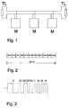
- the bus comprehensive of the line terminations TL is 200 m long at most, and the connections to the bus of each interface module M must not exceed 5 m.
- the maximum number of interface modules M that can be connected to the bus is 12. Different terminal elements can be connected to the interface modules M.
- eight telephone sets can be connected, of which two at the most, can be connected to external public lines, and four further interfaces at the most can be connected for various services such as telefax, minitel, computers, printers.
- the access to common bus control is carried out through the time division technique TDMA. From Fig.2 it can be seen that the frame structure is formed by one synchronization channel SYNC, one channel SIG for signalization and ten channels Ch1 to Ch10.
- Fig.2 shows the frame structure when transmitted by the master module.
- the master module will normally be a module which is synchronized by the external telephone network.
- the other modules should transmit in the channels while observing the bus propagation times.
- the propagation delay should be 1,4 us at most, for the modules located at the ends of the cable. In this case also the answer will be received after further 1,4 us. Therefore, it is necessary a delay of at least 2,8 us as guard time between the channels. A further 1 us has been added as a margin against eventual jitter and distortion problems and to easy the synchronization of the channels.
- the choice of the line code is not determined by the crosstalk signal-to-noise ratio or by the distortion of the cable attenuation, but rather by the intersymbol interference caused by the line reflections. These reflections are caused by the capacity of the connection cables of the interface modules and by the interfaces connected along the bus.
- the reflection worst case occurs when the bus has a higher impedance than the capacitive load of the connection cables of the modules.
- the distortion worst case, introduced by these reflections, occurs when the bus attenuation is low and the propagation time is long. In this case the reflections go back to the transmitter with a minimal attenuation.
- the line code has been chosen for minimizing the influence of these reflections; moreover, it must not have the DC component in order to facilitate and use the transformer coupling.
- This line code has no DC components and has a receive comparator independent of the received signal attenuation.
- each module must align the polarity of its transmitted and received symbols with the polarity of the alignment frame transmitted by the master module.
- the synchronization word SYNC is shown in detail in Fig.3.
- the first part of this time interval is without signal followed by a code violation V which is used by the receiver for recognizing the time reference located at the center of the violation itself. This time reference is used by the frame clock extraction mechanism.
- the code violation is inverted every frame to induce the introduced low-frequency jitter.
- the following four symbols S1 a S4 are used by the receive module to check that the correct synchronization has been reached. Moreover, they are used by the receiver in a slave manner to determine the polarity with which the transmitter shall transmit and receive on the bus. The polarity with which the slave module transmits and receives on the bus is referred to the polarity of the alignment frame received by the master module.
- the last four symbols I1 to I4 contain the address of the module authorized to use the signaling channel.
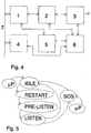
- the block diagram of the interface module is represented in Fig.4. It is formed by the following blocks:
- the line interface 1 is coupled with bus 7 through a transformer and establishes the connections between the various modules by using the channels preset as described previously.
- the PCM interface 3 handles the incoming and outgoing data and the related clocks. It also carries out the serial-to-parallel and parallel-to-serial conversions for the connections with the switching module 2. Such interface is able to handle both conventional telephone accesses, such as the analog ones, and the ISDN terminals.
- the master ISDN device will provide the clock from the ISDN connection when it will be active while it will provide the clock from a local free oscillator (PLL) when the ISDN connection will not be active.
- the clock thus provided, will be the synchronization clock of the bus 7.
- the ISDN terminal is slave when another ISDN terminal has an active ISDN connection.
- the local oscillator will generate a clock synchronized with the clock provided by the other active ISDN connection.
- the slave module becomes master (i.e. when its ISDN connection becomes active or when it is active and the master connection ends in) the clock generated by it will result very close in phase to the master one so as to assure that the change of the synchronization source does not penalize the other terminals and the communication in progress. To do so one must be sure that the interface modules dedicated to the ISDN terminals have their connections to bus 7 close enough so that the propagation delay towards the other terminals is quite the same.
- the first four channels of the PCM frame are used: the first two for the waiting signal and the local code, and the next two for the ISDN channel or two voice channels from analog network.
- the access control module 5 is responsible for the interpretation of the information of the line interface 1 relative to the connection status and it consequently reacts taking account also of the directives provided by microprocessor 6. It communicates with microprocessor 6 through interrupts and registers. Such module must be able to provide the apparatus with the following performances:
- the access control module 5 must also handle the signaling channel.
- the behaviour of the access Control module 5 can be summarized as follows also referring to the features listed above.
- a device which was not synchronism source and losses the synchronization is not allowed to become immediately synchronism source. As long as there is energy in the connection, it will try to synchronize itself again. Should the connection be interrupted (i.e. when there is no longer energy on the connection) it waits some instants and tries to become a synchronism source.
- a synchronism source that notes a disturbance in the synchronization frame will become active by sending the synchronization word, but it will not send data over the channel. It will remain active as long as the other peripheral units have recovered the synchronization losses (i.e. as long as the signaling channel is used as before) : in this circumstance the communications existing before the disturbance are recovered (if the microprocessor has not already erased the associated register). If, after a prefixed waiting time, the system has not recovered, the microprocessor will order the access control module to preset itself to an inactive state. At this point the interface module will not transmit any more and the frame structure will break off. Then the system starts again to operate as described previously.
- the microprocessor When a device is a synchronization source, the microprocessor makes sure that it recognizes the responses to the signaling requests from the other devices. If such responses do not arrive during a prefixed time interval, the microprocessor will again order the access control module to preset itself to an inactive state (considering that there is the probability that serious question exists, or that the device has not been installed). It will try again to become a synchronization source in response to an external event (handset hook-off, external telephone connection activated, other users' requests).
- an external event handset hook-off, external telephone connection activated, other users' requests.
- the restore starts with with one or more devices which transmit energy (each device transmits a different sequence) after a guard time and with a period of transmission followed by a silent period during which it recognizes that the other devices are transmitting.
- the guard and trasmission times are different for each interface module, depending on their identification number in the system.
- the signaling channel access is managed via software.
- the synchronism source module sends an authorization number with the synchronization word which communicates to the other modules who accesses the signaling channel.
- the manner in which the various modules are called in, is handled by the software.
- the access control module 5 hence handles only the processes of the tentatives of the various interface modules to become synchronization sources.
- the lock of the interface modules to the frame already present on the bus is handled by the line interface 1.
- the microprocessor forces the module into the inactive IDLE state; if there is no energy during a waiting time one passes into RESTART state. After the duration of the RESTART state, one passes into PRE-LISTEN state which is needed by the module to wait until the energy transmitted over the bus 7 becomes attenuated. Then one passes into the LISTEN state in which the module is in stand-by for some instants. If there is energy on the bus during this very short time, one passes again into the IDLE state otherwise one passes into the SOS state, i.e. synchronization source, to which one can access also via software; if there are remarkable disturbances one passes again into the IDLE state.
- SOS state i.e. synchronization source
- the access control module 5 is seen by microprocessor 6 as a series of registers and an interrupts source.
- the use of the frame resources over the bus 7 is defined by the occupancy of the different channels and by other predications on the status of the connection.
- the registers associated with the status of the bus are three read only registers of 8 bits BO-B7. TABLE 1 B7 B6 B5 B4 B3 B2 B1 B0 STAT1 SYN SIG CH1 CH2 CH3 CH4 CH5 CH6 STAT2 CH7 CH8 CH9 CH10 SYS NRG SYNCL OSS MST2 MST1 MST0
- registers STAT1 and STAT2 show which channels contain data (local energy recognition).
- Register SYS contains information about the bus management.
- Bit NRG shows if there is energy on the bus.
- SYNCLOSS indicates if the slave module is locked to the frame. When the module is synchronization source, it recognizes if there is a disturbance on the frame. To be noted that a 0 value, in this case, is not equivalent to a lack of disturbance. In this circumstance, it must be recognized at a higher level by recognizing a wrong value on transferred data.
- MST2-0 indicates the state of the access control module. Such states can be : inactive state, waiting or guard state and synchronization source state.
- Bit B7 of the register STAT1 cannot be masked since it does not generate interrupts. It gives information about the presence of energy in the time interval relative to the synchronism word. It is meaningless when SYNCLOSS is equal to 1, like also for any bit in the registers STAT1 and STAT2. This information should not be used except for switching an ISDN synchronism source.
- the microprocessor 6 drives the behaviour of the access control module of the priority of devices and of the synchronism sources through a command register T1.
- the microprocessor may force it into the IDLE state by setting B7 of T1 equal to 1, in the SOS state by setting B6 to 1, or may force it to try to become SOS (RESTART) by positioning 1 to bits B6 and B7. Moreover, it may force it to take an external synchronism to synchronize its PLL by setting B5 equal to 1.
- the other bits of register T1 are used for identifying the module and its priority.
- the signaling channel is handled with the help of a simple register and an interrupt.
- the interface module When the interface module is in the SOS state, it decides which module on the bus is allowed to access the signaling channel. This is done by the microprocessor through a programmable register.
- the content of this register is updated by the microprocessor 6 of the master module.
- the access control module 5 compares the signalling authorization number acquired by the line interface 1 and advises the microprocessor 6 when the signalling channel is proper, i.e. in the case where the number is in accord with its identification number.
- the arbitration for the priority of the synchronization is carried out by a mix of hardware and software.
- the line interface 1 handles the synchronization of the slave modules
- the access control module 5 handles the process of tentatives of the interface modules to become synchronization sources and the software handles the remainder.
- the different hardware-implemented guard times are made in such a way that the least number of terminals enter simultaneously into the RESTART state, and that only one of them becomes SOS.
- the numbering of modules provides unique values for these times.
- the time necessary for a slave module to become SOS, when the master drops or is removed from the system, is less than 32 milliseconds and depends on the smallest number given to one of the operating modules (the smaller this number, the shorter the time). If the programming has not changed in the meanwhile, the communications are automatically reactivated.
- the local processor decides when enabling the passage of the access control module 5 from the IDLE state to the RESTART state if all the automatic tentatives are unsuccessful.
- the state of the machine can be switched directly to the SOS state by the microprocessor 6. This function should never be used save for changing the SOS module at once (soft switching for ISDN sources).
- the state of the machine can also be directly switched into RESTART state by microprocessor 6. This function is used for easily doing a test of the system by creating a disturbance on the bus. It should never be used in the final software of use.
- the microprocessor 6 switches from the SOS state into the IDLE state when it senses the absence of energy in the signalling channel during a waiting time.
- the microprocessor 6 of the SOS module determines who accesses the signalling channel (through programming of the SIGC register).
- the switching module 2 is the hardware resource used for running from and toward the PCM interface 3 and the line interface 1.
- This module 2 shall store data from the PCM interface 3 into a buffer called PCM buffer.
- the buffer must be able to handle up to four different channels: one is preset for the insertion of a waiting music, another one is dedicated to local codec. The two remaining channels are dedicated to the interface with two telephone lines. For the sake of simplicity these four channels are fixed and are the first four channels of the PCM frame. Each channel has a dedicated register.
- TWIN buffer This buffer must be able to handle up to three different channels: one is dedicated to local codec, the two remaining channels are dedicated to the telephone lines.
- the microprocessor 6 accesses the register associated with the local codec for the hands-free functions.
- PCM interface 3 It must provide the PCM interface 3 with data from the TWIN buffer or by microprocessor 6, and obtain signalling from the line interface 1.
- the three registers of the TWIN buffer are multiplexed on the PCM interface 3.
- Each interface module carries out sums only over channels towards the local codec or towards the local line interfaces. This means that only three operations for frame are to be carried out. A sub-module containing the necessary expanders, adders and compressors is responsible for these operations.
- the PCM interface 3 has separable resources for the input and the output. Therefore, for a PCM channel, only one number is used for addressing a bidirectional channel: LOC for the local codec and PCx for the external telephone interface.
- the line interface 1 has shared resources for the input and the output. Therefore, two channels are necessary fort establishing a bidirectional channel (TWx e TWy). In the case of a conference three bus channels (TWx and TWy from two remote interface modules and TWxy from the local phone) are used.
- Fig. 6a-i there are represented the TWIN buffer 11 and the PCM buffer 14. Elements 12 and 13 are used for adding and switching the lines.
- Fig. 6a represents a simple communication between the local module and a module on the bus (two channels are used).
- Fig. 6b represents a simple communication between the local module and an external telephone line (no channels are used on the bus).
- Fig. 6c represents a simple communication between a module on the bus and an external telephone line (two channels are used).
- Fig. 6d represents a conference between the local module and two modules on the bus (three channels are used).
- Fig. 6e represents a conference between the local module, a module on the bus and an external telephone line (three channels are used).
- Fig. 6f represents a conference between an external telephone line and two modules on the bus (three channels are used).
- Fig. 6g represents a conference between the local module and two external telephone lines (no channels on the bus are used).
- Fig. 6h represents a conference between two external telephone lines and a module on the bus (three channels are used).
- the adder buffer is a destination for the channels on the bus similar to any TWIN buffer. All the channels pass through the adder. When the word to be passed shall not be summed, the input of the buffer is masked. When the word to be passed is a not stored operand, the operation is carried out at once when it arrives and the result is stored into a register of the TWIN buffer.
- the programming of the switching module 2 must give the following informations.
- the watch dog module 4 is so constructed that the software must access a low-speed dummy buffer so that the hardware is supposed not locked in a bad condition. Otherwise a counter, that takes the synchronism from the system, starts the reset of the microprocessor. The time requested for resetting the microprocessor is programmed through a 0 to 448 ms counter in steps of 32 ms.
- the microprocessor 6 handles the information to be able to drive the interface 3 and the modules 2,4 and 5.
- the invention has been implemented through a unique Application Specific Integrated Circuit (ASIC).
- ASIC Application Specific Integrated Circuit
Landscapes
- Engineering & Computer Science (AREA)
- Signal Processing (AREA)
- Multimedia (AREA)
- Computer Networks & Wireless Communication (AREA)
- Time-Division Multiplex Systems (AREA)
- Medicines Containing Antibodies Or Antigens For Use As Internal Diagnostic Agents (AREA)
- Cable Transmission Systems, Equalization Of Radio And Reduction Of Echo (AREA)
Applications Claiming Priority (2)
| Application Number | Priority Date | Filing Date | Title |
|---|---|---|---|
| ITMI960065 | 1996-01-17 | ||
| IT96MI000065A IT1281676B1 (it) | 1996-01-17 | 1996-01-17 | Apparato di comunicazione digitale di tipo privato per interconnettere una pluralita' di elementi |
Publications (2)
| Publication Number | Publication Date |
|---|---|
| EP0785662A2 true EP0785662A2 (fr) | 1997-07-23 |
| EP0785662A3 EP0785662A3 (fr) | 2003-07-02 |
Family
ID=11372922
Family Applications (1)
| Application Number | Title | Priority Date | Filing Date |
|---|---|---|---|
| EP97440004A Withdrawn EP0785662A3 (fr) | 1996-01-17 | 1997-01-17 | Appareil de communication privée numérique pour interconnecter plusieurs éléments |
Country Status (5)
| Country | Link |
|---|---|
| US (1) | US6275474B1 (fr) |
| EP (1) | EP0785662A3 (fr) |
| AU (1) | AU716969B2 (fr) |
| CA (1) | CA2195339A1 (fr) |
| IT (1) | IT1281676B1 (fr) |
Families Citing this family (2)
| Publication number | Priority date | Publication date | Assignee | Title |
|---|---|---|---|---|
| US7570724B1 (en) * | 1999-10-14 | 2009-08-04 | Pluris, Inc. | Method of link word synchronization |
| US20020012401A1 (en) * | 2000-05-23 | 2002-01-31 | Endevco Corporation | Transducer network bus |
Family Cites Families (11)
| Publication number | Priority date | Publication date | Assignee | Title |
|---|---|---|---|---|
| US3958084A (en) * | 1974-09-30 | 1976-05-18 | Rockwell International Corporation | Conferencing apparatus |
| DE2917675A1 (de) * | 1979-04-27 | 1980-11-06 | Hertz Inst Heinrich | Digitales zeitmultiplex-nachrichtensystem |
| US4289932A (en) * | 1979-10-15 | 1981-09-15 | Reed Roger R | Conferencing communications system |
| JPS59101943A (ja) * | 1982-12-03 | 1984-06-12 | Fuji Xerox Co Ltd | デイジタル信号伝送方式 |
| US4583089A (en) * | 1983-04-19 | 1986-04-15 | Foster Wheeler Energy Corporation | Distributed computer control system with variable monitor timers |
| US4739205A (en) * | 1986-02-24 | 1988-04-19 | Rockwell International Corporation | Telephone signal multiplexing system |
| US4797876A (en) * | 1987-07-10 | 1989-01-10 | Solid State Systems, Inc. | Conferencing bridge |
| US5425022A (en) * | 1989-06-16 | 1995-06-13 | British Telecommunications Public Limited Company | Data switching nodes |
| FR2648647B1 (fr) * | 1989-06-19 | 1991-08-23 | Alcatel Business Systems | Procede et dispositif d'arbitrage pour acces en emission au support de transmission d'un reseau de commutation reparti |
| US5359598A (en) * | 1990-06-22 | 1994-10-25 | Unisys Corporation | Voice server for digital communication network |
| US5963719A (en) * | 1996-01-22 | 1999-10-05 | Cabletron Systems, Inc. | Two-pin distributed ethernet bus architecture |
-
1996
- 1996-01-17 IT IT96MI000065A patent/IT1281676B1/it active IP Right Grant
-
1997
- 1997-01-14 AU AU10168/97A patent/AU716969B2/en not_active Ceased
- 1997-01-16 CA CA002195339A patent/CA2195339A1/fr not_active Abandoned
- 1997-01-17 EP EP97440004A patent/EP0785662A3/fr not_active Withdrawn
- 1997-01-17 US US08/779,289 patent/US6275474B1/en not_active Expired - Fee Related
Also Published As
| Publication number | Publication date |
|---|---|
| AU716969B2 (en) | 2000-03-09 |
| IT1281676B1 (it) | 1998-02-26 |
| US6275474B1 (en) | 2001-08-14 |
| EP0785662A3 (fr) | 2003-07-02 |
| ITMI960065A1 (it) | 1997-07-17 |
| CA2195339A1 (fr) | 1997-07-18 |
| AU1016897A (en) | 1997-07-24 |
| ITMI960065A0 (fr) | 1996-01-17 |
Similar Documents
| Publication | Publication Date | Title |
|---|---|---|
| KR950009577B1 (ko) | 전화 스테이션 세트와 사업용 통신 시스템을 상호 접속시키는 인터페이스 장치 및 통신 관리 장치 | |
| US6088362A (en) | Key telephone system without common control | |
| US4740955A (en) | Communications system having voice and digital data capability and employing a plurality of voice and data buses in main service unit and serial packetized transmission to and from telephones | |
| US4646289A (en) | Signal multiplexing circuit | |
| US5214650A (en) | Simultaneous voice and data system using the existing two-wire inter-face | |
| US5359598A (en) | Voice server for digital communication network | |
| CA2095508C (fr) | Bus de raccordement de systemes de commutation numeriques a protocoles incompatibles, systeme de repondeur telephonique et autocommutateur prive automatique a voix integree et enregistrement de texte a message | |
| US7529253B2 (en) | IP packet ready PBX expansion circuit for a conventional personal computer with expandable, distributed DSP architecture | |
| US3586782A (en) | Telecommunication loop system | |
| EP0135342B1 (fr) | Système de commutation | |
| AU6017394A (en) | Telecommunication switch with programmable communications services | |
| JP2697819B2 (ja) | 呼記録システム | |
| US4402073A (en) | Speech and data communication network | |
| US5014306A (en) | Voice and data telephone communication system and method | |
| US4394757A (en) | Frame format for PCM speech data in a telephone transmission system and digital telephone apparatus for use with this frame format | |
| US5333182A (en) | Arbitrary selecting of a terminal to be called in key telephone systems | |
| US5680589A (en) | Ring communication system using ISDN | |
| CA1311286C (fr) | Systeme telephonique numerique a clavier | |
| US4739205A (en) | Telephone signal multiplexing system | |
| US4602363A (en) | Expansion apparatus for use in communication systems | |
| AU716969B2 (en) | Private digital communication apparatus | |
| US5631955A (en) | Option bus | |
| US6751232B1 (en) | Method and apparatus for communicating data between first and second pairs of transceivers communicating on a common communications link | |
| EP0176953A2 (fr) | Système de communication simultanée de la parole et de données avec la possibilité de connexion aux réseaux publics ou privés | |
| Griffiths | ISDN network terminating equipment |
Legal Events
| Date | Code | Title | Description |
|---|---|---|---|
| PUAI | Public reference made under article 153(3) epc to a published international application that has entered the european phase |
Free format text: ORIGINAL CODE: 0009012 |
|
| AK | Designated contracting states |
Kind code of ref document: A2 Designated state(s): BE DE ES FR GB IT NL SE |
|
| RAP3 | Party data changed (applicant data changed or rights of an application transferred) |
Owner name: ALCATEL |
|
| RAP3 | Party data changed (applicant data changed or rights of an application transferred) |
Owner name: ALCATEL |
|
| PUAL | Search report despatched |
Free format text: ORIGINAL CODE: 0009013 |
|
| AK | Designated contracting states |
Designated state(s): BE DE ES FR GB IT NL SE |
|
| STAA | Information on the status of an ep patent application or granted ep patent |
Free format text: STATUS: THE APPLICATION IS DEEMED TO BE WITHDRAWN |
|
| 18D | Application deemed to be withdrawn |
Effective date: 20040103 |